3D Detector Simulation with Synopsys TCAD
|
|
|
- Grace Riley
- 5 years ago
- Views:
Transcription


1 Journée de la simulation 17/6/2013 3D Detector Simulation with Synopsys TCAD V. Gkougkousis1,2, A. Lounis 1,2, N. Dinu 1, A. Bassalat 1,3 1. Laboratoire de L'accélérateur Linéaire 2. Université Paris-SUD XI 3. CERN 1


2 Introduction Past advances and future intentions The tool: Status and capabilities Genic simulation principals General Process Flow Optimization strategies Implantation models Concrete cases Test Diode example 2D IBL single pixel simulation Full 3D IBL single and multiple pixel geometries Edgeless Detectors Status Dopant profile measurements Conclusions and plans Outline 2

 Radiated IBL structures simulation 1")


3 Passing to 3D Simulations Migrating from SILVACO TCAD to Synopsys Both process simulation and irradiation model integration IBL Voltage simulation (600V - 5 x10¹⁵neqcm-2) Radiated IBL structures simulation 1 Guard Ring Charge sharing and electrical field distributions Defects modeling and model testing Validate Edgeless VTT geometry and radiation hardness Guard Ring + Bias Rail Geometry and fabrication process flow simulation Detailed investigation of electrical field on detector edge Charge propagation in the substrate and boundary conditions effects Radiation hardness modeling and simulation No Guard Ring or Bias Rail Introduction & Status 3
 Multiple instances can be used, up to two per tool No multithreading support Portable Linux-based installation Out-of-the-box functionality No software dependences Memory and")
4 License One available license with minimum parallelization Three on-line license servers required Managed by LAL, accessible only via intranet No batch possibility at the moment (lxplus / ccage have no access to licenses) Multiple instances can be used, up to two per tool No multithreading support Portable Linux-based installation Out-of-the-box functionality No software dependences Memory and CPU consuming Central Licensing management plus bush capabilities essential Introduction & Status 4
 Introduce the required parameters (dose, energy, implantations) Set-up an appropriate meshing strategy for the desired")


5 Create a fabrication process flow to simulate geometry Associate with corresponding mask directly from GDS files (usually provided) Introduce the required parameters (dose, energy, implantations) Set-up an appropriate meshing strategy for the desired application Set up required re-meshing along the process to speed up simulation Introduce variables and create multiple experiments Preview strictures and profiles, feed-in parameters to other tools I. No need for detailed geometry definition II. Graphical interphase for speed with command functionality III. Comprehensive simulation I. Detailed process flow never known II. Re-meshing mandatory in each geometry change III. Optimized for small scale devices and interface simulation between different materials Generic Principals

6 1. The Mesh Define meshing strategy adapted to the specific geometry with finer cell size in transition regions Initial mesh valid until geometry change (first deposition, each), define remeshing strategy before Avoid thick photosensitive layers since they are even meshed after stripping Usually simulate fist few microns of substrate wafer and add full silicon thickness at the end In bilateral processes each flip causes geometry redefinition (no true bilateral integrated) 2. The model MC simulation or numerical solution to diffusion differential equations Number of particles to be simulated and extrapolate Physical model to be used Optimising
7 3. The refinements Implants energy and dose relative and absolute error Desired accuracy in concentration determination and profiles Grid refinements in transition regions (necessary to calculate solutions in dopants) Request multiprocessing 4. Implantation Model Analytic implantation: simple Gaussian/Pearson and dual Pearson functions, based on spatial distribution of ions described by moments depending on species, energy e.c.t. Numerical values given by tables Monte Carlo method atomistic simulation of ion implantation with Sentaurus MC, or Crystal-TRIM originated from the Transport of Ions in Matter (TRIM) code. Simulates ion implantation into single-crystalline materials or amorphous materials of arbitrary composition Optimizing.
 Dimensions 3000 x 3000 μm No Nitride layer p-spray Concrete Cases: Test")
8 Simple geometry Known dopant profiles Large structure Experimental iv curves to compere with simulation Pros: Simple geometry that allows model testing with simulated process flow No Backside structure Conns: Very large structure, enormous mesh with numerous cells which depletes available memory (in all platforms) Dimensions 3000 x 3000 μm No Nitride layer p-spray Concrete Cases: Test Diode 8


9 Complete pixel geometry Have to start from basic parameters (dopant profiles not exactly known) Small structure Experimental iv curves to compere with simulation Pros: Complicated geometry with multiple layers Backside processing present Have to do front and back side separately and merge results Small size so limited number of grid cells Conns: Aspects that are not yet completely understood in geometry file 24 hours for first imlantation Concrete Cases: IBL 2D Dimensions 250μm wafer thickness x80x25 Complete implantation 9


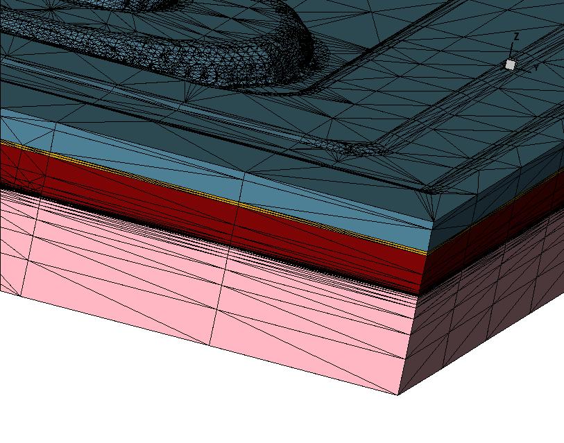
10 Adaptive meshing in transition regions Phosphorus profile Transition region between Si Oxide layer N profile in 2D IBL pixel simulation on the punch through side. Wafer is N with concentration of in the bulk. A thin 30nm Oxide layer remains. Concrete Cases: IBL 2D 10


11 Meshing of the photosensitive region Images of the same region of the pixel in the punch through side. Dimension ration distorted to display surface structures All 250 μm of the wafer are simulated Photoresist is present in the upper left plot Concrete Cases: IBL 2D 11


12 Complete 3D double sided pixel geometry Use basic parameters (dopant profiles not exactly known) Full depth substrate simulation Time of full single pixel run ~ 6h Bilateral process flow Concrete Cases: IBL 3D 12


13 Detail of the p-spray region between the pixels showing meshing, geometry and implants concentration Concrete Cases: IBL 3D 13

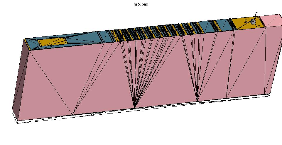
14 Concrete Cases: IBL 3D 14
15 Silicon Substrate Type: n, Phosphorus doped Orientation: 100 Resistivity 5000Ohm/cm 3 Thickness: 250μm (actual depth for simulation 5μm) Oxide Layer Photoresist n Implant Isotropic deposition of 150nm Anisotropic etching with a remaining 20nm layer 2μm isotropic deposition followed by strip etching after development Phosphorus at 60keV, dose of particles/cm 2 with angle of Default Parameters 15
16 P Spray Boron at 100keV, dose of particles/cm 2 with angle of Annealing 300 minutes at 900 C, pressure of 1atm (literature reference of 3 temperature zones and pressures in the order of 500torr) Metallization - Passivation Aluminum contacts formation from isotropic CVD deposit SiO 2 passivation layer for mechanical and electrical protection (no implication in simulation result) Default Parameters 16


17 Process Flow Complexity
18 GDS Files have been provided Not complete understuding of the fabrication process Scribe cleaning passivation poses simulation problem Several efforts are in the way Contacts in the near future with the industry (hoping to get input and details) Edgeless Detectors

19 Support a central licensing management which would allow multiple instances and parallelization Compare simulation results with experimental measurement in dopant profiles, charge shearing Simulate irradiated detectors and describe their behavior in the effort for radiation hardness Explore alternative geometries for bias rail / bias dot / guard ring structures Conclusions and plans
20 Backup


21 SIMS CNRS- Meudon (Cameca IMS 4F) Analytical technique to characterize the impurities in the surface and near surface (~30µm) region Relies on sputtering of a primary energetic ion beam ( kev) on sample surface and analysis of produced ionized secondary particles by mass spectrometry Good detection sensitivity for many elements: it can detect dopant densities as low as cm -3 Allows multielement detection, has a depth resolution of 1 to 5 nm and can give a lateral surface characterization on a scale of several microns Destructive method, since the act of the removing material by sputtering leaves a crater in a sample It determines the total dopant density profile Dopants profiles - SiMS 21


22 Analytical technique to characterize the majority carrier and active dopant concentration profiles in semiconductor structures 1. Pair of specially conditioned point contact probes which are stepped across the bevel surface of the semiconductor sample 2. Resistance between two probes is measured at each step 3. Resulting data computer processed into detailed carrier concentration and resistivity profiles from which dopant concentration profiles can be deduced Pros: Very high dynamic range ( Dopants profiles SRP cm-3) Capable of profiling very shallow junctions (nm regime) Conns: Destructive method 22


23 Dopants profiles n+/n p+/n N+ implant characteristics SIMS peak conc. Nn ~ 1x1019 cm-3 SRP peak conc. Nn ~ 8x1018 cm-3 P+ implant characteristics SIMS peak conc. Np ~ 3x1019 cm-3 SRP peak conc. Np ~ 5x1018 cm-3 Measurements on n-on n wafers Good overall SiMS SRP agreement 23 Not all implanted dopant atoms are integrated in lattice positions, not all electrically active LAL Pixel Group Activities 3/05/2013
CHAPTER 3 SIMULATION TOOLS AND
 CHAPTER 3 SIMULATION TOOLS AND Simulation tools used in this simulation project come mainly from Integrated Systems Engineering (ISE) and SYNOPSYS and are employed in different areas of study in the simulation
SILVACO International 0
 TCAD WORKSHOP USING SILVACO TCAD TOOLS Volume I This workshop will introduce you to process and device simulation using the Silvaco TCAD tools. It is assumed that you are familiar with basic concepts of
Taurus-Process. Multidimensional Process Simulation SYSTEMS PRODUCTS LOGICAL PRODUCTS PHYSICAL IMPLEMENTATION SIMULATION AND ANALYSIS LIBRARIES TCAD
 SYSTEMS PRODUCTS LOGICAL PRODUCTS PHYSICAL IMPLEMENTATION SIMULATION AND ANALYSIS LIBRARIES TCAD Aurora DFM WorkBench Davinci Medici Raphael Raphael-NES Silicon Early Access TSUPREM-4 Taurus-Device Taurus-Lithography
CMOS TECHNOLOGY- Chapter 2 in the Text
 CMOS TECHOLOGY- Chapter 2 in the Text CMOS Technology- Chapter 2 We will describe a modern CMOS process flow. In the simplest CMOS technologies, we need to realize simply MOS and MOS transistors for circuits
Victory Advanced Structure Editor. 3D Process Simulator for Large Structures
 Victory Advanced Structure Editor 3D Process Simulator for Large Structures Applications Victory Advanced Structure Editor is designed for engineers who need to create layout driven 3D process based structures
FACULTY OF ENGINEERING LAB SHEET. EOP3036 Fabrication and Packaging Technology TRIMESTER
 FACULTY OF ENGINEERING LAB SHEET EOP3036 Fabrication and Packaging Technology TRIMESTER 2 2017-2018 FP2 Simulation of fabrication processes and modelling of photodiodes Notes: 1. Maximum of TWO students
Integrated Simulation Solution for Advanced Power Devices
 Integrated Simulation Solution for Advanced Power Devices Objectives of this Presenation Presentation of simulation results for non-silicon power device types SiC Based Power Devices GaN Based Power Devices
Using TSUPREM-4 for Piezoresistor Design M. Hopcroft MAY2006 v1.01
 Using TSUPREM-4 for Piezoresistor Design M. Hopcroft MAY2006 v1.01 TSUPREM-4 can be used for predicting the characteristics of piezoresistors created by doping of silicon. However, some care must be taken
Optimization of thin n-in-p planar pixel modules for the ATLAS upgrade at HL-LHC arxiv: v1 [physics.ins-det] 12 Jan 2017
![Optimization of thin n-in-p planar pixel modules for the ATLAS upgrade at HL-LHC arxiv: v1 [physics.ins-det] 12 Jan 2017](/thumbs/73/68702264.jpg "Optimization of thin n-in-p planar pixel modules for the ATLAS upgrade at HL-LHC arxiv: v1 [physics.ins-det] 12 Jan 2017") Prepared for submission to JINST 8th International Workshop on Semiconductor Pixel Detectors for Particles and Imaging. 5-9 September 26 Sestri Levante Optimization of thin n-in-p planar pixel modules
Prepared for submission to JINST 8th International Workshop on Semiconductor Pixel Detectors for Particles and Imaging. 5-9 September 26 Sestri Levante Optimization of thin n-in-p planar pixel modules
FABRICATION OF CMOS INTEGRATED CIRCUITS. Dr. Mohammed M. Farag
 FABRICATION OF CMOS INTEGRATED CIRCUITS Dr. Mohammed M. Farag Outline Overview of CMOS Fabrication Processes The CMOS Fabrication Process Flow Design Rules EE 432 VLSI Modeling and Design 2 CMOS Fabrication
Thin n-in-p planar pixel modules for the ATLAS upgrade at HL-LHC
 Thin n-in-p planar pixel modules for the ATLAS upgrade at HL-LHC A. Macchiolo, J. Beyer, A. La Rosa, R. Nisius, N. Savic Max-Planck-Institut für Physik, Munich 8 th International Workshop on Semiconductor
Optimization of Photolithography Process Using Simulation
 Optimization of Photolithography Process Using Simulation Introduction The progress in semiconductor technology towards even smaller device geometries demands continuous refinements of photolithography
Post-Process Process CMOS Front End Engineering With Focused Ion Beams
 Post-Process Process CMOS Front End Engineering With Focused Ion Beams A. Lugstein 1, W. Brezna 1, B. Goebel 2, L. Palmetshofer 3, and E. Bertagnolli 1 1) Vienna University of Technology, Floragasse 7,
25 nm Omega FinFET: Three-dimensional Process and Device Simulations
 25 nm Omega FinFET: Three-dimensional Process and Device Simulations Abstract This Sentaurus simulation project provides a template setup for three-dimensional process simulation and device simulations
Three-dimensional Process Simulation for Advanced Silicon Semiconductor Devices
 Proceedings of the /11ternational Co11fere11ce 011 Advanced Semiconductor Devices and Microsystems October 20-24, 1996, Smole11ice, Slovakia 169 Three-dimensional Process Simulation for Advanced Silicon
Both equations are solved using a finite differences (iterative relaxation) method, which takes some time to converge.
 method, which takes some time to converge.") WEIGHTFIELD 2D Silicon Strip Detector Simulation V0.04 14 November 2011 markus.friedl@oeaw.ac.at Abstract WEIGHTFIELD is a program that allows simulating a silicon strip detector in two dimensions (crosssection).
WEIGHTFIELD 2D Silicon Strip Detector Simulation V0.04 14 November 2011 markus.friedl@oeaw.ac.at Abstract WEIGHTFIELD is a program that allows simulating a silicon strip detector in two dimensions (crosssection).
Victory Process. Full Physical 3D Semiconductor Simulator Etching and Deposition Simulation
 Victory Process Full Physical 3D Semiconductor Simulator Etching and Deposition Simulation Victory Process 3D Process Simulator Victory Process provides the capability to simulate comprehensive full process
Radiation hardness simulation of silicon thin detectors
 Radiation hardness simulation of silicon thin detectors F.Moscatelli 1,2, M. Petasecca 1, G.U. Pignatel 1 1 DIEI - Università, via G.Duranti,93 - Italy 2 IMM-CNR sez.di Bologna, via Gobetti 101 - Italy
Scanning Capacitance Microscopy Investigations of Focused Ion Beam Damage in Silicon
 Scanning Capacitance Microscopy Investigations of Focused Ion Beam Damage in Silicon W. Brezna, H. Wanzenböck, A. Lugstein, E. Bertagnolli, E. Gornik, J. Smoliner Institute for Solid State Electronics,
Luminous. Optoelectronic Device Simulator 4/15/05
 Optoelectronic Device Simulator 4/15/05 Contents Overview Key Benefits Applications Charge Coupled Devices (CCDs) Separate Absorption Multiplication (SAM) reach through avalanche photo detectors High speed
APPENDIX I OVERVIEW OF TCAD SIMULATION TOOL
 97 APPENDIX I OVERVIEW OF TCAD SIMULATION TOOL INTRODUCTION TCAD (Technology Computer Aided Design) is a technology that solves the equations representing the manufacturing process of Large Scale Integration
Taurus-Device. Multidimensional Device Simulation SYSTEMS PRODUCTS LOGICAL PRODUCTS PHYSICAL IMPLEMENTATION SIMULATION AND ANALYSIS LIBRARIES TCAD
 SYSTEMS PRODUCTS LOGICAL PRODUCTS PHYSICAL IMPLEMENTATION SIMULATION AND ANALYSIS LIBRARIES TCAD Aurora DFM WorkBench Davinci Medici Raphael Raphael-NES Silicon Early Access TSUPREM-4 Taurus-Device Taurus-Lithography
반도체공정 - 김원정. Lattice constant (Å)
") 반도체물리 - 반도체공정 - 김원정 Semiconductors Lattice constant (Å) 1 PN junction Transistor 2 Integrated circuit Integrated circuit originally referred to a miniaturized electronic circuit consisting of semiconductor
반도체물리 - 반도체공정 - 김원정 Semiconductors Lattice constant (Å) 1 PN junction Transistor 2 Integrated circuit Integrated circuit originally referred to a miniaturized electronic circuit consisting of semiconductor
Application Note. LDMOS Device and Process Simulation. Updated Crosslight Software Inc.
 Application Note LDMOS Device and Process Simulation Updated 2016.3 Crosslight Software Inc. Abstract--A technology template for the process and device simulation of a lateral double-diffused MOS (LDMOS)
Lighting up the Semiconductor World Semiconductor Device Engineering and Crosslight TCAD
 Lighting up the Semiconductor World Semiconductor Device Engineering and Crosslight TCAD What is TCAD? TCAD stands for Technology Computer Aided Design, it is a software tool for device engineers and professionals
Laser Applications for Photovoltaics Crystalline and Thin Film Technologies
 LASERS & MATERIAL PROCESSING I OPTICAL SYSTEMS I INDUSTRIAL METROLOGY I TRAFFIC SOLUTIONS I DEFENSE & CIVIL SYSTEMS Laser Applications for Photovoltaics Crystalline and Thin Film Technologies Back contact
Lecture 4a. CMOS Fabrication, Layout and Simulation. R. Saleh Dept. of ECE University of British Columbia
 Lecture 4a CMOS Fabrication, Layout and Simulation R. Saleh Dept. of ECE University of British Columbia res@ece.ubc.ca 1 Fabrication Fabrication is the process used to create devices and wires. Transistors
SAMPLE TUTORIAL. Introduction. Running Sample on UNIX systems. Barry Paul Linder, Spring 1996.
 SAMPLE TUTORIAL Barry Paul Linder, Spring 1996. Introduction SAMPLE is a simulation package that mimics a real processing laboratory. The machines SAMPLE simulates include an Exposure machine, a Developer
Integrated CMOS sensor technologies for the CLIC tracker
 Integrated CMOS sensor technologies for the CLIC tracker Magdalena Munker (CERN, University of Bonn) On behalf of the collaboration International Conference on Technology and Instrumentation in Particle
INTERNATIONAL TECHNOLOGY ROADMAP SEMICONDUCTORS 2001 EDITION MODELING AND SIMULATION FOR
 INTERNATIONAL TECHNOLOGY ROADMAP FOR SEMICONDUCTORS 2001 EDITION MODELING AND SIMULATION TABLE OF CONTENTS Scope...1 Difficult Challenges...1 Difficult Challenges 65 nm, Through 2007... 2 Difficult Challenges
LAB MANUAL. Silvaco ATLAS Device Simulation Software
 LAB MANUAL Silvaco ATLAS Device Simulation Software Centre for Detector & Related Software Technology (CDRST) Department of Physics & Astrophysics, University of Delhi 1 INDEX 1. OVERVIEW...3 2. ABOUT
Integrated Circuit Fabrication
 Integrated Circuit Fabrication Professor Dean Neikirk Department of Electrical and Computer Engineering The University of Texas at Austin world wide web: http://weewave.mer.utexas.edu Integrated circuits
A graphical user interface for multivariable analysis of silicon solar cells using scripted PC1D simulations
 Available online at www.sciencedirect.com ScienceDirect Energy Procedia 38 (2013 ) 72 79 SiliconPV: March 25-27, 2013, Hamelin, Germany A graphical user interface for multivariable analysis of silicon
Bulk MEMS Layout 2017 Dr. Lynn Fuller, Casey Gonta, Patsy Cadareanu Webpage:
 ROCHESTER INSTITUTE OF TECHNOLOGY MICROELECTRONIC ENGINEERING Bulk MEMS Layout 2017 Dr. Lynn Fuller, Casey Gonta, Patsy Cadareanu Webpage: http://people.rit.edu/lffeee 82 Lomb Memorial Drive Rochester,
(12) Patent Application Publication (10) Pub. No.: US 2013/ A1
 Patent Application Publication (10) Pub. No.: US 2013/ A1") US 2013 0082320A1 (19) United States (12) Patent Application Publication (10) Pub. No.: US 2013/0082320 A1 Alberhasky et al. (43) Pub. Date: Apr. 4, 2013 (54) STRAPPED DUAL-GATE VDMOS DEVICE (52) U.S.
US 2013 0082320A1 (19) United States (12) Patent Application Publication (10) Pub. No.: US 2013/0082320 A1 Alberhasky et al. (43) Pub. Date: Apr. 4, 2013 (54) STRAPPED DUAL-GATE VDMOS DEVICE (52) U.S.
ESD Protection Device Simulation and Design
 ESD Protection Device Simulation and Design Introduction Electrostatic Discharge (ESD) is one of the major reliability issues in Integrated Circuits today ESD is a high current (1A) short duration (1ns
Status of PEMC Steve Arthur 8/18/2016
 Status of PEMC Steve Arthur 8/18/2016 CNSE : Joe Piccirillo, PY Hung, Sean Valente, Tom Gorczyca GE : Ron Olson, Mike Hartig, Yang Sui, Andy Minnick, Matt Edmonds, Tim VandenBriel, Kevin Shatley, Justin
A New Model for Optical Crosstalk in SinglePhoton Avalanche Diodes Arrays
 A New Model for Optical Crosstalk in SinglePhoton Avalanche Diodes Arrays I. Rech, A. Ingargiola, R. Spinelli, S. Marangoni, I. Labanca, M. Ghioni, S. Cova Dipartimento di Elettronica ed Informazione Politecnico
Reflectivity Calculation Program
 Reflectivity Calculation Program This optional program allows calculation of the reflectivity spectrum at any incidence angle from the wavelength distribution of the sample n and k values. Additionally,
Guide to Using TCAD with Examples
 Guide to Using TCAD with Examples Silvaco 4701 Patrick Henry Drive, Bldg. 6 Santa Clara, CA 95054 Telephone (408) 567-1000 Internet: www.silvaco.com February 4, 2009 SILVACO Page 1 Guide to Using TCAD
Programming Characteristics on Three-Dimensional NAND Flash Structure Using Edge Fringing Field Effect
 JOURNAL OF SEMICONDUCTOR TECHNOLOGY AND SCIENCE, VOL.14, NO.5, OCTOBER, 2014 http://dx.doi.org/10.5573/jsts.2014.14.5.537 Programming Characteristics on Three-Dimensional NAND Flash Structure Using Edge
Modeling of Surface Reflectance of Acid Textured Multicrystalline Silicon Wafer for Solar Cell Application
 International Journal of Electronics and Computer Science Engineering 1065 Available Online at www.ijecse.org ISSN- 2277-1956 Modeling of Surface Reflectance of Acid Textured Multicrystalline Silicon Wafer
Flash memory cells data loss caused by total ionizing dose and heavy ions
 Cent. Eur. J. Phys. 12(10) 2014 725-729 DOI: 10.2478/s11534-014-0503-6 Central European Journal of Physics Flash memory cells data loss caused by total ionizing dose and heavy ions Research Article Andrey
Level set modeling of the orientation dependence of solid phase epitaxial regrowth
 Level set modeling of the orientation dependence of solid phase epitaxial regrowth Saurabh Morarka a Department of Electrical and Computer Engineering, University of Florida, Gainesville, Florida 32611-6200
Endcap Modules for the ATLAS SemiConductor Tracker
 Endcap Modules for the ATLAS SemiConductor Tracker RD3, Firenze, September 29 th, 23 Richard Nisius (MPI Munich) nisius@mppmu.mpg.de (For the ATLAS-SCT Collaboration) The plan of this presentation Introduction
Application of MCNP Code in Shielding Design for Radioactive Sources
 Application of MCNP Code in Shielding Design for Radioactive Sources Ibrahim A. Alrammah Abstract This paper presents three tasks: Task 1 explores: the detected number of as a function of polythene moderator
VEECO FPP Point Probe Operating Manual
 VEECO FPP-5000 4-Point Probe Operating Manual Version: 1.0 May 2013 UNIVERSITY OF TEXAS AT ARLINGTON Nanofabrication Research and Teaching Facility TABLE OF CONTENTS 1. Introduction....2 1.1 Scope of Work....2
republished with permission from Casa Software Ltd. Figure 1 SIMS toolbar. Figure 2: Dynamic SIMS Calibration Dialog Window.
 Copyright 2004, Casa Software Ltd. All Rights Reserved. 1 of 10 Dynamic SIMS Calibration of SIMS depth profiles SIMS depth profiles are calibrated from counts per cycle/cycles to atomic density/depth using
Defect Repair for EUVL Mask Blanks
 Defect Repair for EUVL Mask Blanks A.Barty, S.Hau-Riege, P.B.Mirkarimi, D.G.Stearns, H.Chapman, D.Sweeney Lawrence Livermore National Laboratory M.Clift Sandia National Laboratory E.Gullikson, M.Yi Lawrence
PYRAMID: A Hierarchical Approach to E-beam Proximity Effect Correction
 PYRAMID: A Hierarchical Approach to E-beam Proximity Effect Correction Soo-Young Lee Auburn University leesooy@eng.auburn.edu Presentation Proximity Effect PYRAMID Approach Exposure Estimation Correction
The Phase-2 ATLAS ITk Pixel Upgrade
 The Phase-2 ATLAS ITk Pixel Upgrade T. Flick (University of Wuppertal) - on behalf of the ATLAS collaboration 14th Topical Seminar on Innovative Particle and Radiation Detectors () 03.-06. October 2016
UBCx Phot1x: Silicon Photonics Design, Fabrication and Data Analysis
 UBCx Phot1x: Silicon Photonics Design, Fabrication and Data Analysis Course Syllabus Table of Contents Course Syllabus 1 Course Overview 1 Course Learning Objective 1 Course Philosophy 1 Course Details
Basics of treatment planning II
 Basics of treatment planning II Sastry Vedam PhD DABR Introduction to Medical Physics III: Therapy Spring 2015 Dose calculation algorithms! Correction based! Model based 1 Dose calculation algorithms!
Supporting Information. Cyclic photochemical re-growth of gold nanoparticles: Overcoming the mask-erosion limit during reactive ion
 Supporting Information for Cyclic photochemical re-growth of gold nanoparticles: Overcoming the mask-erosion limit during reactive ion etching on the nanoscale Burcin Özdemir*, Axel Seidenstücker, Alfred
Laser Applications for Photovoltaics Crystalline and Thin Film Technologies
 LASERS & MATERIAL PROCESSING I OPTICAL SYSTEMS I INDUSTRIAL METROLOGY I TRAFFIC SOLUTIONS I DEFENSE & CIVIL SYSTEMS Laser Applications for Photovoltaics Crystalline and Thin Film Technologies Back contact
Schematic creation of MOS field effect transistor.
 Schematic creation of MOS field effect transistor. Gate electrode Drain electrode Source electrode Gate length Gate oxide A good reference is http://jas2.eng.buffalo.edu/applets/education/fab/nmos/nmos.html
Quokka version 2: selective surface doping, luminescence. modeling and data fitting
 Quokka version 2: selective surface doping, luminescence modeling and data fitting Andreas Fell 1 *, Keith R. McIntosh 2, Malcolm Abbott 2, Daniel Walter 1 1 Australian National University, Canberra, Australia
Shielding factors for traditional safety glasses
 Shielding factors for traditional safety glasses Malcolm McEwen, Hong Shen and Ernesto Mainegra-Hing Ionizing Radiation Standards, National Research Council Canada Alan DuSautoy, Radiation and Health Sciences
Simulation of Internal Backscatter Effects on MTF and SNR of Pixelated Photon-counting Detectors
 Simulation of Internal Backscatter Effects on MTF and SNR of Pixelated Photon-counting Detectors Alexander Korn, Juergen Giersch a and Martin Hoheisel b a Physikalisches Institut Universitaet Erlangen-Nuernberg,
UNIVERSITY OF CALIFORNIA College of Engineering Department of Electrical Engineering and Computer Sciences
 130 Spring 003 UNIVRSITY OF CALIFORNIA College of ngineering Department of lectrical ngineering and Computer Sciences Term Project Due by 5 PM on Thursday, 4/4/03 Prof. King NOT: YOU MUST WORK ONLY WITH
T-Solar Overview. * Patent-pending
 T-Solar T-Solar Overview The T-Solar system combines our best photovoltaic measurement technology into a system designed specifically for measuring textured samples. Based on the established M-2000 rotating
SOI Technology: IBM s Next Advance In Chip Design
 SOI Technology: IBM s Next Advance In Chip Design I- Introduction As with IBM s leadership manufacturing microchips using copper interconnect technology, the company has now announced what it believes
Overview: Physically- Based Simulation of Single-Event Effects
 Overview: Physically- Based Simulation of Single-Event Effects Robert A. Weller Institute for Space & Defense Electronics Vanderbilt University R. A. Reed M. H. Mendenhall D. R. Ball J. A. Pellish K. M.
Applications of Piezo Actuators for Space Instrument Optical Alignment
 Year 4 University of Birmingham Presentation Applications of Piezo Actuators for Space Instrument Optical Alignment Michelle Louise Antonik 520689 Supervisor: Prof. B. Swinyard Outline of Presentation
SOI at the heart of the silicon photonics design. Arnaud Rigny, Business Development Manager Semicon Europa, TechArena
 SOI at the heart of the silicon photonics design Arnaud Rigny, Business Development Manager Semicon Europa, TechArena Outline 1 Market demand for optical interconnect 2 Silicon on Insulator for optical
Specification of Thin Film Thickness Measuring Equipment
 of Thin Film Thickness Measuring Equipment A. Application: Major application is for solar cell thin film thickness measurement for films such as CIGS, CdS, ITO, ZnO etc. deposited on substrates such as
Ultra-thin Capacitors for Enabling Miniaturized IoT Applications
 Ultra-thin Capacitors for Enabling Miniaturized IoT Applications Fraunhofer Demo Day, Oct 8 th, 2015 Konrad Seidel, Fraunhofer IPMS-CNT 10/15/2015 1 CONTENT Why we need thin passive devices? Integration
PSG2 / Serpent a Monte Carlo Reactor Physics Burnup Calculation Code. Jaakko Leppänen
 PSG2 / Serpent a Monte Carlo Reactor Physics Burnup Calculation Code Jaakko Leppänen Outline Background History The Serpent code: Neutron tracking Physics and interaction data Burnup calculation Output
Digital Integrated Circuits A Design Perspective. Jan M. Rabaey
 Digital Integrated Circuits A Design Perspective Jan M. Rabaey Outline (approximate) Introduction and Motivation The VLSI Design Process Details of the MOS Transistor Device Fabrication Design Rules CMOS
Nature Protocols: doi: /nprot Supplementary Figure 1
 Supplementary Figure 1 Optimization of microwell fabrication. (A) Schematics illustrating the formation of a microwell. The distance of the laser from the substrate, the speed of laser ablation as well
Datasheet ADVAPIX TPX3. Version Datasheet. Model No.: APXMD3-Xxx170704
 Datasheet ADVAPIX TPX3 Version 1.0 - Datasheet Model No.: APXMD3-Xxx170704 Datasheet Device Parameters The ADVAPIX TPX3 modules were designed with special emphasis to performance and versatility which
Composite Layout CS/EE N-type from the top. N-type Transistor. Diffusion Mask. Polysilicon Mask
 Composite Layout CS/EE 6710 Introduction to Layout Inverter Layout Example Layout Design Rules Drawing the mask layers that will be used by the fabrication folks to make the devices Very different from
Detector simulations for in-beam PET with FLUKA. Francesco Pennazio Università di Torino and INFN, TORINO
 Detector simulations for in-beam PET with FLUKA Francesco Pennazio Università di Torino and INFN, TORINO francesco.pennazio@unito.it Outline Why MC simulations in HadronTherapy monitoring? The role of
TABLE OF CONTENTS SECTION 2 BACKGROUND AND LITERATURE REVIEW... 3 SECTION 3 WAVE REFLECTION AND TRANSMISSION IN RODS Introduction...
 TABLE OF CONTENTS SECTION 1 INTRODUCTION... 1 1.1 Introduction... 1 1.2 Objectives... 1 1.3 Report organization... 2 SECTION 2 BACKGROUND AND LITERATURE REVIEW... 3 2.1 Introduction... 3 2.2 Wave propagation
ΔΙΑΛΕΞΗ 5: FPGA Programming Technologies (aka: how to connect/disconnect wires/gates)
") ΗΜΥ 408 ΨΗΦΙΑΚΟΣ ΣΧΕΔΙΑΣΜΟΣ ΜΕ FPGAs Χειμερινό Εξάμηνο 2018 ΔΙΑΛΕΞΗ 5: FPGA Programming Technologies (aka: how to connect/disconnect wires/gates) (ack: Jurriaan Schmitz, Semiconductor Components) ΧΑΡΗΣ
ΗΜΥ 408 ΨΗΦΙΑΚΟΣ ΣΧΕΔΙΑΣΜΟΣ ΜΕ FPGAs Χειμερινό Εξάμηνο 2018 ΔΙΑΛΕΞΗ 5: FPGA Programming Technologies (aka: how to connect/disconnect wires/gates) (ack: Jurriaan Schmitz, Semiconductor Components) ΧΑΡΗΣ
Improvement of the correlative AFM and ToF-SIMS approach using an empirical sputter model for 3D chemical characterization
 Improvement of the correlative AFM and ToF-SIMS approach using an empirical sputter model for 3D chemical characterization T. Terlier 1, J. Lee 1, K. Lee 2, and Y. Lee 1 * 1 Advanced Analysis Center, Korea
Monte Carlo simulations. Lesson FYSKJM4710 Eirik Malinen
 Monte Carlo simulations Lesson FYSKJM4710 Eirik Malinen MC simulations 1 Simulations of stochastic processes Interactions are stochastic: the path of a single ionizing particle may not be predicted Interactions
A COMPARATIVE STUDY OF SIZE DEPENDENT FOUR-POINT PROBE SHEET RESISTANCE MEASUREMENT ON LASER ANNEALED ULTRA SHALLOW JUNCTIONS
 A COMPARATIVE STUDY OF SIZE DEPENDENT FOUR-POINT PROBE SHEET RESISTANCE MEASUREMENT ON LASER ANNEALED ULTRA SHALLOW JUNCTIONS Dirch Hjorth Petersen a,b,1, Rong Lin b, Torben Mikael Hansen a,b, Erik Rosseel
Spectrum simulation of rough and nanostructured targets from their 2D and 3D image by Monte Carlo methods
 Spectrum simulation of rough and nanostructured targets from their 2D and 3D image by Monte Carlo methods François Schiettekatte and Martin Chicoine Regroupement Québécois sur les Matériaux de Pointe (RQMP),
Preliminary Investigation of Shot Noise, Dose, and Focus Latitude for E-Beam Direct Write
 Preliminary Investigation of Shot Noise, Dose, and Focus Latitude for E-Beam Direct Write Alan Brodie, Shinichi Kojima, Mark McCord, Luca Grella, Thomas Gubiotti, Chris Bevis KLA-Tencor, Milpitas, CA 94035
Vertical LOCOS Power Devices in Victory Process: From 3D Process and Electrical Optimisation to High Speed, Full Chip Process Emulation
 Engineered Excellence A Journal for Process and Device Engineers Vertical LOCOS Power Devices in Victory Process: From 3D Process and Electrical Optimisation to High Speed, Full Chip Process Emulation
Digital Integrated Circuits (83-313) Lecture 2: Technology and Standard Cell Layout
 Lecture 2: Technology and Standard Cell Layout") Digital Integrated Circuits (83-313) Lecture 2: Technology and Standard Cell Layout Semester B, 2016-17 Lecturer: Dr. Adam Teman TAs: Itamar Levi, Robert Giterman 26 March 2017 Disclaimer: This course
Digital Integrated Circuits (83-313) Lecture 2: Technology and Standard Cell Layout Semester B, 2016-17 Lecturer: Dr. Adam Teman TAs: Itamar Levi, Robert Giterman 26 March 2017 Disclaimer: This course
arxiv:physics/ v1 [physics.ins-det] 18 Dec 1998
![arxiv:physics/ v1 [physics.ins-det] 18 Dec 1998](/thumbs/93/113311199.jpg "arxiv:physics/ v1 [physics.ins-det] 18 Dec 1998") Studies of 1 µm-thick silicon strip detector with analog VLSI readout arxiv:physics/981234v1 [physics.ins-det] 18 Dec 1998 T. Hotta a,1, M. Fujiwara a, T. Kinashi b, Y. Kuno c, M. Kuss a,2, T. Matsumura
Studies of 1 µm-thick silicon strip detector with analog VLSI readout arxiv:physics/981234v1 [physics.ins-det] 18 Dec 1998 T. Hotta a,1, M. Fujiwara a, T. Kinashi b, Y. Kuno c, M. Kuss a,2, T. Matsumura
DESIGN AND PERFORMANCE ANALYSIS OF A NONVOLATILE MEMORY CELL
 DESIGN AND PERFORMANCE ANALYSIS OF A NONVOLATILE MEMORY CELL 1 M. Vasudha, 2 B. Sri Pravallika, 3 Ch. Sai Kiran, 4 P. Subhani, 5 G. Rakesh Chowdary, 6 M Durga Prakash, 7 K Hari Kishore, 8 T.V. Ramakrishna
GETTING MORE FROM EVERY MEMBER OF THE LLS FAMILY
 LLS RETROFIT Adding Process Capabilities Increasing Process Reliability Increasing System Throughput Extending System Lifetime Implementing Custom Solutions GETTING MORE FROM EVERY MEMBER OF THE LLS FAMILY
Access Time Time needed by the device to present the data out after the address has been validated.
 12 GLOSSARY OF TERMS Acceptor An impurity that can make a semiconductor P-type by causing the absence of electrons in the conduction band (called holes ). These holes are carriers of positive charge. Access
CODE Analysis, design, production control of thin films
 M.Theiss Hard- and Software for Optical Spectroscopy Dr.-Bernhard-Klein-Str. 110, D-52078 Aachen Phone: (49) 241 5661390 Fax: (49) 241 9529100 E-mail: theiss@mtheiss.com Web: www.mtheiss.com CODE Analysis,
OPTICAL TECHNOLOGIES FOR TSV INSPECTION Arun A. Aiyer, Frontier Semiconductor 2127 Ringwood Ave, San Jose, California 95131
 OPTICAL TECHNOLOGIES FOR TSV INSPECTION Arun A. Aiyer, Frontier Semiconductor 2127 Ringwood Ave, San Jose, California 95131 ABSTRACT: In this paper, Frontier Semiconductor will introduce a new technology
2/3D Simulation of High Voltage MOSFET. Copyright 2008 Crosslight Software Inc.
 2/3D Simulation of High Voltage MOSFET Copyright 2008 Crosslight Software Inc. www.crosslight.com 1 2 Contents Overview of CSuprem/Apsys models Process simulation Breakdown trend of a 300V LDMOS 3D Simulation
Monte Carlo simulations
 MC simulations Monte Carlo simulations Eirik Malinen Simulations of stochastic processes Interactions are stochastic: the path of a single ioniing particle may not be predicted Interactions are quantified
Outline. Abstract. Modeling Approach
 EUV Interference Lithography Michael Goldstein ϕ, Donald Barnhart λ, Ranju D. Venables ϕ, Bernice Van Der Meer ϕ, Yashesh A. Shroff ϕ ϕ = Intel Corporation (www.intel.com), λ = Optica Software (www.opticasoftware.com)
The Role of Simulation in Photovoltaics: From Solar Cells To Arrays. Ricardo Borges, Kurt Mueller, and Nelson Braga Synopsys, Inc.
 The Role of Simulation in Photovoltaics: From Solar Cells To Arrays Ricardo Borges, Kurt Mueller, and Nelson Braga Synopsys, Inc. 1 PV System Challenges Improving PV efficiency Optimizing for design performance
Giovanni Betti Beneventi
 Technology Computer Aided Design (TCAD) Laboratory Lecture 2, Overview of Synopsys Sentaurus TCAD Giovanni Betti Beneventi E-mail: gbbeneventi@arces.unibo.it ; giobettibeneventi@gmail.com Office: Engineering
Samsung K9GAG08U0M-PCB0 16 Gbit Multi-Level Cell (MLC) 51 nm Process Technology NAND Flash Memory
 51 nm Process Technology NAND Flash Memory") Samsung K9GAG08U0M-PCB0 16 Gbit Multi-Level Cell (MLC) 51 nm Process Technology NAND Flash Memory Structural Analysis with Additional Layout Feature Analysis For comments, questions, or more information
Samsung K9GAG08U0M-PCB0 16 Gbit Multi-Level Cell (MLC) 51 nm Process Technology NAND Flash Memory Structural Analysis with Additional Layout Feature Analysis For comments, questions, or more information
ECE 595, Section 10 Numerical Simulations Lecture 33: Introduction to Finite- Difference Time-Domain Simulations. Prof. Peter Bermel April 3, 2013
 ECE 595, Section 10 Numerical Simulations Lecture 33: Introduction to Finite- Difference Time-Domain Simulations Prof. Peter Bermel April 3, 2013 Recap from Monday Numerical ODE solvers Initial value problems
Investigation of Proton Induced Radiation Effects in 0.15 µm Antifuse FPGA
 Investigation of Proton Induced Radiation Effects in 0.15 µm Antifuse FPGA Vlad-Mihai PLACINTA 1,2, Lucian Nicolae COJOCARIU 1, Florin MACIUC 1 1. Horia Hulubei National Institute for R&D in Physics and
Line Pattern Collapse
 Line Pattern Collapse Modeling and Prediction in Semiconductor Processing Derek Bassett a, Michael Carcasi a, Wallace Printz a, Shinichiro Kawakami b, Yuichiro Miyata c a Tokyo Electron America, 2400 Grove
TFT-LCD Technology Introduction
 TFT-LCD Technology Introduction Thin film transistor liquid crystal display (TFT-LCD) is a flat panel display one of the most important fields, because of its many advantages, is the only display technology
ThOMAS A. ESTELLE 5th Year Microelectronic Student Rochester Institute of Technology ABSTRACT
 LAT~AL TRANS I STOR GAIN CALCULATI ONS BY ThOMAS A. ESTELLE 5th Year Microelectronic Student Rochester Institute of Technology ABSTRACT The gain of lateral transistors is calculated with a program entitled
Using Sonnet in a Cadence Virtuoso Design Flow
 Using Sonnet in a Cadence Virtuoso Design Flow Purpose of this document: This document describes the Sonnet plug-in integration for the Cadence Virtuoso design flow, for silicon accurate EM modelling of