IBIS-AMI Model Simulations Over Six EDA Platforms
|
|
|
- Bernard Barker
- 6 years ago
- Views:
Transcription


1 IBIS-AMI Model Simulations Over Six EDA Platforms

2 Romi Mayder, Ivan Madrigal, Brandon Jiao, Hongtao Zhang, Geoff Zhang,

3 Disclaimer This presentation is not intended to be a benchmark. We have done our best to ensure the information presented is accurate. However, the presentation might be subject to technical inaccuracies. As a consequence, we cannot guarantee the accuracy or completeness of the information presented.
4 Outline Motivation of this comparative study project IBIS-AMI high speed link system modeling highlight Description of three simulation cases over six EDA tools Case 1: 25Gbps link, with no jitter or noise impairments added Case 2: 25Gbps link, with added jitter and noise impairments Case 3: 25Gbps link, with jitter, noise, and crosstalk impairments added Simulation results Eye diagrams and eye metrics (EH and EW at BER=1e-12) AGC, CTLE, DFE, CDR adaptations and convergences Timing bathtub curves and BER contours Observations and discussions of simulation results Summaries
5 Motivation of the Work Throughout the years, Xilinx has been questioned by many its customers with regards to their IBIS-AMI simulation accuracy, speed, reliability, etc. Xilinx completely renewed its IBIS-AMI model development process to address simulation speed in Xilinx delivered its IBIS-AMI model correlation reports with both design and hardware. However, we also noticed that sometimes our simulation results did not correlate well with customers, depending on the EDA tool used. It turned out that different EDA tools generated different simulation results, particularly as simulation conditions change. This prompted us to start the work, which resulted in this tutorial. The work is not intended to be a benchmark. The six EDAs are named EDA-1, EDA-2, EDA-3, EDA-4, EDA-5, and EDA-6.
6 IBIS-AMI Modeling Highlights
7 IBIS-AMI Background IBIS-AMI model development goals are: Interoperability: Models from different EDAs operate together. Transportability: Models run across multiple EDA Tool platforms. Performance: One million bits can be simulated in <10 minutes. Usability: Models expose control parameters are configurable by user. IP Protection: Models are proprietary and cannot be reverse-engineered. Specific requirements for IBIS-AMI were ratified in IBIS v5.0 in Aug Important improvements regarding modeling accuracy and capability were ratified in v5.1 in Aug and v6.0 in Sept subsequently.
8 Xilinx Commitment to IBIS-AMI Xilinx has developed IBIS-AMI compliant models since 2008, starting with Virtex-6 and continuing today in UltraScale family products. Xilinx has multiple means of generating transceiver IBIS-AMI models. Xilinx has a dedicated team responsible for IBIS-AMI model development. Xilinx has a good working relationship with multiple EDA companies. Together we serve our end users. Xilinx is a member of the IBIS committee and participates in all related working groups.
9 Xilinx IBIS-AMI Model Feature Xilinx newly developed IBIS-AMI models are all IBIS-AMI 5.0 compliant. Linear Time Invariant (LTI) modeling in the IBIS portion is assumed. The released model supports time-domain simulation mode. The released model supports clock tick output. The model supports Clock Data Recovery (CDR), Continuous-Time Linear Equalization (CTLE), and Decision Feedback Equalization (DFE) in the model, both manual and auto adaptation All the adaptation convergences are transparent to the end user to facilitate system level simulation and parameter optimization The model contains most impairments and non-idealities in the silicon. The model contains multiple PVT corners (both TX and RX) for the customer to explore system margins.
10 Xilinx IBIS-AMI Model Availability To download the UltraScale GTY IBIS-AMI model, visit this link: Revision Control with Xilinx V1.x Architectural Model V2.x Design Correlated Model V3.x Hardware Correlated Model
11 Xilinx IBIS-AMI Transceiver Model Xilinx UltraScale IBIS-AMI transceiver model Virtex GTY (20 nm, 30.5 Gbps) Revision V2.1 PVT definition used in this presentation Setting TXPVT to 0 implies the TX model is Process = TT, Voltage = nominal, and Temperature = room model. Setting RXPVT to 0 implies the RX model is Process = TT, Voltage = nominal, and Temperature = room model.
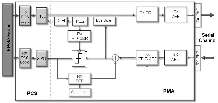
12 Xilinx Transceiver Architecture Overview
13 TX FIR De-emphasis TX IBIS-AMI Model Parameters TXDIFFCTRL: TX swing control, TXPRECURSOR: FIR pre-cursor, TXPOSTCURSOR: FIR post-cursor, TX FIR Equalization Example TXPRECURSOR = 6. TXPOSTCURSOR = 14.
 UT = h1 (DFE first tap) VP")
14 RX IBIS-AMI Model Parameters GTY RX EQ overview and terminology CTLE1 = KH CTLE2 = KL VP = h0 (error slicer level) UT = h1 (DFE first tap) VP VP
15 IBIS-AMI Simulation Flow Highlights
16 IBIS-AMI Model Vs. EDA Tools EDA tools compute the channel impulse response (including package, link channel(s), TX and RX IBIS portion). EDA tools send the ideal waveform to TX AMI model. TX AMI output data is convolved with the cascaded channel impulse response by EDA tools before the data is send to the RX model. RX AMI processes the received signal (equalization and time recovery, etc.) and sends the output to EDA tools. EDA tools do statistical post processing analysis (bathtub curves, eye diagram, BER contours, etc.) over the RX AMI output data.
 log10(ber) Data")


 x 10-11 -0.")


17 Time-Domain Simulation Data Flow Amplitude (AU) log10(ber) Data pattern oversampled by SPB TX GetWave Data pattern oversampled by SPB In-phase Signal Time (s) x x Sampling Point (UI/64) Signal at data sampler Clock ticks RX GetWave = Signal at RX input
18 Clock Ticks Clock ticks represent the adapted CDR sampling phase. They are the output from RX GetWave function. Xilinx transceiver IBIS-AMI models have an Rx AMI parameter to enable or disable clock ticks, while clock ticks are always available. Clock ticks are a function of time/bit sequence, i.e., the separation between two neighboring ticks are not always 1 UI apart. CDR sampling phase is not necessarily (not guaranteed) at the center of the eye, thus Disabling clock ticks and relying on EDA s retiming is often incorrect. CDR sampling phase depends on simulation specific conditions and/or the CDR architecture used in the SerDes design.
19 EDA Tool User Interface Highlights
20 EDA Tools User Interface All but one EDA tool are schematic based. For frequent users, both netlist and schematic interfaces are desired. Running simulations in command line, automation, etc Most tools are successful in incorporating all simulation and model parameters in a simple interface. Some tools still lack intuitiveness when setting important simulation parameters that can impact simulation results. Some jitter and noise parameters are not incorporated in the user interface input.
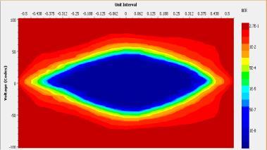
21 EDA Tools Results Viewers Channel characterization results, such as impulse response, are not easily available in some tools. In many cases the user has to enable a debug parameter in order to obtain these outputs. For eye diagrams, some tools have the ability to plot at different BER levels. The user has to be mindful when doing visual inspection. In some tools eye measurements (eye height and eye width) at a specific BER are not provided as part of the results. For these particular tools, the user needs to derive the measurements using the bathtub curves and using simple math. User must be careful when doing manual measurement on bathtub curves.
22 Eye Height Manual Computation Step 1: Generate voltage (vertical) bathtub curve at the given BER, for example, at 1e-10. Step 2: Measure the upper and lower EH, UEH (red) and LEH (green). Step 3: Compute EH based on EH = 2 x min{ueh, LEH}.
23 Eye Width Manual Computation Step 1: Generate time (horizontal) bathtub curve at the given BER, for example, at 1e-10. Step 2: Measure the right and left EW, REW (red) and LEW (green). Step 3: Compute EW based on EW = 2 x min{rew, LEW}.
24 EDA Tool Simulation of Three Cases
25 Simulation Cases Description Case 1 25 Gbps serial link IBIS-AMI simulation with no jitter or noise impairments added to the analysis. Case 2 25 Gbps serial link IBIS-AMI simulation with jitter and noise impairments added to the analysis. Case 3 25 Gbps serial link IBIS-AMI simulation with crosstalk, jitter and noise impairments added to the analysis.
26 Simulation Case 1 25Gbps Thru Channel Simulation Without Jitter or Noise Impairments
27 Simulation Configuration for Case 1 Simulation Setup Data Rate: 25Gbps Pattern: PRBS-15 Samples Per Bit: 64 AMI Processing Block size: 4,096 Ignore Bits: 250E3 Recording Bits: 1E6 EDA Configuration AMI Model Specific TX RX TX RX RJ 0 DJ 0 DCD 0 - RJ 0 DJ 0 DCD 0 RN 0 TXPVT 0 TXDIFFCTRL 31 TXPRECURSOR 6 TXPOSTCURSOR 14 RXPVT 0 DFE Auto-Adapt Enabled CTLE Auto-Adapt Enabled AGC Auto-Adapt Enabled
28 Thru Channel Link Channel Description Data measured with Keysight N5245A S4P Touchstone File v1.0 Frequency range: 10MHz to 40GHz Frequency step: ~3.124MHz

29 Channel IPR (Impulse Response) Impulse Response is defined as the response (output) from a system when an impulse is the input. Generally, Input System Response When the impulse is the input to a system, the output becomes the impulse response. Impulse System Impulse Response The impulse response fully characterizes a LTI system. Most PCB (line cards, backplanes, etc.) and cables can be treated as LTI system. Once the impulse response and the input signal are known, the output of the system is obtained simply by taking the convolution of the input and the impulse response.


30 Channel IPR Generated by EDA Tools
31 IPR to THRU Channel Insertion Loss IPR from EDA-2 looks smooth and has the most commonality with other EDAs. We computed the THRU channel insertion loss and compared it with the original one. The match is reasonable.
32 Observations in Generated Channel IPR s The following are observed from the generated impulse responses Channel IPRs do not look the same: some are smooth, some are rugged; some small, some big; one has more delay than the others. EDA-1 s IPR looks the most rugged, and EDA-6 is the next most rugged. EDA-3 s IPR magnitude is much smaller (~20%) than the rest and has a different profile. EDA-3 s IPR also has a tail that decays more slowly than the rest. EDA-6 s IPR delay is much longer ( >UI/4 at 25Gbps) than the rest. If IPR was truly used in generating channel output waveforms, its magnitude would affect adaptation, and its delay would affect CDR locking phase. It is noticed that eye diagrams do not quite show the differences; this is largely due to the fact that adaptations drive the equalized waveform to the same target. The differences in IPR magnitude or profile are more of a concern to the end users. System margin could be miscalculated without notice.
33 Output Eye Diagrams at BER 1e-6 EDA-1 EDA-2 EDA-3 EDA-4 EDA-5 EDA-6 Color mapping scheme could affect eye appearance
34 Eye Diagram Observations for Case 1 EDAs EDA-1 EDA-2 EDA-3 EDA-4 EDA-5 EDA-6 Outer Eye Smallest Largest Inner Eye Smallest Largest All look similar Eye Shape The outermost traces bifurcated

35 Eye BER = 1e-12 for Case 1
36 CDR Adaptations for Case 1 EDA-1 EDA-2 EDA-3 EDA-4 EDA-5 EDA-6
37 CTLE & AGC Adaptation for Case 1 EDA-1 EDA-2 EDA-3 EDA-4 EDA-5 EDA-6

38 DFE Adaptations for Case 1 EDA-1 EDA-2 EDA-3 EDA-4 EDA-5 EDA-6
39 More Observations for Case 1 EDAs EDA-1 EDA-2 EDA-3 EDA-4 EDA-5 EDA-6 AGC CTLE VP (h0) ~100 ~100 ~102 ~100 ~100 ~100 UT (h1) ~48 ~41 ~55 ~43 ~41 ~43 h2 ~14 ~12 ~14 ~12 ~13 ~12 h3 ~41 ~39 ~43 ~39 ~40 ~40 CDR ~62 ~62 ~38 ~62 ~61 ~77 1e-12 Smallest Largest 1e-12 Smallest Largest
40 Discussion on Case 1 Simulation Results CDR adaptations EDA-3 s CDR results are not expected from its IPR s delay. EDA-6 s CDR is ~25% UI delayed, matching its IPR s delay compared with IPRs from other EDAs. CTLE adaptations All six EDAs yielded similar convergence. AGC adaptations Out of six EDAs, four resulted in AGC=24, one (EDA-1) in AGC=25, and one (EDA-3) in AGC=26. EDA-3 s AGC adaptation result is likely due to its smaller IPR magnitude.
41 Discussion on Case 1 Simulation Results (Con t) DFE tap adaptations VP adaptation results are almost identical among all six EDAs. For UT tap, four EDAs (2, 4, 5, 6) yielded about 41~43. EDA-1 generated a slightly larger value, about 48. EDA-3 produced a larger UT tap value, about 55 (related to IPR shape). EDA-3 produced a larger h2 tap value (related to IPR shape). Eye metrics (EH and EW at BER=1e-12) EDA-5 is on the most pessimistic side, smallest in both EH and EW. EDA-6 is on the most optimistic side, largest in both EH and EW. EDA-1, EDA-2, EDA-3, EDA-4 have similar EH and EW.

42 Simulation Time Comparison Simulation time is recorded for a total of 1.25M bits, for Case 1 Simulation time includes channel IPR characterization; Five out of six EDAs showed a total simulation less than 10 min for 1.25M bits; EDA-2 showed about 6x longer time. It is believed that a lot of time was spent on IPR generation.
43 Simulation Cases Description Case 1 25 Gbps serial link IBIS-AMI simulation with no jitter or noise impairments added to the analysis. Case 2 25 Gbps serial link IBIS-AMI simulation with jitter and noise impairments added to the analysis. Case 3 25 Gbps serial link IBIS-AMI simulation with crosstalk, jitter and noise impairments added to the analysis.
44 Simulation Case 2 25Gbps Thru Channel Simulation With Jitter and Noise Impairments
45 Simulation Configuration for Case 2 Simulation Setup Data Rate: 25Gbps Pattern: PRBS-15 Samples Per Bit: 64 AMI Processing Block size: 4,096 Ignore Bits: 250E3 Recording Bits: 1E6 EDA Configuration AMI Model Specific TX RX TX RX RJ 0.01 UI DJ 0.04 UI DCD 0.02 UI - RJ 0.01 UI DJ UI DCD 0.01 UI RN 2.5mV TXPVT 0 TXDIFFCTRL 31 TXPRECURSOR 6 TXPOSTCURSOR 14 RXPVT 0 DFE Auto-Adapt Enabled CTLE Auto-Adapt Enabled AGC Auto-Adapt Enabled
46 Link Channel Description Thru Channel Data measured with Keysight N5245A S4P Touchstone File v1.0 Frequency range: 10MHz to 40GHz Frequency step: ~3.124MHz
47 Output Eye Diagrams at BER 1e-6 EDA-1 EDA-2 EDA-3 EDA-4 EDA-5 EDA-6 Color mapping scheme could affect eye appearance
48 Eye Diagram Observations for Case 2 EDAs EDA-1 EDA-2 EDA-3 EDA-4 EDA-5 EDA-6 Outer Eye Largest Smallest Inner Eye Smallest Largest All look similar Eye Shape The outermost traces bifurcated

49 Eye Metrics at BER = 1e-12 for Case 2

 EDA-4")
50 BER Contours for Case 2 EDA-1 EDA-2 EDA-3 (BER 1e-9) BER Contours (BER 1e-12, 1e-15, 1e-21) EDA-4 EDA-5 EDA-6
51 Timing Bathtub Curves for Case 2
52 CDR Adaptations for Case 2 EDA-1 EDA-2 EDA-3 EDA-4 EDA-5 EDA-6
53 CTLE & AGC Adaptation for Case 2 EDA-1 EDA-2 EDA-3 EDA-4 EDA-5 EDA-6

54 DFE Adaptations for Case 2 EDA-1 EDA-2 EDA-3 EDA-4 EDA-5 EDA-6
55 More Observations for Case 2 EDAs EDA-1 EDA-2 EDA-3 EDA-4 EDA-5 EDA-6 AGC CTLE VP (h0) ~100 ~99 ~100 ~100 ~100 ~100 UT (h1) ~48 ~57 ~56 ~43 ~41 ~41 h2 ~13 ~16 ~17 ~13 ~13 ~13 h3 ~40 ~41 ~42 ~40 ~40 ~40 CDR ~61 ~58 ~38 ~61 ~61 ~77 1e-12 Smallest NA Largest 1e-12 Smallest NA Largest
56 Discussion on Case 2 Simulation Results CDR adaptations EDA-2 CDR adaptation result is unexpectedly affected; it locked about 1/16 UI earlier than that in Case 1. CTLE adaptations All six EDAs generated approximately CTLE=20 (same as those in Case 1). AGC adaptations EDA-1 remains unchanged from Case 1, converged to 25. EDA-4, EDA-5 and EDA-6 remain unchanged from Case 1, at 24. EDA-3 convergence is slightly reduced from 26 to 25. EDA-2 is unexpectedly reduced from 24 to 16, which is an outlier.
57 Discussion on Case 2 Simulation Results (Con t) DFE tap adaptations EDA-2 has UT and DFE tap noticeably changed, which is an outlier. Eye metrics (EH and EW at BER=1e-12) We could not generate EH or EW from EDA-2, as of this date. EDA-1 has the most EH and EW reduction, compared with Case 1. EDA-3 has the least EH reduction, compared with Case 1. EDA-5 has the least EW reduction, compared with Case 1. Bathtub curves The six EDAs generated very different bathtub curves, including curve slopes. We could not extrapolate beyond 1e-6 in EDA-2, so the EH/EW data it is left blank. The conclusion for system margin could be different using different EDA tools.
58 Simulation Cases Description Case 1 25 Gbps serial link IBIS-AMI simulation with no jitter or noise impairments added to the analysis. Case 2 25 Gbps serial link IBIS-AMI simulation with jitter and noise impairments added to the analysis. Case 3 25 Gbps serial link IBIS-AMI simulation with crosstalk, jitter and noise impairments added to the analysis.
59 Simulation Case 3 25Gbps Crosstalk Channel Simulation With Jitter and Noise Impairments
60 Simulation Configuration for Case 3 Simulation Setup Data Rate: 25Gbps Data Pattern: PRBS-15 Samples Per Bit: 64 AMI Processing Block size: 4,096 Ignore Bits: 250E3 Recording Bits: 1E6 Crosstalk Aggressors Data Rate: 25Gbps EDA Configuration AMI Model Specific TX RX TX RX RJ 0.01 UI DJ 0.04 UI DCD 0.02 UI - Pattern: PRBS-13 RJ 0.01 UI DJ UI DCD 0.01 UI RN 2.5mV TX Phase: 0 TXPVT 0 TXDIFFCTRL 31 TXPRECURSOR 6 TXPOSTCURSOR 14 RXPVT 0 DFE Auto-Adapt Enabled CTLE Auto-Adapt Enabled AGC Auto-Adapt Enabled TX model specific parameters are the same as those for the victim
61 Thru Channel Link Channel Description Data measured with Keysight N5245A. S12P Touchstone File v1.0. Frequency range: 10MHz to 40GHz. Frequency step: ~3.124MHz. Crosstalk Channels Format is same as that for the THRU. The ICN from the aggressors is about 1.97mV rms. (The simulation is carried out in time domain.)
62 Output Eye Diagrams at BER 1e-6 EDA-1 EDA-2 EDA-3 EDA-4 EDA-5 EDA-6 Color mapping scheme could affect eye appearance
63 Eye Diagram Observations for Case 3 EDAs EDA-1 EDA-2 EDA-3 EDA-4 EDA-5 EDA-6 Outer Eye Smallest Largest Inner Eye Smallest Largest All look similar Eye Shape The outermost traces bifurcated

64 Eye Metrics at BER = 1e-12 for Case 3
 EDA-4 EDA-5")
65 BER Contours for Case 3 EDA-1 EDA-2 EDA-3 (BER 1e-9) BER Contours (BER 1e-12, 1e-15, 1e-21) EDA-4 EDA-5 EDA-6
66 Timing Bathtub Curves for Case 3
67 More Observations for Case 3 EDAs EDA-1 EDA-2 EDA-3 EDA-4 EDA-5 EDA-6 AGC CTLE VP (h0) ~100 ~100 ~99 ~100 ~100 ~100 UT (h1) ~48 ~42 ~54 ~43 ~41 ~41 h2 ~15 ~13 ~16 ~15 ~14 ~15 h3 ~40 ~40 ~42 ~40 ~40 ~40 CDR ~62 ~62 ~38 ~62 ~61 ~77 1e-12 Largest Smallest 1e-12 Largest Smallest
68 CDR Adaptations for Case 3 EDA-1 EDA-2 EDA-3 EDA-4 EDA-5 EDA-6
69 CTLE & AGC Adaptation for Case 3 EDA-1 EDA-2 EDA-3 EDA-4 EDA-5 EDA-6
70 DFE Adaptations for Case 3 EDA-1 EDA-2 EDA-3 EDA-4 EDA-5 EDA-6
71 Discussion on Case 3 Simulation Results CDR adaptations CDR behaviors are matching Case 1, which is the expected behavior. CTLE adaptations All six EDAs generated approximately CTLE=20 (same as those in both Case 1 and Case 2). AGC adaptations Except for EDA-3, AGC adaptations match Case 1, the expected behavior. EDA-3 AGC slightly reduced from 26 to 25, compared with that in Case 1, and matching that in Case 2. EDA-2 AGC now matched that in Case 1, still making Case 2 an outlier.
72 Discussion on Case 3 Simulation Results (Con t) DFE tap adaptations Except for EDA-3, DFE adaptations match Case 1 only with increased variations, which is the expected behavior. EDA-3 results match Case 2. Eye metrics (EH and EW at BER=1e-12) We could not generate the data in EDA-2 for this measurement. EDA-3 stood out; it generated the largest EH, and the largest EW. EDA-3, somehow, showed increased EH and EW, compared with Case 2. Bathtub curves The six EDAs generated very different bathtub curves, including curve slopes. We could not extrapolate beyond 1e-6 in EDA-2, thus data it is left blank. The conclusion for system margin could be different using different EDA tools.
73 Selected Comparison of Simulation Results
74 Case 1: No added jitter or noise Comparison of Eye Diagrams EDA-1 EDA-2 EDA-3 EDA-4 EDA-5 EDA-6 Case 2: With added jitter and noise Case 3: With added jitter and noise, plus crosstalk

75 Comparison of Eye Height (mv) at 1e-12 With no added jitter or noise With added jitter and noise With added jitter, noise, and Xtalk
76 Eye Height Change Between Cases Eye Height Reduction (%) From Case 1 to Case 2 From Case 2 to Case 3 From Case 1 to Case 3 EDA EDA EDA EDA EDA EDA

77 With no added jitter or noise Comparison of Eye Width (ps) at 1e-12 With added jitter and noise With added jitter, noise, and Xtalk
78 Eye Width Change Between Cases Eye Width Reduction (%) From Case 1 to Case 2 From Case 2 to Case 3 From Case 1 to Case 3 EDA EDA EDA EDA EDA EDA
79 Comparison of Timing Bathtub Curves Without Crosstalk (Case 2) With Crosstalk (Case 3)
80 Bathtub Curves w/o (blue) & w/ (red) Crosstalk
81 Bathtub Curves w/o (blue) & w/ (red) Crosstalk Only EDA-5 and EDA-6 showed consistent degradation for both sides. EDA-2 showed larger EW, for both left and right side, even at BER = 1e-6. EDA-3 and EDA-4 showed a shift of the sides to the right. EDA-1 showed a shift of bathtub curve to the left side.

82 Eye Width Vs. Timing Bathtub for Case 2 The bar chart of eye width is derived from the timing bathtub curves.
83 Eye Width Vs. Timing Bathtub for Case 3 The bar chart of eye width is derived from the timing bathtub curves.
84 VP (h0) Adaptations for Case 3

85 DFE UT (h1) Adaptations for Case 3

86 DFE h2 Adaptations for Case 3
87 AGC Adaptations for Case 3
88 CDR Adaptations for Case 3

89 Baseline Wander Correction for Case 3

90 Comparing Eye Height from Bathtub Curve for EDA-3 between Case 2 and Case 3 Case 2 and Case 3 crosses over at ~BER=1e-10. Since EH is determined by the smaller side of the branch, the left branch dominates in this example. The left branch showed less slope when crosstalk is added (Case 3) than in Case 2, which is not expected.
91 Summary of the Work
92 Summary Six EDAs are used to perform link simulations, based on Xilinx UltraScale GTY IBIS-AMI model (V2.1), of three setup conditions: (1) the THRU channel only without added noise or jitter, (2) with added noise and jitter, and (3) plus crosstalk interference, all at 25Gbps with a ~25dB loss backplane channel, whose model was provided by a Xilinx key customer. During the process of working on the above simulations, we have engaged proactively with all the six involved EDAs, trying to make sure our operations are intended and our setups are correct. However, we cannot guarantee that our presented results and our understanding of tool configurations always reflect the EDA intensions. In fact, a couple EDAs made quite a few changes during the work. The result in this presentation represent the latest information available to us.
93 Summary (Con t 1) In general, the differences in tools capabilities and in certain results are quite large, larger than we initially anticipated. Xilinx is happy to work with any EDAs to investigate any unexpected results. Xilinx is also willing to assist any EDAs to find the cause of any discrepancies, be that the impulse response, the adaptation convergences, available EDA output parameters, or post-processing results. For the discrepancies that were observed, first, some EDAs have different IPR results, which surely affect link performance judgments: Although the impact might not be visible from eye diagrams or bathtub curves, it can be revealed from converged parameter adaptation results. EDA-6 delay in IPR translates into delay in CDR sampling phase. EDA-3 has a different IPR profile but its impact on CDR adaptation is unexpected.
94 Summary (Con t 2) Although using identical SerDes TX and RX IBIS-AMI models, as well as the same channel s-parameter file(s), we have not seen any two EDAs generated the same data for any of the three simulated cases. For example, for DFE h1 tap, the differences could be 16 codes among the six EDA results; for AGC, the difference could be 12 in settings, etc. EDAs have varying approaches in BER extrapolation, which could lead to drastically different conclusions regarding system margin. Different extrapolation methods also yielded different bathtub curve slopes. When jitter/noise and crosstalk are added, converged adaptations are not expected to deviate by a lot. This is generally true for all EDAs. The only exception is with EDA-2 in Case 2, which was unexpected.
95 Summary (Con t 3) When jitter/noise are added (Case 2), all EDAs show reduced EH and EW, i.e., less link performance margin, as expected. However, when crosstalk is introduced (Case 3), four EDAs showed further reduced EH and EW (from Case 2), as expected, but EDA-3 yielded both increased EH and EW. EDA-4 showed increased EW as well. Some EDAs showed very small amount of reduction (EDA-1), while others showed huge degradation (EDA-5). In conclusion, we have learned a lot from this work. We will keep working with EDAs to understand the unexpected and inconsistent results, such that we can better address our customers inquires and concerns.

96 Xilinx would like to thank all the six EDAs for their help with using the tools and discussions of the results!
IBIS-AMI Modeling and Simulation of 56G PAM4 Link Systems
 IBIS-AMI Modeling and Simulation of 56G PAM4 Link Systems Hongtao Zhang, hongtao@xilinx.com Fangyi Rao, fangyi_rao@keysight.com Xiaoqing Dong, dongxiaoqing82@huawei.com Geoff Zhang, geoffz@xilinx.com Outline
Predicting BER with IBIS-AMI: experiences correlating SerDes simulations and measurement
 Predicting BER with IBIS-AMI: experiences correlating SerDes simulations and measurement Todd Westerhoff (SiSoft) Mike Steinberger (SiSoft) Walter Katz (SiSoft) Barry Katz (SiSoft) Adge Hawes (IBM) Kent
An Overview of High-Speed Serial Bus Simulation Technologies
 An Overview of High-Speed Serial Bus Simulation Technologies Asian IBIS Summit, Beijing, China September 11, 27.25.2.15.1.5 -.5 -.1 Arpad Muranyi arpad_muranyi@mentor.com Vladimir Dmitriev-Zdorov -.15
SerDes Channel Simulation in FPGAs Using IBIS-AMI
 White Paper: Virtex-6 FPGA Family WP382 (v10) December 9, 2010 SerDes Channel Simulation in FPGAs Using IBIS-AMI By: Romi Mayder The IBIS Algorithmic Modeling Interface (IBIS-AMI) was developed to enable
Proposal for modeling advanced SERDES
 Proposal for modeling advanced SERDES IBM, Cadence June 2006 1 CADENCE DESIGN SYSTEMS, INC. Presenters, Contributors Presenters / Contributors 1. Joe Abler IBM Systems & Technology Group High Speed Serial
Keysight Technologies IBIS-AMI Based Link Analysis of Realistic 56G PAM4 Channels
 Keysight Technologies IBIS-AMI Based Link Analysis of Realistic 56G PAM4 Channels White Paper This white paper was first published at DesignCon in January, 2016. Reprinted with permission from DesignCon.
5 GT/s and 8 GT/s PCIe Compared
 5 GT/s and 8 GT/s PCIe Compared Bent Hessen-Schmidt SyntheSys Research, Inc. Copyright 2008, PCI-SIG, All Rights Reserved 1 Disclaimer The material included in this presentation reflects current thinking
Using IBIS-AMI in the Modeling of Advanced SerDes Equalization for Serial Link Simulation
 Using IBIS-AMI in the Modeling of Advanced SerDes Equalization for Serial Link Simulation CDNLive Boston August 2013 Mark Marlett and Mahesh Tirupattur, Analog Bits Ken Willis and Kumar Keshavan, Cadence
Advanced Jitter Analysis with Real-Time Oscilloscopes
 with Real-Time Oscilloscopes August 10, 2016 Min-Jie Chong Product Manager Agenda Review of Jitter Decomposition Assumptions and Limitations Spectral vs. Tail Fit Method with Crosstalk Removal Tool Scope
100GEL C2M Channel Analysis Update
 100GEL C2M Channel Analysis Update Jane Lim, Cisco Pirooz Tooyserkani, Cisco Upen Reddy Kareti, Cisco Joel Goergen, Cisco Marco Mazzini, Cisco 9/5/2018 IEEE P802.3ck 100Gb/s, 200Gb/s, and 400Gb/s Electrical
SerDes Modeling: IBIS-ATM & Model Validation July 2007
 SerDes Modeling: IBIS-ATM & Model Validation July 2007 Signal Integrity Software, Inc. IBIS-ATM Effort Goal: SerDes Rx/TX model interoperability Multiple EDA environments Multiple SerDes vendor models
Explore your design space including IBIS AMI models with Advanced Channel Simulation
 Explore your design space including IBIS AMI models with Advanced Channel Simulation Heidi Barnes Vincent Poisson Presenter: May, 2013 Agenda How good is my PHY? Channel Simulation Options Spice (Circuit
Leveraging IBIS Capabilities for Multi-Gigabit Interfaces. Ken Willis - Cadence Design Systems Asian IBIS Summit, Shanghai, PRC November 13, 2017
 Leveraging IBIS Capabilities for Multi-Gigabit Interfaces Ken Willis - Cadence Design Systems Asian IBIS Summit, Shanghai, PRC November 13, 2017 Overview In writing EDI CON paper Signal Integrity Methodology
Understanding IBIS-AMI Simulations
 Understanding IBIS-AMI Simulations Agenda IBIS-AMI Assumptions & Terminology IBIS-AMI Model Components Analysis Stages & Simulation Types Algorithmic Model Types Static and Dynamic Equalization IBIS-AMI
Application Note. PCIE-RA Series Final Inch Designs in PCI Express Applications Generation GT/s
 PCIE-RA Series Final Inch Designs in PCI Express Applications Generation 3-8.0 GT/s Copyrights and Trademarks Copyright 2012, Inc. COPYRIGHTS, TRADEMARKS, and PATENTS Final Inch is a trademark of, Inc.
A New Method For Developing IBIS-AMI Models
 A New Method For Developing IBIS-AMI Models Hongtao Zhang, hongtao@xilinx.com John Baprawski, john.baprawski@gmail.com Pegah Alavi, pegah_alavi@keysight.com Geoff Zhang, geoffz@xilinx.com Executive Summary
Application Note. PCIE-EM Series Final Inch Designs in PCI Express Applications Generation GT/s
 PCIE-EM Series Final Inch Designs in PCI Express Applications Generation 3-8.0 GT/s Copyrights and Trademarks Copyright 2015, Inc. COPYRIGHTS, TRADEMARKS, and PATENTS Final Inch is a trademark of, Inc.
SPISim StatEye/AMI User s Guide
 SPISim StatEye/AMI User s Guide Latest Version: V20180315 SPISim LLC Vancouver, WA 98683, USA Tel. +1-408-905-6692 http://www.spisim.com This user s guide describes the SPISim s StatEye channel analysis
Simulation Results for 10 Gb/s Duobinary Signaling
 Simulation Results for 10 Gb/s Duobinary Signaling Populating the Signaling Ad Hoc Spreadsheet IEEE 802.ap Task Force Atlanta March 15-17, 2005 802.AP Backplane Ethernet Contributors Vitesse Majid Barazande-Pour
PCI Express Electrical Basics
 PCI Express Electrical Basics Dean Gonzales Advanced Micro Devices Copyright 2015, PCI-SIG, All Rights Reserved 1 Topics PCI Express Overview Enhancements for 8GT/s Target Channels for the Specification
DisplayPort 1.4 Webinar
 DisplayPort 1.4 Webinar Test Challenges and Solution Yogesh Pai Product Manager - Tektronix 1 Agenda DisplayPort Basics Transmitter Testing Challenges DisplayPort Type-C Updates Receiver Testing Q and
SEAM-RA/SEAF-RA Series Final Inch Designs in PCI Express Applications Generation GT/s
 SEAM-RA/SEAF-RA Series Final Inch Designs in PCI Express Applications Generation 3-8.0 GT/s Copyrights and Trademarks Copyright 2011 Samtec, Inc. Developed in conjunction with Teraspeed Consulting Group
Measurement and Simulation of a High- Speed Electro/Optical Channel
 TITLE Measurement and Simulation of a High- Speed Electro/Optical Channel Shirin Farrahi, (Oracle) Image Michael Cina (TE Connectivity), Jeffery Marquart (TE Connectivity), Andrei Kaikkonen (TE Connectivity),
UNDERSTANDING IBIS-AMI SIMULATIONS
 UNDERSTANDING IBIS-AMI SIMULATIONS Track 6, Session TH4 Douglas Burns dburns@sisoft.com John Madsen jmadsen@sisoft.com Signal Integrity Software, Inc. Signal Integrity Software, Inc. Todd Westerhoff Signal
RiseUp RU8-DP-DV Series 19mm Stack Height Final Inch Designs in PCI Express Applications. Revision Date: March 18, 2005
 RiseUp RU8-DP-DV Series 19mm Stack Height Final Inch Designs in PCI Express Applications Revision Date: March 18, 2005 Copyrights and Trademarks Copyright 2005 Samtec, Inc. Developed in conjunction with
Understanding IBIS-AMI Simulations
 Understanding IBIS-AMI Simulations IBIS European Summit SPI, Turin, Italy May 11, 2016 Richard Allred, Signal Integrity Software Agenda IBIS-AMI Assumptions & Terminology IBIS-AMI Model Components Analysis
PCI Express Link Equalization Testing 서동현
 PCI Express Link Equalization 서동현 Application Engineer January 19th, 2016 Agenda Introduction Page 2 Dynamic Link Equalization TX/RX Link Equalization Tests Test Automation RX Stress Signal Calibration
AMI Applications in High-speed Serial Channel Analysis and Measurement Correlation
 AMI Applications in High-speed Serial Channel Analysis and Measurement Correlation Jia Wei, Sunanbing, Zhu ShunLin Jia.wei@zte.com.cn, sun.anbing@zte.com.cn, Zhu.shunlin@zte.com.cn High-Speed System Lab,ZTE
ADS USB 3.1 Compliance Test Bench
 ADS 2016.01 USB 3.1 Compliance Test Bench Notices Keysight Technologies, Inc. 1983-2016 1400 Fountaingrove Pkwy., Santa Rosa, CA 95403-1738, United States All rights reserved. No part of this documentation
PCIEC PCI Express Jumper High Speed Designs in PCI Express Applications Generation GT/s
 PCIEC PCI Express Jumper High Speed Designs in PCI Express Applications Generation 3-8.0 GT/s Mated with PCIE-RA Series PCB Connectors Copyrights and Trademarks Copyright 2015, Inc. COPYRIGHTS, TRADEMARKS,
Q Pairs QTE/QSE-DP Final Inch Designs In PCI Express Applications 16 mm Stack Height
 Application Note Q Pairs QTE/QSE-DP Final Inch Designs In PCI Express Applications 16 mm Stack Height Copyrights and Trademarks Copyright 2004 Samtec, Inc. Developed in conjunction with Teraspeed Consulting
IBIS-ATM Update: SerDes Modeling and IBIS
 IBIS-ATM Update: SerDes Modeling and IBIS (Originally presented at the Sept 11 th Summit in Beijing) Presented by: Todd Westerhoff, SiSoft twesterh@sisoft.com IBIS Summit Tokyo, Japan September 14, 2007
A Practical Methodology for SerDes Design
 A Practical Methodology for SerDes Design Asian IBIS Summit, Shanghai, China, November 14, 2018 Authors: Amy Zhang, Guohua Wang, David Zhang, Zilwan Mahmod, Anders Ekholm agenda Challenges in Traditional
Maximising Serial Bandwidth And Signal Integrity In FPGAs
 Maximising Serial Bandwidth And Signal Integrity In FPGAs Francesco Contu High Speed IO specialist, EMEA South francescocontu@xilinxcom Agilent High Speed Digital Design & Validation Seminars 2012 Agenda
Keysight Technologies EZJIT Plus Jitter Analysis Software for Infiniium Oscilloscopes. Data Sheet
 Keysight Technologies EZJIT Plus Jitter Analysis Software for Infiniium Oscilloscopes Data Sheet 02 Keysight EZJIT Plus Jitter Analysis Software for Infiniium Oscilloscopes - Data Sheet Table of Contents
Agilent Technologies EZJIT and EZJIT Plus Jitter Analysis Software for Infiniium Series Oscilloscopes
 Agilent Technologies EZJIT and EZJIT Plus Jitter Analysis Software for Infiniium Series Oscilloscopes Data Sheet Features of the EZJIT Plus software that optimize jitter analysis include: Easy-to-use jitter
10GBASE-KR for 40G Backplane
 1GBASE-KR for 4G Backplane Nov 7 Technology Hiroshi Takatori Hiroshi.Takatori@.us 1 Outline This contribution discusses, - Performance based on 1GBASE-KR Std - Theoretical Limit (Saltz SNR) and Time Domain
PCI Express 3.0 Characterization, Compliance, and Debug for Signal Integrity Engineers
 PCI Express 3.0 Characterization, Compliance, and Debug for Signal Integrity Engineers - Transmitter Testing - Receiver Testing - Link Equalization Testing David Li Product Marketing Manager High Speed
Optimal Management of System Clock Networks
 Optimal Management of System Networks 2002 Introduction System Management Is More Challenging No Longer One Synchronous per System or Card Must Design Source-Synchronous or CDR Interfaces with Multiple
An Innovative Simulation Workflow for Debugging High-Speed Digital Designs using Jitter Separation
 An Innovative Simulation Workflow for Debugging High-Speed Digital Designs using Jitter Separation C. Chastang, A. Amédéo V. Poisson, P. Grison, F. Demuynck C. Gautier, F. Costa Thales Communications &
Q2 QMS/QFS 16mm Stack Height Final Inch Designs In PCI Express Applications Generation Gbps. Revision Date: February 13, 2009
 Q2 QMS/QFS 16mm Stack Height Final Inch Designs In PCI Express Applications Generation 2 5.0 Gbps Revision Date: February 13, 2009 Copyrights and Trademarks Copyright 2009 Samtec, Inc. Developed in conjunction
Concerns when applying Channel Simulation to DDR4 Interface
 Concerns when applying Channel Simulation to DDR4 Interface Masaki Kirinaka mkirinaka@jp.fujitsu.com Akiko Tsukada tsukada.akiko@jp.fujitsu.com FUJITSU INTERCONNECT TECHNOLOGIES LIMITED Asian IBIS Summit
AN 608: HST Jitter and BER Estimator Tool for Stratix IV GX and GT Devices
 AN 608: HST Jitter and BER Estimator Tool or Stratix IV GX and GT Devices July 2010 AN-608-1.0 The high-speed communication link design toolkit (HST) jitter and bit error rate (BER) estimator tool is a
Serial Link Analysis and PLL Model
 25. July 2007 Serial Link Analysis and PLL Model September 11, 2007 Asian IBIS Summit, Beijing China Huang Chunxing huangchunxing@huawei.com www.huawei.com HUAWEI TECHNOLOGIES Co., Ltd. Agenda High-speed
PCI Express 4.0. Electrical compliance test overview
 PCI Express 4.0 Electrical compliance test overview Agenda PCI Express 4.0 electrical compliance test overview Required test equipment Test procedures: Q&A Transmitter Electrical testing Transmitter Link
IBIS-AMI: Assumptions, Terminology & Analytical Flows
 IBIS-AMI: Assumptions, Terminology & Analytical Flows Walter Katz (wkatz@sisoft.com) Mike Steinberger (msteinb@sisoft.com) Todd Westerhoff (twesterh@sisoft.com) SiSoft DesignCon IBIS Summit February 3,
Building IBIS-AMI Models for DDR5 Applications. Todd Westerhoff, SiSoft
 Building IBIS-AMI Models for DDR5 Applications Todd Westerhoff, SiSoft SPEAKERS Image Todd Westerhoff VP, Semiconductor Relations, SiSoft twesterh@sisoft.com www.sisoft.com Todd has over 37 years of experience
MECT Series Final Inch Designs in SFP+ Applications. Revision Date: August 20, 2009
 MECT Series Final Inch Designs in SFP+ Applications Revision Date: August 20, 2009 Copyrights and Trademarks Copyright 2009 Samtec, Inc. Developed in conjunction with Teraspeed Consulting Group LLC COPYRIGHTS,
QPairs QTE/QSE-DP Multi-connector Stack Designs In PCI Express Applications 16 mm Connector Stack Height REVISION DATE: OCTOBER 13, 2004
 Application Note QPairs QTE/QSE-DP Multi-connector Stack Designs In PCI Express Applications 16 mm Connector Stack Height REVISION DATE: OCTOBER 13, 2004 Copyrights and Trademarks Copyright 2004 Samtec,
High-Speed Jitter Testing of XFP Transceivers
 White Paper High-Speed Jitter Testing of XFP Transceivers By Andreas Alpert Abstract Jitter is a key performance factor in high-speed digital transmission systems, such as synchronous optical networks/synchronous
High Speed Transceiver Debugging NMI FPGA Network 2015 David Taylor Xilinx HSIO AE
 High Speed Transceiver Debugging NMI FPGA Network 2015 David Taylor Xilinx HSIO AE Agenda Transceiver Overview Design for debug Debug tools and methodology practical steps Advanced debug Summary Demo Page
Using RJ45 Category 7 Cabling for 2 Lane, 1 and 2.5Gbps Serial Data Transmission
 Using RJ45 Category 7 Cabling for 2 Lane, 1 and 2.5Gbps Serial Data Transmission Test 8561 (Category 7, 2 lane) J Sawdy, Sr. SI Engineer 4/14/10 Forward The RJ45 connector is found in enterprise installations
Agilent. Master your next PCIe test with the Agilent M8020A High-Performance BERT Application Brief
 Agilent Master your next PCIe test with the Agilent M8020A High-Performance BERT Application Brief 1 Table of Contents Contents Disclaimer... 3 1 Introduction... 4 2 PCI Express Specifications... 4 3 PCI
Characterize and Debug Crosstalk Issues with Keysight Crosstalk Analysis App
 Chong Min-Jie Characterize and Debug Crosstalk Issues with Crosstalk Analysis App Page Characterize and Debug Crosstalk Issues with Crosstalk Analysis App Min-Jie Chong HPS Product Manager & Planner Oscilloscope
Virtex-6 FPGA GTX Transceiver OTU1 Electrical Interface
 Virtex-6 FPGA GTX Transceiver OTU1 Electrical Interface Characterization Report Xilinx is disclosing this user guide, manual, release note, and/or specification (the "Documentation") to you solely for
SAS-2 Zero-Length Test Load Characterization (07-013r7) Barry Olawsky Hewlett Packard (8/2/2007)
 Barry Olawsky Hewlett Packard (8/2/2007)") SAS-2 Zero-Length Test Load Characterization (07-013r7) Barry Olawsky Hewlett Packard (8/2/2007) 07-013r7 SAS-2 Zero-Length Test Load Characterization 1 Zero-Length Test Load Provides ideal connection
SAS-2 Zero-Length Test Load Characterization (07-013r7) Barry Olawsky Hewlett Packard (8/2/2007) 07-013r7 SAS-2 Zero-Length Test Load Characterization 1 Zero-Length Test Load Provides ideal connection
Validation of Quasi-Analytical and Statistical Simulation Techniques for Multi-Gigabit Interconnect Channels
 DesignCon 2010 Validation of Quasi-Analytical and Statistical Simulation Techniques for Multi-Gigabit Interconnect Channels Chad Morgan, Tyco Electronics chad.morgan@tycoelectronics.com, 717-649-4129 Abstract
Comparison of BER Estimation Methods which Account for Crosstalk
 Comparison of BER Estimation Methods which Account for Crosstalk As presented at DesignCon 2009 Co-authored by: Michael Steinberger, Signal Integrity Software, Inc. msteinb@sisoft.com Barry Katz, Signal
Multi-Gigabit Serial Link Analysis using HSPICE and AMI Models
 Multi-Gigabit Serial Link Analysis using HSPICE and AMI Models Douglas Burns Barry Katz Walter Katz Mike Steinberger Todd Westerhoff Signal Integrity Software, Inc. (SiSoft) Maynard, MA, USA www.sisoft.com
Tektronix Innovation Forum
 Tektronix Innovation Forum Enabling Innovation in the Digital Age DisplayPort 1.2 Spec Updates and overview of Physical layer conformance testing Presenter: John Calvin DisplayPort 1.2 Spec Updates Agenda
A Beginner s Guide to SerDes and AMI Modeling. Todd Westerhoff, SiSoft Corey Mathis, MathWorks
 A Beginner s Guide to SerDes and AMI Modeling Todd Westerhoff, SiSoft Corey Mathis, MathWorks SPEAKERS Corey Mathis Industry Marketing Manager, MathWorks Corey.Mathis@mathworks.com, www.mathworks.com Corey
Virtex-6 FPGA GTX Transceiver Characterization Report
 Virtex-6 FPGA GTX Transceiver Characterization Report PCI Express 2.0 (2.5 and 5.0 Gb/s) Electrical Standard Xilinx is disclosing this user guide, manual, release note, and/or specification (the Documentation
Jitter Basics Lab Using SDAIII & Jitter Sim
 Jitter Basics Lab Using SDAIII & Jitter Sim TUTORIAL August 1, 2012 Summary JitterSim is a math function, enabled by the Serial Data Analysis option, which allows various aspects of jitter to be simulated
Automated AMI Model Generation & Validation
 Automated AMI Model Generation & Validation José Luis Pino Amolak Badesha Agilent EEsof EDA Manuel Luschas Antonis Orphanou Halil Civit Asian IBIS Summit, Shenzhen China November 9, 2010 (Presented previously
T10 Technical Committee From: Barry Olawsky, HP Date: 13 January 2005 Subject: T10/05-025r1 SFF8470 Crosstalk Study
 To: T10 Technical Committee From: Barry Olawsky, HP (barry.olawsky@hp.com) Date: Subject: T10/ Revision History Revision 0 (5 January 2005) First revision Revision 1 () Second revision Further clarify
Virtex-5 FPGA RocketIO GTX Transceiver Characterization Report
 Virtex-5 FPGA RocketIO GTX Transceiver Characterization Report PCI Express 2.0 (5.0 Gb/s) Electrical Gb/s) Standard Electrical Standard [optional] [optional] Xilinx is disclosing this user guide, manual,
Gain and Equalization Adaptation to Optimize the Vertical Eye Opening in a Wireline Receiver. D. Dunwell and A. Chan Carusone University of Toronto
 Gain and Equalization Adaptation to Optimize the Vertical Eye Opening in a Wireline Receiver D. Dunwell and A. Chan Carusone University of Toronto Analog Front End Adaptation Analog Front-End (AFE) Digital
Raj Kumar Nagpal, R&D Manager Synopsys. Enabling Higher Data Rates and Variety of Channels with MIPI D-PHY
 Raj Kumar Nagpal, R&D Manager Enabling Higher Data Rates and Variety of Channels with MIPI D-PHY Agenda Design motivation MIPI D-PHY evolution Summary of MIPI D-PHY specification MIPI channel evolution
Feasibility of 40/100G Heterogeneous System based on Channel Data
 Feasibility of 40/100G Heterogeneous System based on Channel Data Jan 2008 Technology Hiroshi Takatori Hiroshi.Takatori@.us 1 Outline Generalized methodology for feasibility analysis of heterogeneous (electro-optical)
SerDes Modeling: Demonstrating IBIS-AMI Model Interoperability
 SerDes Modeling: Demonstrating IBIS-AMI Model Interoperability Todd Westerhoff, SiSoft twesterh@sisoft.com IBIS Summit @ DesignCon 2008 Santa Clara, CA February 7, 2008 Signal Integrity Software, Inc.
Achieving PCI Express Compliance Faster
 Achieving PCI Express Compliance Faster Agenda PCIe Overview including what s new with Gen4 PCIe Transmitter Testing PCIe Receiver Testing Intro to Tektronix s PCIe Tx and Rx Test Solution PCIe Market
100G Signaling Options over Backplane Classes
 100G Signaling Options over Backplane Classes IEEE P802.3bj January 2012 Newport Beach FutureWei Hiroshi Takatori Hiroshi.Takatori@huawei.com Contributors and Supporters Albert Vareljian Sanjay Kasturia,
Two for One: Leveraging SerDes Flows for AMI Model Development
 DesignCon 2016 Two for One: Leveraging SerDes Flows for AMI Model Development Ren Sang Nah, MathWorks RenSang.Nah@mathworks.com Corey Mathis, MathWorks Corey.Mathis@mathworks.com Richard Allred, SiSoft
Provides information for this release. Describes added functions for this release. Describes bug fixes in the released software version.
 ANRITSU CORPORATION 5-1-1 Onna, Atsugi-shi, Kanagawa 243-8555 Japan Anritsu - GRL PCIe 4.0 CEM Rx Test Application Release Note First Edition This software is released for PCIe CEM Rx Test. Table of Contents
Signal Integrity Analysis for 56G-PAM4 Channel of 400G Switch
 Signal Integrity Analysis for 56G-PAM4 Channel of 400G Switch Sophia Feng/Vincent Wen of Celestica sopfeng@celestica.com Asian IBIS Summit Shanghai, PRC November 13, 2017 Agenda Background 200GBASE-KR4
Analyzing Digital Jitter and its Components
 2004 High-Speed Digital Design Seminar Presentation 4 Analyzing Digital Jitter and its Components Analyzing Digital Jitter and its Components Copyright 2004 Agilent Technologies, Inc. Agenda Jitter Overview
Using Chiplets to Lower Package Loss. IEEE Gb/s Electrical Lane Study Group February 26, 2018 Brian Holden, VP of Standards Kandou Bus SA
 1 Using Chiplets to Lower Package Loss IEEE 802.3 100 Gb/s Electrical Lane Study Group February 26, 2018 Brian Holden, VP of Standards Kandou Bus SA Chiplet Technology Big, 70mm packages are routine A
Effortless Burst Separation
 DDR Debug Toolkit Key Features Read/Write burst separation with a push of a button Simultaneous analysis of four different measurement views View up to 10 eye diagrams with mask testing and eye measurements
BER- and COM-Way of Channel- Compliance Evaluation: What are the Sources of Differences?
 DesignCon 016 BER- and COM-Way of Channel- Compliance Evaluation: What are the Sources of Differences? Vladimir Dmitriev-Zdorov, Mentor Graphics vladimir_dmitriev-zdorov@mentor.com, 70-494-1196 Cristian
Successfully negotiating the PCI EXPRESS 2.0 Super Highway Towards Full Compliance
 the PCI EXPRESS 2.0 Super Highway Towards Full Compliance Page 1 Agenda Introduction PCIe 2.0 changes from 1.0a/1.1 Spec 5GT/s Challenges Error Correction Techniques Test tool and fixture changes Agilent
SB Gb/s 1-Channel Programmable BERT. Data Sheet
 SB1601 14.5 Gb/s 1-Channel Programmable BERT Data Sheet The BERT Re-imagined Complete single channel BERT system 14.5 Gb/s with excellent signal fidelity Plug & play error detection with built-in CDR Flexible,
in Synchronous Ethernet Networks
 Jitter and Wander Measurements in Synchronous Ethernet Networks Andreas Alpert ITSF November 2008 Agenda Introduction ti Synchronous Ethernet Ji d W d A Jitter and Wander Aspects Test Applications in SyncE
Extending HyperTransport Technology to 8.0 Gb/s in 32-nm SOI-CMOS Processors
 Extending HyperTransport Technology to 8.0 Gb/s in 32-nm SOI-CMOS Processors Bruce Doyle, Alvin Loke, Sanjeev Maheshwari, Charles Wang, Dennis Fischette, Jeffrey Cooper, Sanjeev Aggarwal, Tin Tin Wee,
Aggregation of Crosstalk in Backplanes
 DesignCon 2008 Aggregation of Crosstalk in Backplanes Atul Gupta, InspireSys Corporation Email: atul.krishna.gupta@hotmail.com Henry Wong, Gennum Corporation Email: hwong@gennum.com Abstract As the serial
SB Gb/s Quad-Channel Programmable BERT. Data Sheet
 SB1604 14.5 Gb/s Quad-Channel Programmable BERT Data Sheet The BERT Re-imagined Complete 4 channel BERT system 14.5 Gb/s with excellent signal fidelity Plug & play error detection with built-in CDR Flexible,
Receiver Tolerance Testing With Crosstalk Aggressors TT-MA2. ArvindA. Kumar, Intel Corporation Martin Miller Ph.D., LeCroy Corporation.
 Receiver Tolerance Testing With Crosstalk Aggressors TT-MA2 ArvindA. Kumar, Intel Corporation Martin Miller Ph.D., LeCroy Corporation 1 Agenda Receiver compliance testing fundamentals Generating stress
COMPLIANCE STATEMENT
 COMPLIANCE STATEMENT Specification Specification name: PCIE-BASE-REV4.-CC-REFCLK Specification title: Common-clock Refclk Evaluation for PCIe v4. BASE (v1.) Specification owner: JitterLabs Device Under
ECE 546 HOMEWORK No 10 Due Thursday, April 19, yes last
 ECE 546 HOMEWORK No 10 Due Thursday, April 19, 2018 In this homework you will extract the pulse response of the given channel, extract the decision feedback equalization (DFE) coefficients to equalize
White Paper Compromises of Using a 10-Gbps Transceiver at Other Data Rates
 White Paper Compromises of Using a 10-Gbps Transceiver at Other Data Rates Introduction Many applications and designs are adopting clock data recovery-based (CDR) transceivers for interconnect data transfer.
BIRD AMI Model New IBIS Support
 Industrial Solutions and Services Your Success is Our Goal BIRD 104.1 AMI Model New IBIS Support Manfred Maurer manfred.maurer@siemens.com www.siemens.de/edh Manfred Maurer Folie 1 Classical Way of IBIS
Channel Based Methods for Signal Integrity Evaluation COMPAL ELECTRONICS, INC. Taipei Server Business Aug 13, 2013
 Channel Based Methods for Signal Integrity Evaluation COMPAL ELECTRONICS, INC. Taipei Server Business Aug 13, 2013 Agenda Evolution of Signal Integrity Evaluation Review of Industrial Specification Foundation
PCI Express 3.0 Testing Approaches for PHY and Protocol Layers
 PCI Express 3.0 Testing Approaches for PHY and Protocol Layers Agenda Introduction to PCI Express 3.0 Trends and Challenges Physical Layer Testing Overview Transmitter Design & Validation Transmitter Compliance
Specifying Crosstalk. Adam Healey Agere Systems May 4, 2005
 Specifying Crosstalk Adam Healey Agere Systems May 4, 2005 Proposal Use the power-sum crosstalk (MDNEXT and MDFEXT) limits proposed by D Ambrosia et al. [1] as the normative specification for crosstalk.
Keysight Technologies How to Correlate USB Type-C Simulation and Measurement
 Keysight Technologies How to Correlate USB Type-C Simulation and Measurement Keysight and Type-C: Create a faster path to done Application Note 02 Keysight How to Correlate USB Type-C Simulation and Measurement
Agilent Technologies S-Parameter and TDR Impedance Measurement Solution Summary
 Agilent Technologies S-Parameter and TDR Impedance Measurement Solution Summary Built-in S-parameter testing Easy and accurate transmission channel/media characterization Transmission lines for high speed
USB Type-C Active Cable ECN
 USB Type-C Active Cable ECN Christine Krause Active Cable WG Chair (Sponsored by Intel Corporation) USB Developer Days 2017 Taipei, Taiwan October 24 25, 2017 1 Introduction Scope Requirements for active
40 and 100 Gigabit Ethernet Consortium Clause 86 40GBASE-SR4 and 100GBASE-SR10 PMD Test Suite v0.1 Technical Document
 40 and 100 Gigabit Ethernet Consortium Clause 86 40GBASE-SR4 and 100GBASE-SR10 PMD Test Suite v0.1 Technical Document Last Updated: March 26, 2013 10:00am 40 and 100 Gigabit Ethernet Consortium 121 Technology
Programmable CMOS LVDS Transmitter/Receiver
 SPECIFICATION 1. FEATURES Technology TSMC 0.13um CMOS 3.3 V analog power supply 1.2 V digital power supply 1.2V CMOS input and output logic signals 8-step (3-bit) adjustable transmitter output current
HFSS Solver On Demand for Package and PCB Characterization Using Cadence. Greg Pitner
 HFSS Solver On Demand for Package and PCB Characterization Using Cadence Greg Pitner 1 Problem Statement Usually SI engineers extract only the package or the pcb due to the trade offs between capacity
BT6201 FOUR-CHANNEL 30GB/S BERT (V.2.5)
") BT6201 FOUR-CHANNEL 30GB/S BERT (V.2.5) The STELIGENT BT6201 is a high performance, easy to use, 4 Lanes, cost-effective, 4 x 30 Gb/s Bit Error-Rate Tester (BERT) for current 100 G TOSA/ROSA components
BT6201 FOUR-CHANNEL 30GB/S BERT (V.2.5) The STELIGENT BT6201 is a high performance, easy to use, 4 Lanes, cost-effective, 4 x 30 Gb/s Bit Error-Rate Tester (BERT) for current 100 G TOSA/ROSA components