Digital Integrated Circuits (83-313) Lecture 2: Technology and Standard Cell Layout
|
|
|
- Agatha Wood
- 6 years ago
- Views:
Transcription

1 Digital Integrated Circuits (83-313) Lecture 2: Technology and Standard Cell Layout Semester B, Lecturer: Dr. Adam Teman TAs: Itamar Levi, Robert Giterman 26 March 2017 Disclaimer: This course was prepared, in its entirety, by Adam Teman. Many materials were copied from sources freely available on the internet. When possible, these sources have been cited; however, some references may have been cited incorrectly or overlooked. If you feel that a picture, graph, or code example has been copied from you and either needs to be cited or removed, please feel free to adam.teman@biu.ac.il and I will address this as soon as possible.
2 2 Lecture Content
3 1 A Process Primer 2 Layout and DRC 3 Standard Cell Layout 4 Layout Planning A Process Primer A Quick Introduction to the CMOS Process 3


4 Motivation 1~3 Years 4


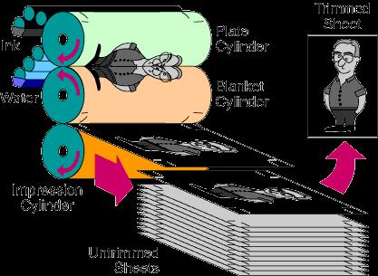
5 5 Solution: The Printing Process
6 6 The Photolithographic Process
7 7 CMOS Process/Transistors
8 Basic Process Flow Lightly Doped Wafer Grow Field Oxide Define Wells Grow Gate Oxide Deposit Poly Gate Etch Gates Implant Source/Drain Deposit Isolation Oxide and Contacts Deposit Metal 1 Deposit Isolation Oxide and Via 1 8 Deposit Metal 2

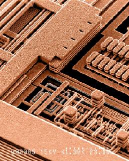
9 9 The Result
10 1 A Process Primer 2 Layout and DRC 3 Standard Cell Layout 4 Layout Planning Layout and Design Rules 10

11 Living in a 3D world 11 Courtesy: Arizona State University


12 Your Job Create cells that look like this: So the fab can transform it into this: 12
13 13 How do we layout a transistor?
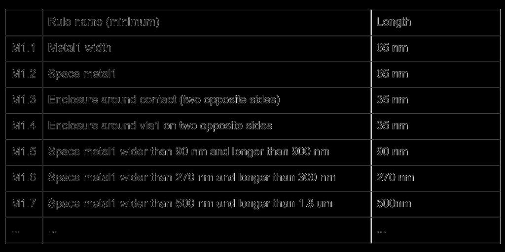
14 The Design Rule Manual Design Rules (also known as DRCs), are the interface between the designer and process engineer. The Design Rule Manual (DRM) provides guidelines for constructing process masks. These are generally categorized as: Intra-layer rules: minimum widths, spacing, area, etc., only relating to a single layer. Inter-layer rules: minimum enclosures, extensions, overlaps, etc., between two layers. Special rules: non geometric rules, such as antenna rules, density, distance to welltap, etc.
15 Common colors for layers Layer Layer Color Color Color Representation Representation,n) Well Well (p,n) (p,n) Yellow Yellow Yellow Area Active (n+,p+) Active Area Area (n+,p+) (n+,p+) Green (p+,n+) Select Select (p+,n+) (p+,n+) Green Green Green Green Green Transistor 1 conpolysilicon Polysilicon Red Red Red Metal1 Metal1 Blue Blue Blue 3 2 Metal2 Metal2 Magenta Magenta Magenta t To Contact Poly Contact To Poly To Poly Black Black Black t To Contact Diffusion Contact To Diffusion To Diffusion Black Black Black 5 Via Via Black Black Black 15


16 Design Rules Example 16 Source: FreePDK 45nm

17 Multi-finger Devices We can create wider or longer transistors using fingers: 17


18 Latchup The multiple n-type and p-type regions in the CMOS process create parasitic BJT transistors. Unintentional Thyristors can turn on and short V DD and G ND. This requires power down at the least, and sometimes causes chip destruction. 18 To eliminate some latchup, distribute well/substrate contacts across the chip.
19 Bulk Contacts To ensure a constant body voltage across large areas, Bulk Contacts or Taps have to be added frequently. N-well P-select P-sub N-select V DD V SS N-select pmos P-select nmos 19
20 1 A Process Primer 2 Layout and DRC 3 Standard Cell Layout 4 Layout Planning Standard Cell Layout 20


21 How to place millions of gates on a chip Reminder: ASIC design with Standard Cells Standard cells are like Legos They must meet certain design standards to be used together. Courtesy: Mantra VLSI 21
22 Standard Cell Properties Size: All cells have the same specified height, which is a multiple of track size. VDD and GND rails with specified width. N-well, p-active, n-active with specified width. Width is a multiple of the cell SITE minimum unit. Use fingers to implement wide transistors. Cell origin is set at (0,0) Routing: Only Metal 1 and Poly are used for routing. Pins are defined in Metal 1 on cross point of Metal 2 tracks for easy access. Half DRC pitch on sides to eliminate spacing violation. 22
23 How to layout a standard cell Good layout: dense and reliable Meets the manufacturing design rules (DRC) Matches the circuit being built (LVS) VSS IN VDD OUT Good or Bad? 23
24 Good Layout/Bad Layout! VSS IN VDD The previous layout was bad. The proper way to layout an inverter: VDD OUT Power Rails Feed through Schematic Poly length short and comes to M1 soon IN OUT 24 A substrate tap & well tap per cell is not necessary for every logic cell VSS
25 VDD IN VSS Fitting in Large Devices What if you had to layout an inverter with wide devices? You could do this VDD OUT 25 However, by doing so you are creating a layout that: Has long poly routes (high resistance) Has long source drain metal pickups (high resistance) Has an aspect ratio that is difficult to make work with other cells Has more periphery component of diffusion cap then it needs to Instead leg or fold transistors Small devices in parallel = same drive strength as one large device IN VSS OUT

26 Only use a single metal layer This can be very hard in a complex cell 26
27 Routing Grids Cell pins (except VDD/GND abutment pins) must be placed on the intersections of the vertical and horizontal routing grids. The routing grids are where the over-the-cell metal routing will be routed. Grids should usually be via-on-via to allow easy via placement in the cell. Line-on-via Min spacing, can t fit another via here Via-on-via Min spacing 27
28 Another short point about Standard Cells Standard Cells are a black-box abstraction for digital design. Therefore, we need to provide abstract views of our finalized gate: Behavioral model (Verilog) for logic simulation. Layout abstract for place and route (i.e., only essential information, such as cell size and pin locations) Timing and power characterizations, such as propagation delay, output transitions, input capacitance, static and dynamic power. Other views used by various EDA tools. We will learn how to extract layout abstracts and timing/power characterizations in the lab. 28
29 1 A Process Primer 2 Layout and DRC 3 Standard Cell Layout 4 Layout Planning Basic Layout Planning 29
30 Basic Layout Planning Okay, time to layout our new standard cell. Where do we start? Let s start with the obvious: Choose global directions for routing layers. Adjacent levels should route perpendicular Example: m2 horizontal, m1 vertical Position power lines first in top layer of metal Cluster together NMOS with NMOS and PMOS with PMOS And a bit less trivial: Arrange transistors so that common sources/drains can be shared Arrange transistors so that common gates line up Limit lengths of diffusion and poly routing use metal instead

31 An Example Step 1 Choose global directions for routing layers Position power lines in top layer of metal

32 An Example Step 2 Cluster together NMOS with NMOS and PMOS with PMOS Generally keep gate orientation the same

33 An Example Step 3 Arrange transistors so that common sources/drains can be shared Give precedence to shared signals over shared vdd/ground Arrange transistors so that common gates line up


34 An Example Step 4 Connect everything up and convert to layout

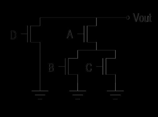
 So how do we find the better one?")
35 How do we choose the order of the signals? Let s take for example the function We could implement this in several ways. X = C (A + B) So how do we find the better one? 35 credit: NC State
36 The consistent Euler Path algorithm A B j C V out PUN V out = C (A + B) C C i V out i V DD A B A B B j GND A PDN 36 C Let s choose the path A B C
 C i A B 37 A B")
37 The consistent Euler Path algorithm A B j C X = C (A + B) C i A B 37 A B C

38 Another Example A B + C + D 38


39 39 Now find the consistent Euler paths


40 Plan the standard cell layout The Euler path we found was DACB: 40


41 ght of cell determined by metal width and spacing ease Final fingers Layout parameter in p-cells to eliminate contacts on side of the cell In older technologies, this allowed some savings of area as illustrated here. In newer technologies (45nm), poly pitch cannot be reduced, even if there are no contacts. 41 avis NC State University Slide 19 ECE 546 Fall 2012
42 Further Reading Arizona State University EEE 525 (Lawrence Clark) NC State University 42
Digital Integrated CircuitDesign
 Digital Integrated CircuitDesign Lecture 8 Design Rules Adib Abrishamifar EE Department IUST Contents Design Rules CMOS Process Layers Intra-Layer Design Rules Via s and Contacts Select Layer Example Cell
ESE 570 Cadence Lab Assignment 2: Introduction to Spectre, Manual Layout Drawing and Post Layout Simulation (PLS)
") ESE 570 Cadence Lab Assignment 2: Introduction to Spectre, Manual Layout Drawing and Post Layout Simulation (PLS) Objective Part A: To become acquainted with Spectre (or HSpice) by simulating an inverter,
ESE 570 Cadence Lab Assignment 2: Introduction to Spectre, Manual Layout Drawing and Post Layout Simulation (PLS) Objective Part A: To become acquainted with Spectre (or HSpice) by simulating an inverter,
CMOS Process Flow. Layout CAD Tools
 CMOS Process Flow See supplementary power point file for animated CMOS process flow (see class ece410 website and/or* http://www.multimedia.vt.edu/ee5545/): This file should be viewed as a slide show It
Lay ay ut Design g R ules
 HPTER 5: Layout esign Rules Introduction ny circuit physical mask layout must conform to a set of geometric constraints or rules called as Layout esign rules before it can be manufactured using particular
Composite Layout CS/EE N-type from the top. N-type Transistor. Diffusion Mask. Polysilicon Mask
 Composite Layout CS/EE 6710 Introduction to Layout Inverter Layout Example Layout Design Rules Drawing the mask layers that will be used by the fabrication folks to make the devices Very different from
UNIVERSITY OF CALIFORNIA College of Engineering Department of Electrical Engineering and Computer Sciences Lab #2: Layout and Simulation
 UNIVERSITY OF CALIFORNIA College of Engineering Department of Electrical Engineering and Computer Sciences Lab #2: Layout and Simulation NTU IC541CA 1 Assumed Knowledge This lab assumes use of the Electric
Design rule illustrations for the AMI C5N process can be found at:
 Cadence Tutorial B: Layout, DRC, Extraction, and LVS Created for the MSU VLSI program by Professor A. Mason and the AMSaC lab group. Revised by C Young & Waqar A Qureshi -FS08 Document Contents Introduction
Digital Integrated Circuits (83-313) Lecture 7: SRAM. Semester B, Lecturer: Dr. Adam Teman Itamar Levi, Robert Giterman.
 Lecture 7: SRAM. Semester B, Lecturer: Dr. Adam Teman Itamar Levi, Robert Giterman.") Digital Integrated Circuits (83-313) Lecture 7: SRAM Semester B, 2016-17 Lecturer: Dr. Adam Teman TAs: Itamar Levi, Robert Giterman 16 May 2017 Disclaimer: This course was prepared, in its entirety, by
Digital Integrated Circuits (83-313) Lecture 7: SRAM Semester B, 2016-17 Lecturer: Dr. Adam Teman TAs: Itamar Levi, Robert Giterman 16 May 2017 Disclaimer: This course was prepared, in its entirety, by
FABRICATION OF CMOS INTEGRATED CIRCUITS. Dr. Mohammed M. Farag
 FABRICATION OF CMOS INTEGRATED CIRCUITS Dr. Mohammed M. Farag Outline Overview of CMOS Fabrication Processes The CMOS Fabrication Process Flow Design Rules EE 432 VLSI Modeling and Design 2 CMOS Fabrication
VLSI Lab Tutorial 3. Virtuoso Layout Editing Introduction
 VLSI Lab Tutorial 3 Virtuoso Layout Editing Introduction 1.0 Introduction The purpose of this lab tutorial is to guide you through the design process in creating a custom IC layout for your CMOS inverter
TUTORIAL II ECE 555 / 755 Updated on September 11 th 2006 CADENCE LAYOUT AND PARASITIC EXTRACTION
 TUTORIAL II ECE 555 / 755 Updated on September 11 th 2006 CADENCE LAYOUT AND PARASITIC EXTRACTION After finishing a schematic of your design (Tutorial-I), the next step is creating masks which are for
Spiral 2-8. Cell Layout
 2-8.1 Spiral 2-8 Cell Layout 2-8.2 Learning Outcomes I understand how a digital circuit is composed of layers of materials forming transistors and wires I understand how each layer is expressed as geometric
Cadence Virtuoso Schematic Design and Circuit Simulation Tutorial
 Cadence Virtuoso Schematic Design and Circuit Simulation Tutorial Introduction This tutorial is an introduction to schematic capture and circuit simulation for ENGN1600 using Cadence Virtuoso. These courses
Process technology and introduction to physical
 Neuromorphic Engineering II Lab 3, Spring 2014 1 Lab 3 March 10, 2014 Process technology and introduction to physical layout Today you will start to learn to use the Virtuoso layout editor XL which is
Cadence Tutorial 2: Layout, DRC/LVS and Circuit Simulation with Extracted Parasitics
 Cadence Tutorial 2: Layout, DRC/LVS and Circuit Simulation with Extracted Parasitics Introduction This tutorial describes how to generate a mask layout in the Cadence Virtuoso Layout Editor. Use of DIVA
EE 330 Laboratory 3 Layout, DRC, and LVS Fall 2015
 EE 330 Laboratory 3 Layout, DRC, and LVS Fall 2015 Contents Objective:... 2 Part 1 Creating a layout... 2 1.1 Run DRC Early and Often... 2 1.2 Create N active and connect the transistors... 3 1.3 Vias...
Circuits. L3: Fabrication and Layout -1 ( ) B. Mazhari Dept. of EE, IIT Kanpur. B. Mazhari, IITK. G-Number
 B. Mazhari Dept. of EE, IIT Kanpur. B. Mazhari, IITK. G-Number") EE60: CMOS Analog Circuits L: Fabrication and Layout - (8.8.0) B. Mazhari Dept. of EE, IIT Kanpur Suppose we have a Silicon wafer which is P-type and we wish to create a region within it which is N-type
EE60: CMOS Analog Circuits L: Fabrication and Layout - (8.8.0) B. Mazhari Dept. of EE, IIT Kanpur Suppose we have a Silicon wafer which is P-type and we wish to create a region within it which is N-type
EE 330 Laboratory 3 Layout, DRC, and LVS
 EE 330 Laboratory 3 Layout, DRC, and LVS Spring 2018 Contents Objective:... 2 Part 1 creating a layout... 2 1.1 Run DRC... 2 1.2 Stick Diagram to Physical Layer... 3 1.3 Bulk Connections... 3 1.4 Pins...
ECE471/571 Energy Efficient VLSI Design Project 2 Cadence Setup and Creation of an Inverter Due Date 11:30 am on Friday, February 2 nd, 2018
 ECE471/571 Energy Efficient VLSI Design Project 2 Cadence Setup and Creation of an Inverter Due Date 11:30 am on Friday, February 2 nd, 2018 Introduction This project will first walk you through the setup
Lab 2. Standard Cell layout.
 Lab 2. Standard Cell layout. The purpose of this lab is to demonstrate CMOS-standard cell design. Use the lab instructions and the cadence manual (http://www.es.lth.se/ugradcourses/cadsys/cadence.html)
3. Implementing Logic in CMOS
 3. Implementing Logic in CMOS 3. Implementing Logic in CMOS Jacob Abraham Department of Electrical and Computer Engineering The University of Texas at Austin VLSI Design Fall 27 September, 27 ECE Department,
On the Design of Ultra-High Density 14nm Finfet based Transistor-Level Monolithic 3D ICs
 2016 IEEE Computer Society Annual Symposium on VLSI On the Design of Ultra-High Density 14nm Finfet based Transistor-Level Monolithic 3D ICs Jiajun Shi 1,2, Deepak Nayak 1,Motoi Ichihashi 1, Srinivasa
Lab. Course Goals. Topics. What is VLSI design? What is an integrated circuit? VLSI Design Cycle. VLSI Design Automation
 Course Goals Lab Understand key components in VLSI designs Become familiar with design tools (Cadence) Understand design flows Understand behavioral, structural, and physical specifications Be able to
Integrated Circuits & Systems
 Federal University of Santa Catarina Center for Technology Computer Science & Electronics Engineering Integrated Circuits & Systems INE 5442 Lecture 23-1 guntzel@inf.ufsc.br Semiconductor Memory Classification
Virtuoso Layout Editor
 This tutorial will cover the basic steps involved in using the Cadence layout editor called Virtuoso, extracting layout, and running simulation on the layout. The inverter layout is used as an example
TABLE OF CONTENTS 1.0 PURPOSE INTRODUCTION ESD CHECKS THROUGHOUT IC DESIGN FLOW... 2
 TABLE OF CONTENTS 1.0 PURPOSE... 1 2.0 INTRODUCTION... 1 3.0 ESD CHECKS THROUGHOUT IC DESIGN FLOW... 2 3.1 PRODUCT DEFINITION PHASE... 3 3.2 CHIP ARCHITECTURE PHASE... 4 3.3 MODULE AND FULL IC DESIGN PHASE...
Single-Strip Static CMOS Layout
 EE244: Design Technology for Integrated Circuits and Systems Outline Lecture 6.2 Regular Module Structures CMOS Synthetic Libraries Weinberger Arrays Gate Matrix Programmable Logic Array (PLA) Storage
Lecture 4a. CMOS Fabrication, Layout and Simulation. R. Saleh Dept. of ECE University of British Columbia
 Lecture 4a CMOS Fabrication, Layout and Simulation R. Saleh Dept. of ECE University of British Columbia res@ece.ubc.ca 1 Fabrication Fabrication is the process used to create devices and wires. Transistors
EE 330 Spring 2018 Laboratory 2: Basic Boolean Circuits
 EE 330 Spring 2018 Laboratory 2: Basic Boolean Circuits Contents Objective:... 2 Part 1: Introduction... 2 Part 2 Simulation of a CMOS Inverter... 3 Part 2.1 Attaching technology information... 3 Part
ESE570 Spring University of Pennsylvania Department of Electrical and System Engineering Digital Integrated Cicruits AND VLSI Fundamentals
 University of Pennsylvania Department of Electrical and System Engineering Digital Integrated Cicruits AND VLSI Fundamentals ESE570, Spring 2019 HW5: Delay and Layout Sunday, February 17th Due: Friday,
Cell Libraries and Design Hierarchy. Instructor S. Demlow ECE 410 February 1, 2012
 Cell Libraries and Design Hierarchy Instructor S. Demlow ECE 410 February 1, 2012 Stick Diagrams Simplified NAND Layout Simplified NOR Layout Metal supply rails blue n and p Active green Poly gates red
Introduction to ICs and Transistor Fundamentals
 Introduction to ICs and Transistor Fundamentals A Brief History 1958: First integrated circuit Flip-flop using two transistors Built by Jack Kilby at Texas Instruments 2003 Intel Pentium 4 mprocessor (55
Latch-up Verification / Rule Checking Throughout Circuit Design Flow
 Latch-up Verification / Rule Checking Throughout Circuit Design Flow Michael Khazhinsky ESD and Latch-up Design Silicon Labs April 2016 Motivation The verification of latch-up protection networks in modern
Logging in, starting a shell tool, and starting the Cadence Tool Suite
 EEE 4134 VLSI I Laboratory Lab 0 (Introductory Lab) Logging into Cadence Server, Tool Setup, Cell Library Creation, Introduction to Custom IC Design flow Objectives: To login, start a shell tool and start
EE115C Digital Electronic Circuits. Tutorial 4: Schematic-driven Layout (Virtuoso XL)
") EE115C Digital Electronic Circuits Tutorial 4: Schematic-driven Layout (Virtuoso XL) This tutorial will demonstrate schematic-driven layout on the example of a 2-input NAND gate. Simple Layout (that won
EE115C Digital Electronic Circuits Tutorial 4: Schematic-driven Layout (Virtuoso XL) This tutorial will demonstrate schematic-driven layout on the example of a 2-input NAND gate. Simple Layout (that won
FABRICATION TECHNOLOGIES
 FABRICATION TECHNOLOGIES DSP Processor Design Approaches Full custom Standard cell** higher performance lower energy (power) lower per-part cost Gate array* FPGA* Programmable DSP Programmable general
Computer-Based Project on VLSI Design Co 3/7
 Computer-Based Project on VLSI Design Co 3/7 IC Layout and Symbolic Representation This pamphlet introduces the topic of IC layout in integrated circuit design and discusses the role of Design Rules and
Magic Technology Manual #1: NMOS
 Magic Technology Manual #1: NMOS John Ousterhout Computer Science Division Electrical Engineering and Computer Sciences University of California Berkeley, CA 970 (Warning: Process details often change.
CPE/EE 427, CPE 527, VLSI Design I: Tutorial #1, Full Custom VLSI (inverter layout)
") CPE/EE 427, CPE 527, VLSI Design I: Tutorial #1, Full Custom VLSI (inverter layout) Joel Wilder, Aleksandar Milenkovic, ECE Dept., The University of Alabama in Huntsville Adapted from Virginia Tech, Dept.
CPE/EE 427, CPE 527, VLSI Design I: Tutorial #1, Full Custom VLSI (inverter layout) Joel Wilder, Aleksandar Milenkovic, ECE Dept., The University of Alabama in Huntsville Adapted from Virginia Tech, Dept.
Methodology on Extracting Compact Layout Rules for Latchup Prevention in Deep-Submicron Bulk CMOS Technology
 IEEE TRANSACTIONS ON SEMICONDUCTOR MANUFACTURING, VOL. 16, NO. 2, MAY 2003 319 Methodology on Extracting Compact Layout Rules for Latchup Prevention in Deep-Submicron Bulk CMOS Technology Ming-Dou Ker,
A Framework for Systematic Evaluation and Exploration of Design Rules
 A Framework for Systematic Evaluation and Exploration of Design Rules Rani S. Ghaida* and Prof. Puneet Gupta EE Dept., University of California, Los Angeles (rani@ee.ucla.edu), (puneet@ee.ucla.edu) Work
CMOS INVERTER LAYOUT TUTORIAL
 PRINCESS SUMAYA UNIVERSITY FOR TECHNOLOGY CMOS INVERTER LAYOUT TUTORIAL We will start the inverter by drawing a PMOS. The first step is to draw a poly layer. Click on draw a rectangle and choose the poly
UNIVERSITY OF WATERLOO
 UNIVERSITY OF WATERLOO UW ASIC DESIGN TEAM: Cadence Tutorial Description: Part I: Layout & DRC of a CMOS inverter. Part II: Extraction & LVS of a CMOS inverter. Part III: Post-Layout Simulation. The Cadence
Memory Arrays. Array Architecture. Chapter 16 Memory Circuits and Chapter 12 Array Subsystems from CMOS VLSI Design by Weste and Harris, 4 th Edition
 Chapter 6 Memory Circuits and Chapter rray Subsystems from CMOS VLSI Design by Weste and Harris, th Edition E E 80 Introduction to nalog and Digital VLSI Paul M. Furth New Mexico State University Static
SRAM Memory Layout Design in 180nm Technology
 SRAM Memory Layout Design in 180nm Technology Praveen K N M.Tech in VLSI Design & Embedded Systems JSS Academy of Technical Education, Bengaluru, India B. G. Shivaleelavathi Professor, H.O. D ECE Department,
Digital VLSI Design. Lecture 9: Routing
 Digital VLSI Design Lecture 9: Routing Semester A, 018-19 Lecturer: Dr. Adam Teman January 5, 019 Disclaimer: This course was prepared, in its entirety, by Adam Teman. Many materials were copied from sources
ECE471/571 Energy Ecient VLSI Design
 ECE471/571 Energy Ecient VLSI Design Project 2 Cadence Setup and Creation of an Inverter Due Date 11:30pm on Friday, January 30 th 2015 Introduction This project will rst walk you through the setup for
Power IC 용 ESD 보호기술. 구용서 ( Yong-Seo Koo ) Electronic Engineering Dankook University, Korea
 Electronic Engineering Dankook University, Korea") Power IC 용 ESD 보호기술 구용서 ( Yong-Seo Koo ) Electronic Engineering Dankook University, Korea yskoo@dankook.ac.kr 031-8005-3625 Outline Introduction Basic Concept of ESD Protection Circuit ESD Technology Issue
Power IC 용 ESD 보호기술 구용서 ( Yong-Seo Koo ) Electronic Engineering Dankook University, Korea yskoo@dankook.ac.kr 031-8005-3625 Outline Introduction Basic Concept of ESD Protection Circuit ESD Technology Issue
UNIT IV CMOS TESTING
 UNIT IV CMOS TESTING 1. Mention the levels at which testing of a chip can be done? At the wafer level At the packaged-chip level At the board level At the system level In the field 2. What is meant by
Memory Design I. Array-Structured Memory Architecture. Professor Chris H. Kim. Dept. of ECE.
 Memory Design I Professor Chris H. Kim University of Minnesota Dept. of ECE chriskim@ece.umn.edu Array-Structured Memory Architecture 2 1 Semiconductor Memory Classification Read-Write Wi Memory Non-Volatile
Art of Layout Euler s path and stick diagram. Kunal Ghosh
 Art of Layout Euler s path and stick diagram Kunal Ghosh I wrote about Euler s path and stick diagram in two different blogs, but now is the time to show you how are they connected. It s simple and, seems,
Introduction to Layout design
 Introduction to Layout design Note: some figures are taken from Ref. B. Razavi, Design of Analog CMOS integrated circuits, Mc Graw-Hill, 001, and MOSIS web site: http://www.mosis.org/ 1 Introduction to
VBIT COURSE MATERIAL VLSI DESIGN
 UNIT II VLSI CIRCUIT DESIGN PROCESSES: VLSI Design Flow, MOS Layers, Stick Diagrams, Design Rules and Layout, 2μm CMOS Design rules for wires, Contacts and Transistors Layout Diagrams for NMOS and CMOS
Taming the Challenges of 20nm Custom/Analog Design
 Taming the Challenges of 20nm Custom/Analog Design Custom and analog designers will lay the foundation for 20nm IC design. However, they face many challenges that arise from manufacturing complexity. The
Improved Circuit Reliability/Robustness. Carey Robertson Product Marketing Director Mentor Graphics Corporation
 Improved Circuit Reliability/Robustness Carey Robertson Product Marketing Director Mentor Graphics Corporation Reliability Requirements are Growing in all Market Segments Transportation Mobile / Wireless
VLSI Test Technology and Reliability (ET4076)
") VLSI Test Technology and Reliability (ET4076) Lecture 8(2) I DDQ Current Testing (Chapter 13) Said Hamdioui Computer Engineering Lab Delft University of Technology 2009-2010 1 Learning aims Describe the
VLSI Test Technology and Reliability (ET4076) Lecture 8(2) I DDQ Current Testing (Chapter 13) Said Hamdioui Computer Engineering Lab Delft University of Technology 2009-2010 1 Learning aims Describe the
Very Large Scale Integration (VLSI)
") Very Large Scale Integration (VLSI) Lecture 8 Dr. Ahmed H. Madian ah_madian@hotmail.com Content Array Subsystems Introduction General memory array architecture SRAM (6-T cell) CAM Read only memory Introduction
Very Large Scale Integration (VLSI) Lecture 8 Dr. Ahmed H. Madian ah_madian@hotmail.com Content Array Subsystems Introduction General memory array architecture SRAM (6-T cell) CAM Read only memory Introduction
10. Interconnects in CMOS Technology
 10. Interconnects in CMOS Technology 1 10. Interconnects in CMOS Technology Jacob Abraham Department of Electrical and Computer Engineering The University of Texas at Austin VLSI Design Fall 2017 October
ECE 5745 Complex Digital ASIC Design Topic 7: Packaging, Power Distribution, Clocking, and I/O
 ECE 5745 Complex Digital ASIC Design Topic 7: Packaging, Power Distribution, Clocking, and I/O Christopher Batten School of Electrical and Computer Engineering Cornell University http://www.csl.cornell.edu/courses/ece5745
Texas Instruments TMX320TCI6488ZUNV Baseband Processor System on a Chip
 Texas Instruments TMX320TCI6488ZUNV Baseband Processor System on a Chip Structural Analysis For comments, questions, or more information about this report, or for any additional technical needs concerning
Numonyx JSPCM128A00B85ES 128 Mbit Phase Change Memory 90 nm BiCMOS PCM Process
 Numonyx JSPCM128A00B85ES 90 nm BiCMOS PCM Process Structural Analysis For comments, questions, or more information about this report, or for any additional technical needs concerning semiconductor technology,
A Review Paper on Reconfigurable Techniques to Improve Critical Parameters of SRAM
 IJSRD - International Journal for Scientific Research & Development Vol. 4, Issue 09, 2016 ISSN (online): 2321-0613 A Review Paper on Reconfigurable Techniques to Improve Critical Parameters of SRAM Yogit
Introduction 1. GENERAL TRENDS. 1. The technology scale down DEEP SUBMICRON CMOS DESIGN
 1 Introduction The evolution of integrated circuit (IC) fabrication techniques is a unique fact in the history of modern industry. The improvements in terms of speed, density and cost have kept constant
Full Custom Layout Optimization Using Minimum distance rule, Jogs and Depletion sharing
 Full Custom Layout Optimization Using Minimum distance rule, Jogs and Depletion sharing Umadevi.S #1, Vigneswaran.T #2 # Assistant Professor [Sr], School of Electronics Engineering, VIT University, Vandalur-
Lecture 11: MOS Memory
 Lecture 11: MOS Memory MAH, AEN EE271 Lecture 11 1 Memory Reading W&E 8.3.1-8.3.2 - Memory Design Introduction Memories are one of the most useful VLSI building blocks. One reason for their utility is
IMPLEMENTATION OF LOW POWER AREA EFFICIENT ALU WITH LOW POWER FULL ADDER USING MICROWIND DSCH3
 IMPLEMENTATION OF LOW POWER AREA EFFICIENT ALU WITH LOW POWER FULL ADDER USING MICROWIND DSCH3 Ritafaria D 1, Thallapalli Saibaba 2 Assistant Professor, CJITS, Janagoan, T.S, India Abstract In this paper
NVIDIA Tegra T20-H-A2 Application Processor TSMC 40 nm Low Power CMOS Process
 NVIDIA Tegra T20-H-A2 Application Processor TSMC 40 nm Low Power CMOS Process Structural Analysis 3685 Richmond Road, Suite 500, Ottawa, ON K2H 5B7 Canada Tel: 613-829-0414 www.chipworks.com Structural
Micro transductors 08
 Micro transductors 8 CMOS Basics Dr.-Ing. Frank Sill Department of Electrical Engineering, Federal University of Minas Gerais, Av. Antônio Carlos 6627, CEP: 327-, Belo Horizonte (MG), Brazil franksill@ufmg.br
Lecture Content. 1 Adam Teman, 2018
 Lecture Content 1 Adam Teman, 2018 Digital VLSI Design Lecture 6: Moving to the Physical Domain Semester A, 2018-19 Lecturer: Dr. Adam Teman December 24, 2018 Disclaimer: This course was prepared, in its
ENEE 359a Digital VLSI Design
 SLIDE 1 ENEE 359a Digital VLSI Design Course : Transistors to Systems Prof. blj@eng.umd.edu Credit where credit is due: Slides contain original artwork ( Jacob 2004) as well as material taken liberally
Electromagnetic Compatibility ( EMC )
") Electromagnetic Compatibility ( EMC ) ESD Strategies in IC and System Design 8-1 Agenda ESD Design in IC Level ( ) Design Guide Lines CMOS Design Process Level Method Circuit Level Method Whole Chip Design
Electromagnetic Compatibility ( EMC ) ESD Strategies in IC and System Design 8-1 Agenda ESD Design in IC Level ( ) Design Guide Lines CMOS Design Process Level Method Circuit Level Method Whole Chip Design
CS310 Embedded Computer Systems. Maeng
 1 INTRODUCTION (PART II) Maeng Three key embedded system technologies 2 Technology A manner of accomplishing a task, especially using technical processes, methods, or knowledge Three key technologies for
+1 (479)
") Memory Courtesy of Dr. Daehyun Lim@WSU, Dr. Harris@HMC, Dr. Shmuel Wimer@BIU and Dr. Choi@PSU http://csce.uark.edu +1 (479) 575-6043 yrpeng@uark.edu Memory Arrays Memory Arrays Random Access Memory Serial
Memory Courtesy of Dr. Daehyun Lim@WSU, Dr. Harris@HMC, Dr. Shmuel Wimer@BIU and Dr. Choi@PSU http://csce.uark.edu +1 (479) 575-6043 yrpeng@uark.edu Memory Arrays Memory Arrays Random Access Memory Serial
CMOS Design Lab Manual
 CMOS Design Lab Manual Developed By University Program Team CoreEl Technologies (I) Pvt. Ltd. 1 Objective Objective of this lab is to learn the Mentor Graphics HEP2 tools as well learn the flow of the
Very Large Scale Integration (VLSI)
") Very Large Scale Integration (VLSI) Lecture 6 Dr. Ahmed H. Madian Ah_madian@hotmail.com Dr. Ahmed H. Madian-VLSI 1 Contents FPGA Technology Programmable logic Cell (PLC) Mux-based cells Look up table PLA
Very Large Scale Integration (VLSI) Lecture 6 Dr. Ahmed H. Madian Ah_madian@hotmail.com Dr. Ahmed H. Madian-VLSI 1 Contents FPGA Technology Programmable logic Cell (PLC) Mux-based cells Look up table PLA
An overview of standard cell based digital VLSI design
 An overview of standard cell based digital VLSI design Implementation of the first generation AsAP processor Zhiyi Yu and Tinoosh Mohsenin VCL Laboratory UC Davis Outline Overview of standard cellbased
QUESTION BANK DEPARTMENT OF ECE
 QUESTION BANK DEPARTMENT OF ECE YEAR: III SEM: VI SUBJECTCODE:EC2354 SUBJECT NAME:VLSI DESIGN Prepared by V.GUNASUNDARI/AP 1.List the advantages of SOI CMOS process Denser transistor structures are possible.
Physical Implementation
 CS250 VLSI Systems Design Fall 2009 John Wawrzynek, Krste Asanovic, with John Lazzaro Physical Implementation Outline Standard cell back-end place and route tools make layout mostly automatic. However,
Problem Formulation. Specialized algorithms are required for clock (and power nets) due to strict specifications for routing such nets.
 due to strict specifications for routing such nets.") Clock Routing Problem Formulation Specialized algorithms are required for clock (and power nets) due to strict specifications for routing such nets. Better to develop specialized routers for these nets.
Clock Routing Problem Formulation Specialized algorithms are required for clock (and power nets) due to strict specifications for routing such nets. Better to develop specialized routers for these nets.
CHAPTER 3 SIMULATION TOOLS AND
 CHAPTER 3 SIMULATION TOOLS AND Simulation tools used in this simulation project come mainly from Integrated Systems Engineering (ISE) and SYNOPSYS and are employed in different areas of study in the simulation
Samsung K9GAG08U0M-PCB0 16 Gbit Multi-Level Cell (MLC) 51 nm Process Technology NAND Flash Memory
 51 nm Process Technology NAND Flash Memory") Samsung K9GAG08U0M-PCB0 16 Gbit Multi-Level Cell (MLC) 51 nm Process Technology NAND Flash Memory Structural Analysis with Additional Layout Feature Analysis For comments, questions, or more information
Samsung K9GAG08U0M-PCB0 16 Gbit Multi-Level Cell (MLC) 51 nm Process Technology NAND Flash Memory Structural Analysis with Additional Layout Feature Analysis For comments, questions, or more information
Enhancing and Using an Automatic Design System for Creating FPGAs. Aaron Charles Egier
 Enhancing and Using an Automatic Design System for Creating FPGAs by Aaron Charles Egier A thesis submitted in conformity with the requirements for the degree of Master of Applied Science Graduate Department
Professor Muller Fall 2016 Sameet Ramakrishnan Eric Chang Adapted from prior EE140 and EE141 labs. EE 140/240A Lab 0 Full IC Design Flow
 Professor Muller Fall 2016 Sameet Ramakrishnan Eric Chang Adapted from prior EE140 and EE141 labs EE 140/240A Lab 0 Full IC Design Flow In this lab, you will walk through the full process an analog designer
Virtuoso Schematic Composer
 is a schematic design tool from Cadence. In this tutorial you will learn how to put electrical components, make wire connections, insert pins and check for connection error. Start Cadence Custom IC Design
More information can be found in the Cadence manuals Virtuoso Layout Editor User Guide and Cadence Hierarchy Editor User Guide.
 Chapter 6 Building with Layout This chapter consists of two parts. The first describes the generation of layout views and the second deals with the various tools used for verifying the layout, both physical
Prepared by Dr. Ulkuhan Guler GT-Bionics Lab Georgia Institute of Technology
 Prepared by Dr. Ulkuhan Guler GT-Bionics Lab Georgia Institute of Technology OUTLINE Introduction Mapping for Schematic and Layout Connectivity Generate Layout from Schematic Connectivity Some Useful Features
Integrated circuits and fabrication
 Integrated circuits and fabrication Motivation So far we have discussed about the various devices that are the heartbeat of core electronics. This modules aims at giving an overview of how these solid
ECE410 Design Project Spring 2013 Design and Characterization of a CMOS 8-bit pipelined Microprocessor Data Path
 ECE410 Design Project Spring 2013 Design and Characterization of a CMOS 8-bit pipelined Microprocessor Data Path Project Summary This project involves the schematic and layout design of an 8-bit microprocessor
ASIC Physical Design Top-Level Chip Layout
 ASIC Physical Design Top-Level Chip Layout References: M. Smith, Application Specific Integrated Circuits, Chap. 16 Cadence Virtuoso User Manual Top-level IC design process Typically done before individual
On-Chip Variation (OCV) Kunal Ghosh
 Kunal Ghosh") On-Chip Variation (OCV) Kunal Ghosh Ever thought what s an interviewer s favorite questions to rip you off all my previous ebooks. And On-Chip Variation (OCV) is one of them, specifically for Static Timing
On-Chip Variation (OCV) Kunal Ghosh Ever thought what s an interviewer s favorite questions to rip you off all my previous ebooks. And On-Chip Variation (OCV) is one of them, specifically for Static Timing
Cadence Tutorial. Introduction to Cadence 0.18um, Implementation and Simulation of an inverter. A. Moradi, A. Miled et M. Sawan
 Cadence Tutorial Introduction to Cadence 0.18um, Implementation and Simulation of an inverter A. Moradi, A. Miled et M. Sawan Section 1: Introduction to Cadence You will see how to create a new library
ENEE 359a Digital VLSI Design
 SLIDE 1 ENEE 359a Digital VLSI Design CMOS Memories and Systems: Part II, Prof. blj@eng.umd.edu Credit where credit is due: Slides contain original artwork ( Jacob 1999 2004, Wang 2003/4) as well as material
Brief Introduction of Cell-based Design. Ching-Da Chan CIC/DSD
 Brief Introduction of Cell-based Design Ching-Da Chan CIC/DSD 1 Design Abstraction Levels SYSTEM MODULE + GATE CIRCUIT S n+ G DEVICE n+ D 2 Full Custom V.S Cell based Design Full custom design Better patent
EE 140/240A - Full IC Design Flow Tutorial
 Original document by Filip Maksimovic & Mike Lorek, Spring 2015, derived from earlier EE141 lab manuals Revisions for IC6 by David Burnett & Thaibao Phan, Spring 2016 Revisions made by Nandish Mehta to
Cadence IC Design Manual
 Cadence IC Design Manual For EE5518 ZHENG Huan Qun Lin Long Yang Revised on May 2017 Department of Electrical & Computer Engineering National University of Singapore 1 P age Contents 1 INTRODUCTION...
0.35um design verifications
 0.35um design verifications Path end segment check (END) First check is the end segment check, This error is related to the routing metals when routing is done with a path. The finish of this path can
PAPER MOS-Bounded Diodes for On-Chip ESD Protection in Deep Submicron CMOS Process
 IEICE TRANS. ELECTRON., VOL.E88 C, NO.3 MARCH 2005 429 PAPER MOS-Bounded Diodes for On-Chip ESD Protection in Deep Submicron CMOS Process Ming-Dou KER a), Kun-Hsien LIN, and Che-Hao CHUANG, Nonmembers
Latch-Up. Parasitic Bipolar Transistors
 Latch-Up LATCH-UP CIRCUIT Latch-up is caused by an SCR (Silicon Controlled Rectifier) circuit. Fabrication of CMOS integrated circuits with bulk silicon processing creates a parasitic SCR structure. The
Memory Design I. Semiconductor Memory Classification. Read-Write Memories (RWM) Memory Scaling Trend. Memory Scaling Trend
 Memory Scaling Trend. Memory Scaling Trend") Array-Structured Memory Architecture Memory Design I Professor hris H. Kim University of Minnesota Dept. of EE chriskim@ece.umn.edu 2 Semiconductor Memory lassification Read-Write Memory Non-Volatile Read-Write
Array-Structured Memory Architecture Memory Design I Professor hris H. Kim University of Minnesota Dept. of EE chriskim@ece.umn.edu 2 Semiconductor Memory lassification Read-Write Memory Non-Volatile Read-Write
Amplifier Simulation Tutorial. Design Kit: Cadence 0.18μm CMOS PDK (gpdk180) (Cadence Version 6.1.5)
 (Cadence Version 6.1.5)") Amplifier Simulation Tutorial Design Kit: Cadence 0.18μm CMOS PDK (gpdk180) (Cadence Version 6.1.5) Yongsuk Choi, Marvin Onabajo This tutorial provides a quick introduction to the use of Cadence tools
Amplifier Simulation Tutorial Design Kit: Cadence 0.18μm CMOS PDK (gpdk180) (Cadence Version 6.1.5) Yongsuk Choi, Marvin Onabajo This tutorial provides a quick introduction to the use of Cadence tools