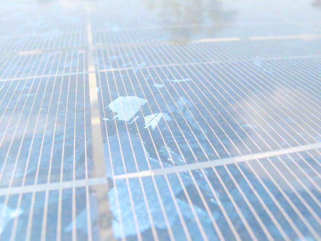
3D Surface Metrology on PV Solar Wafers
|
|
|
- Paula Cross
- 6 years ago
- Views:
Transcription

1 3D Surface Metrology on PV Solar Wafers Karl- Heinz Strass cybertechnologies USA 962 Terra Bella Ave San Jose CA P:
2 Introduction Solar photovoltaics is the fastest growing power-generation technology in the world, with an average growth rate of over 20 percent per year since Driven by advances in technology the conversion rate has steadily increased to well above 20 % in commercially available cells, while research labs have proven efficiencies of over 40%. The efficiency of a solar cells is the product of multiple parameters, one of which is reflectance efficiency, a significant portion of the (external) quantum efficiency, the percentage of photons converted to electric current. Surface topography, typically achieved by chemically texturing the wafer surface has a high degree of influence on the reflective properties of the wafer. Technology overview Traditionally, surface topography used to be measured with contacting stylus profilometers. However, due to the sensitivity of the surfaces, contacting method no longer meet the requirements of the industry. On the other hand, AFM technology, although it offers outstanding resolution, is not feasible due to the limited measurement area and scan speed. This lead to the advance of optical surface metrology systems, which can roughly be broken into two groups: Microscope based systems, with relatively high resolution but limited measurement size and scanning systems, where a point source is moved relatively to the sample surface and the surface variation is detected. The advantage of scanning systems lies within their capability to measure over large areas without impact on measurement resolution. They also provide much larger dynamic measurement ranges at high resolutions than microscope based systems. A major challenge for most optical systems is the measurement of the surface topography on samples coated with anti-reflective films. The films are designed to prevent the incident light from reflecting off the substrate, resulting in low levels of reflected light for the purpose of measuring the surface. cybertechnologies has developed a system that is optimized for these applications. cybertechnologies is a leading manufacturer of high-resolution 3D scanning surface metrology systems, with vertical resolution down to 3 nm and sample sizes of over 600 mm x 600 mm.
3 Objective A cybertechnologies cyberscan VANTAGE system with the small spot, ARC-optimized sensor is used to measure the surface of solar wafers. The surface parameters of interest are automatically determined. Measurement technology A laser beam is focused on the sample through an objective lens that moves up and down. The optical system is designed such that the maximum light intensity occurs when the sample surface lies within the focal plane of the objective. The reflected light is imaged through a pinhole onto a detector. As the objective moves closer or further away from the surface, the reflected light reaching the pinhole is defocused and the intensity decreases. The electronics collect a data point when the intensity of light imaged through the pinhole reaches a maximum. The sensor works on most any surface and is also widely used for measuring roughness and very small features on other engineered surfaces as well as on optically transparent or translucent films, like flux.

4 Measurement results A user- configurable screen layout shows all the pertinent information at one glance: - Measurement parameters selected, such as scan dimensions and lateral resolution - 3D raster screen, with false color controls - Selected 3D surface parameters - 2D line profile of user selected cross- section - 2D surface profile parameters - Abbott- Firestone curve and parametric results - Surface histogram with results and user defined thresholds


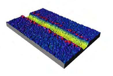
5 False color raster of scanned area on left and a 3D rendering of the surface below. The blue line indicates where the 2D line profile is extracted. The user can easily move the line up and down, or even change the angle of the virtual cut.
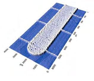
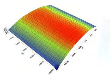
6 Advanced surface analysis Abbott- Firestone or bearing- ratio curve: Definition This analysis is useful to better understand the physical surface properties that the incident light interacts with as it more precisely describes the texture of a given surface. It essentially provides a fingerprint of the surface. The Abbott-Firestone Curve is determined mathematically by integrating the trace profile. With some mathematical modifications the concept can be adapted to a three- dimensional area. Image Source: Wikipedia, free encyclopedia File:Abbott-firestone curve.svg


7 The 2D line profile shows the raw surface signal, the extracted roughness and waviness profles superimposed or each of the individually. The software automatically employs the roughness filter norms according to DIN and ISO standards, independent of scan length. All selected surface metrology parameters are displayed together with the profile and can easily be exported into a text file or spreadsheet. The bearing-ratio, or Abbott-Firestone curve of the evaluated surface, with relevant parametric data.

8 The histogram shows the peak distribution of the evaluated surface. The blue band indicates user defined thresholds
9 Results Summary The PV solar cell surface evaluated has an average areal roughness Sa of 3.04 um, with an RMS roughness of 3.96 um. A slightly negative Skewness (Ssk) indicates that the surface has somewhat more deep and narrow valleys than sharp peaks. An Sku of 4.243, significantly above the 3.0 threshold points out that the surface has a strong flatness component with narrow peaks, while an Sku below 3 would have indicated a surface texture closer to a typical pyramid structure. Conclusion Surface finish quality is an important aspect of process control in the development and manufacturing of PV solar cells. Accurate and reliable metrology capabilities are essential in order to ensure consistent and high yielding product. cybertechnologies s cyberscan VANTAGE optical 3D surface metrology system provides unique capabilities for these applications, even on substrates coated with anti- reflective film. The advanced surface analysis software makes even the most challenging measurements fast and easy for operators, technicians or engineers alike. For more information on cybertechnologies s suite of 3D surface metrology systems please contact us at info@ cybertechnologies. com
 Root mean square of all heights in the roughness profile Rsk/SsK Skewness (2D/3D) Measure of")

10 Definitions Surface Parameter Definition Ra/Sa Average Roughness (2D/3D) Arithmetical mean of the profile height Rt/St Peak to Valley Roughness (2D/3D) Sum of the highest peak and the lowest valley within the roughness profile Rq/Sq Average Roughness (2D/3D) Root mean square of all heights in the roughness profile Rsk/SsK Skewness (2D/3D) Measure of the symmetry of the surface height. A primarily flat surface with many deep and sharp valleys in indicated by a negative Rsk/Ssk. A surface with many peaks protruding from a mostly planar surface is indicated by a positive Rsk/Ssk. It is important to ensure the sampling is identical in order to compare two surface measurement results with the Skewness parameter.


11 Surface Parameter Definition Rku/Sku Kurtosis (2D/3D) Measure of the uniformity of the height distribution. It is important to ensure the sampling is identical in order to compare two surface measurement results with the Kurtosis parameter. Wt Peak to Valley Height (Waviness) Sum of the highest peak and lowest valley within the waviness profile.

12 Other common applications on PV solar cells:
The Importance Of 3D Profilometry & AFM Integration
 The Importance Of 3D Profilometry & AFM Integration Prepared by Craig Leising 6 Morgan, Ste156, Irvine CA 92618 P: 949.461.9292 F: 949.461.9232 nanovea.com Today's standard for tomorrow's materials. 2011
MACHINING SURFACE FINISH QUALITY USING 3D PROFILOMETRY
 MACHINING SURFACE FINISH QUALITY USING 3D PROFILOMETRY Prepared by Duanjie Li, PhD Morgan, Ste1, Irvine CA 91 P: 99.1.99 F: 99.1.93 nanovea.com Today's standard for tomorrow's materials. 1 NANOVEA INTRODUCTION
NON-CONTACT 3D SURFACE METROLOGY
 LOGO TITLE NON-CONTACT 3D SURFACE METROLOGY COMPANY PROFILE SLOGAN BECAUSE ACCURACY MATTERS LASERSCRIBING MEASUREMENT INTRODUCTION One of the last steps in the production of electronic components is the
COMPRESSION SET IN SITU MEASUREMENT USING 3D PROFILOMETRY. Compression Set time: 1 min 10 min 30 min 60 min. Prepared by Duanjie Li, PhD
 COMPRESSION SET IN SITU MEASUREMENT USING 3D PROFILOMETRY Compression Set time: 1 min 10 min 30 min 60 min Recovered Height (um) 400 350 300 250 200 150 100 50 0-50 0 10 20 30 40 50 60 Time (min) Prepared
PLASTIC FILM TEXTURE MEASUREMENT USING 3D PROFILOMETRY
 PLASTIC FILM TEXTURE MEASUREMENT USING 3D PROFILOMETRY Prepared by Jorge Ramirez 6 Morgan, Ste156, Irvine CA 92618 P: 949.461.9292 F: 949.461.9232 nanovea.com Today's standard for tomorrow's materials.
MetroPro Surface Texture Parameters
 MetroPro Surface Texture Parameters Contents ROUGHNESS PARAMETERS...1 R a, R q, R y, R t, R p, R v, R tm, R z, H, R ku, R 3z, SR z, SR z X, SR z Y, ISO Flatness WAVINESS PARAMETERS...4 W a, W q, W y HYBRID
SOLAR CELL SURFACE INSPECTION USING 3D PROFILOMETRY
 SOLAR CELL SURFACE INSPECTION USING 3D PROFILOMETRY Prepared by Benjamin Mell 6 Morgan, Ste16, Irvine CA 92618 P: 949.461.9292 F: 949.461.9232 nanovea.com Today's standard for tomorrow's materials. 21
Introduction to Image Processing and Analysis. Applications Scientist Nanotechnology Measurements Division Materials Science Solutions Unit
 Introduction to Image Processing and Analysis Gilbert Min Ph D Gilbert Min, Ph.D. Applications Scientist Nanotechnology Measurements Division Materials Science Solutions Unit Working with SPM Image Files
FUEL CELL GAS DIFFUSION LAYER INSPECTION WITH 3D PROFILOMETRY
 FUEL CELL GAS DIFFUSION LAYER INSPECTION WITH 3D PROFILOMETRY Prepared by Craig Leising 6 Morgan, Ste156, Irvine CA 92618 P: 949.461.9292 F: 949.461.9232 nanovea.com Today's standard for tomorrow's materials.
Jr25 OPTICAL OPTIONS. 20 x 30 x 17 cm
 PROFILOMETERS Nanovea Profilometers are designed with leading edge Chromatic Confocal optical technology (axial chromatism) both ISO and ASTM compliant. The technique measures a physical wavelength directly
MICROSPHERE DIMENSIONS USING 3D PROFILOMETRY
 MICROSPHERE DIMENSIONS USING 3D PROFILOMETRY Prepared by Craig Leising 6 Morgan, Ste156, Irvine CA 92618 P: 949.461.9292 F: 949.461.9232 nanovea.com Today's standard for tomorrow's materials. 2010 NANOVEA
SURFACE FINISH INSPECTION OF WOOD USING 3D PROFILOMETRY
 SURFACE FINISH INSPECTION OF WOOD USING 3D PROFILOMETRY Prepared by Duanjie Li & Craig Leising 6 Morgan, Ste156, Irvine CA 92618 P: 949.461.9292 F: 949.461.9232 nanovea.com Today's standard for tomorrow's
Apex Data Analysis Software - General Use With KLA-Tencor Surface Profilers
 APPLICATIONS NOTE Apex Data Analysis Software - General Use With KLA-Tencor Surface Profilers Attila Sirovita Introduction KLA-Tencor offers Apex as a data analysis software package that is used in addition
POWDER COATING FINISH MEASUREMENT USING 3D PROFILOMETRY
 POWDER COATING FINISH MEASUREMENT USING 3D PROFILOMETRY Prepared by Craig Leising 6 Morgan, Ste156, Irvine CA 92618 P: 949.461.9292 F: 949.461.9232 nanovea.com Today's standard for tomorrow's materials.
Basic Components & Elements of Surface Topography
 Basic Components & Elements of Surface Topography Skid and Skidless Measuring Equipment Surface Profile Measurement Lengths Sampling Length (l) Assessment (Evaluation) Length (L) Traversing Length Cutoff
Engineered Diffusers Intensity vs Irradiance
 Engineered Diffusers Intensity vs Irradiance Engineered Diffusers are specified by their divergence angle and intensity profile. The divergence angle usually is given as the width of the intensity distribution
O-RING SURFACE INSPECTION USING 3D PROFILOMETRY
 O-RING SURFACE INSPECTION USING 3D PROFILOMETRY Prepared by Jorge Ramirez 6 Morgan, Ste156, Irvine CA 92618 P: 949.461.9292 F: 949.461.9232 nanovea.com Today's standard for tomorrow's materials. 2010 NANOVEA
DENTAL WEAR SURFACE USING 3D PROFILOMETRY
 DENTAL WEAR SURFACE USING 3D PROFILOMETRY Prepared by Ali Mansouri 6 Morgan, Ste156, Irvine CA 92618 P: 949.461.9292 F: 949.461.9232 nanovea.com Today's standard for tomorrow's materials. 2016 NANOVEA
ROUGHNESS MAPPING INSPECTION USING 3D PROFILOMETRY
 ROUGHNESS MAPPING INSPECTION USING 3D PROFILOMETRY Prepared by Duanjie Li 6 Morgan, Ste156, Irvine CA 92618 P: 949.461.9292 F: 949.461.9232 nanovea.com Today's standard for tomorrow's materials. 2016 NANOVEA
SURFACE TEXTURE *INTRODUCTION:
 SURFACE TEXTURE *INTRODUCTION: Surface topography is of great importance in specifying the function of a surface. A significant proportion of component failure starts at the surface due to either an isolated
This presentation focuses on 2D tactile roughness measurements. Three key points of the presentation are: 1. Profiles are simply a collection of
 1 This presentation focuses on 2D tactile roughness measurements. Three key points of the presentation are: 1. Profiles are simply a collection of relative heights. 2. Parameters are statistics, not dimensions.
SURFACE TEXTURE PARAMETERS FOR FLAT GRINDED SURFACES
 ENGINEERING FOR RURAL DEVELOPMENT Jelgava, 20.2.05.2015. SURFACE TEXTURE PARAMETERS FOR FLAT GRINDED SURFACES Natalija Bulaha, Janis Rudzitis Riga Technical University, Latvia natalija.bulaha@rtu.lv, janis.rudzitis_1@rtu.lv
SURFACE TEXTURE EFFECT ON LUSTER OF ANODIZED ALUMINUM USING 3D PROFILOMETRY
 SURFACE TEXTURE EFFECT ON LUSTER OF ANODIZED ALUMINUM USING 3D PROFILOMETRY Prepared by Duanjie Li, PhD 6 Morgan, Ste156, Irvine CA 92618 P: 949.461.9292 F: 949.461.9232 nanovea.com Today's standard for
CHARACTERIZATION OF FISH SCALE USING 3D PROFILOMETRY
 CHARACTERIZATION OF FISH SCALE USING 3D PROFILOMETRY 2 4 6 8 1 mm 1 2 3 4 5 6 7 8 mm Prepared by Andrea Novitsky 6 Morgan, Ste156, Irvine CA 92618 P: 949.461.9292 F: 949.461.9232 nanovea.com Today's standard
STEEL SURFACE CHARACTERIZATION USING 3D PROFILOMETRY
 STEEL SURFACE CHARACTERIZATION USING 3D PROFILOMETRY Prepared by Andrea Novitsky 6 Morgan, Ste156, Irvine CA 92618 P: 949.461.9292 F: 949.461.9232 nanovea.com Today's standard for tomorrow's materials.
Application Note #554 VXI Universal Surface Measurements for 3D Optical Microscopes
 Surface detail of smooth AMOLED substrate Detail of LED wafer and interactive cursors Application Note #554 VXI Universal Surface Measurements for 3D Optical Microscopes MEMS inertial sensor Bruker has
INSPECTION OF MACHINED PARTS FROM CAD MODEL USING 3D PROFILOMETRY
 INSPECTION OF MACHINED PARTS FROM CAD MODEL USING 3D PROFILOMETRY Prepared by Duanjie Li, PhD, Erik Steinholt and Jeronimo Silva 6 Morgan, Ste156, Irvine CA 92618 P: 949.461.9292 F: 949.461.9232 nanovea.com
Thickness of the standard piece: 10 mm The most important calibration data are engraved in the side face of the specimen.
 Rk standard The surface of this standard is made up of turned grooves (average curve radius approx. 150 mm). The surface consists of a hardened nickel coating (> 900HV1) on a base body made from brass.
TISSUE SURFACE TOPOGRAPHY USING 3D PRFILOMETRY
 TISSUE SURFACE TOPOGRAPHY USING 3D PRFILOMETRY Prepared by Craig Leising 6 Morgan, Ste156, Irvine CA 92618 P: 949.461.9292 F: 949.461.9232 nanovea.com Today's standard for tomorrow's materials. 2011 NANOVEA
Alicona Specifications
 Alicona Specifications The Alicona optical profilometer works using focus variation. Highest Specifications Table 1: Highest specification for optical profilometer parameters. Parameter Specification *Vertical
Sample Sizes: up to 1 X1 X 1/4. Scanners: 50 X 50 X 17 microns and 15 X 15 X 7 microns
 R-AFM100 For Nanotechnology Researchers Wanting to do routine scanning of nano-structures Instrument Innovators Using AFM as a platform to create a new instrument Educators Teaching students about AFM
D&S Technical Note 09-2 D&S A Proposed Correction to Reflectance Measurements of Profiled Surfaces. Introduction
 Devices & Services Company 10290 Monroe Drive, Suite 202 - Dallas, Texas 75229 USA - Tel. 214-902-8337 - Fax 214-902-8303 Web: www.devicesandservices.com Email: sales@devicesandservices.com D&S Technical
UNDERSTANDING CALCULATION LEVEL AND ITERATIVE DECONVOLUTION
 UNDERSTANDING CALCULATION LEVEL AND ITERATIVE DECONVOLUTION Laser diffraction particle size analyzers use advanced mathematical algorithms to convert a measured scattered light intensity distribution into
Surface Texture Parameters
 Mx TM Surface Texture Parameters Contents Standards... 2 Terminology... 3 Filtering... 4 Choosing Cutoffs (λc)... 4 Profile ISO Parameters... 5 Profile ISO Height Parameters... 5 Profile ISO Functional
Roughness measuring systems from Jenoptik Surface texture parameters in practice
 Roughness measuring systems from Jenoptik Surface texture parameters in practice Surface texture measurement Surface texture measurement with Jenoptik Surface texture is very important where it has a direct
STEP HEIGHT MEASUREMENT OF PRINTED ELECTRODES USING 3D PROFILOMETRY
 STEP HEIGHT MEASUREMENT OF PRINTED ELECTRODES USING D PROFILOMETRY Prepared by Andrea Herrmann Morgan, Ste, Irvine CA 98 P: 99..99 F: 99..9 nanovea.com Today's standard for tomorrow's materials. NANOVEA
An Intuitive Explanation of Fourier Theory
 An Intuitive Explanation of Fourier Theory Steven Lehar slehar@cns.bu.edu Fourier theory is pretty complicated mathematically. But there are some beautifully simple holistic concepts behind Fourier theory
Advances in Disk Metrology
 Advances in Disk Metrology Robert Kertayasa Zeta Instruments March 2011 www.zeta-inst.com 1909 Concourse Drive San Jose CA 95131 PHONE (408) 577-1888 FAX (408) 577-0588 Agenda Introduction Technology Sample
SURFACE TEXTURE CONSISTENCY USING 3D PROFILOMETRY
 SURFACE TEXTURE CONSISTENCY USING 3D PROFILOMETRY Prepared by Craig Leising 6 Morgan, Ste156, Irvine CA 92618 P: 949.461.9292 F: 949.461.9232 nanovea.com Today's standard for tomorrow's materials. 2013
FRESNEL LENS DIMENSIONS USING 3D PROFILOMETRY
 FRESNEL LENS DIMENSIONS USING 3D PROFILOMETRY Prepared by Duanjie Li & Benjamin Mell 6 Morgan, Ste156, Irvine CA 92618 P: 949.461.9292 F: 949.461.9232 nanovea.com Today's standard for tomorrow's materials.
NEW OPTICAL MEASUREMENT TECHNIQUE FOR SI WAFER SURFACE DEFECTS USING ANNULAR ILLUMINATION WITH CROSSED NICOLS
 NEW OPTICAL MEASUREMENT TECHNIQUE FOR SI WAFER SURFACE DEFECTS USING ANNULAR ILLUMINATION WITH CROSSED NICOLS Satoru Takahashi 1, Takashi Miyoshi 1, Yasuhiro Takaya 1, and Takahiro Abe 2 1 Department of
Step Height Comparison by Non Contact Optical Profiler, AFM and Stylus Methods
 AdMet 2012 Paper No. NM 002 Step Height Comparison by Non Contact Optical Profiler, AFM and Stylus Methods Shweta Dua, Rina Sharma, Deepak Sharma and VN Ojha National Physical Laboratory Council of Scientifi
State of the art surface analysis with visual metrology reports
 MountainsMap Imaging Topography Surface metrology software for 3D optical microscopes State of the art surface analysis with visual metrology reports Visualize Analyze Report Powered by industry-standard
SWING ARM OPTICAL CMM
 SWING ARM OPTICAL CMM Peng Su, Chang Jin Oh, Robert E. Parks, James H. Burge College of Optical Sciences University of Arizona, Tucson, AZ 85721 OVERVIEW The swing arm profilometer described in reference
WHITE PAPER. Application of Imaging Sphere for BSDF Measurements of Arbitrary Materials
 Application of Imaging Sphere for BSDF Measurements of Arbitrary Materials Application of Imaging Sphere for BSDF Measurements of Arbitrary Materials Abstract BSDF measurements are broadly applicable to
Metrology Tools for Flexible Electronics and Display Substrates. Min Yang
 Metrology Tools for Flexible Electronics and Display Substrates Min Yang 1 Acknowledgement The speaker would like to sincerely thank the following collaborators for their contributions: Roger Posusta,
Contour LS-K Optical Surface Profiler
 Contour LS-K Optical Surface Profiler LightSpeed Focus Variation Provides High-Speed Metrology without Compromise Innovation with Integrity Optical & Stylus Metrology Deeper Understanding More Quickly
INTERNATIONAL JOURNAL OF MECHANICAL ENGINEERING AND TECHNOLOGY (IJMET)
") INTERNATIONAL JOURNAL OF MECHANICAL ENGINEERING AND TECHNOLOGY (IJMET) International Journal of Mechanical Engineering and Technology (IJMET), ISSN 0976 ISSN 0976 6340 (Print) ISSN 0976 6359 (Online) Volume
INTERNATIONAL JOURNAL OF MECHANICAL ENGINEERING AND TECHNOLOGY (IJMET) International Journal of Mechanical Engineering and Technology (IJMET), ISSN 0976 ISSN 0976 6340 (Print) ISSN 0976 6359 (Online) Volume
Using Fringe Projection Phase-Shifting to Correct Contact Angles for Roughness Effects. June th, 2016 Greg Wills Biolin Scientific
 Using Fringe Projection Phase-Shifting to Correct Contact Angles for Roughness Effects June 15-16 th, 2016 Greg Wills Biolin Scientific Copyright Biolin Scientific 2014 Content Introduction to Contact
Advantages of 3D Optical Profiling Over Other Measurement Technologies
 Horizontal milling Ra (6.35 μm, 250 uin.) Vertical milling Ra (1.6 μm, 63 uin.) Flat lapping Ra (0.2 μm, 8 uin.) Application Note #558 Correlating Advanced 3D Optical Profiling Surface Measurements to
Comprehensive Investigation. Surface Characterization Methods. Laser Sintered Parts
 Comprehensive Investigation of Surface Characterization Methods for Laser Sintered Parts Marc Vetterli INSPIRE AG irpd Sankt-Gallen, Switzerland DDMC14, March 13, 2014 Berlin AGENDA: 1. Introduction 2.
POLYHEDRAL SPECULAR REFLECTOR
 32 C h a p t e r 3 POLYHEDRAL SPECULAR REFLECTOR The goal of the Full Spectrum Photovoltaics Project was to design and prototype a 50% module efficiency photovoltaic system. Of the three designs we initially
MEMS SENSOR FOR MEMS METROLOGY
 MEMS SENSOR FOR MEMS METROLOGY IAB Presentation Byungki Kim, H Ali Razavi, F. Levent Degertekin, Thomas R. Kurfess 9/24/24 OUTLINE INTRODUCTION Motivation Contact/Noncontact measurement Optical interferometer
Sample study by 3D optical profiler Contour Elite K for KTH university.
 Sample study by 3D optical profiler Contour Elite K for KTH university Samuel.lesko@bruker.com Objectives Objectives Main goals for the visit consist of evaluating 3D optical profiler: Confirm capability
Surface Texture Measurement Fundamentals
 Surface Texture Measurement Fundamentals Dave MacKenzie Slide 1 Presentation Scope Examples of Why We Measure Surface Texture Stylus Based Instruments Stylus Tracing Methods Filters and Cutoff Basic Parameters
Operating Procedure for Horiba Raman Microscope
 Operating Procedure for Horiba Raman Microscope SAFETY Be aware of Laser radiation at all times! Do not remove the covers of the instrument. Components are supplied with 110V electric source. Do not touch
AUTOMATED 4 AXIS ADAYfIVE SCANNING WITH THE DIGIBOTICS LASER DIGITIZER
 AUTOMATED 4 AXIS ADAYfIVE SCANNING WITH THE DIGIBOTICS LASER DIGITIZER INTRODUCTION The DIGIBOT 3D Laser Digitizer is a high performance 3D input device which combines laser ranging technology, personal
The NA PV Materials TC Chapter reviewed and recommended to issue for reapproval ballot.
 Background Statement for SEMI Draft Document 5905 REAPPROVAL OF SEMI PV15-0211 GUIDE FOR DEFINING CONDITIONS FOR ANGLE RESOLVED LIGHT SCATTER MEASUREMENTS TO MONITOR THE SURFACE ROUGHNESS AND TEXTURE OF
Scanning Topography. MountainsMap. Visualize Analyze Report. Surface metrology software for 3D profilometers
 Visualize Analyze Report MountainsMap Scanning Topography Surface metrology software for 3D profilometers Real time 3D visualization and state of the art analysis MountainsMap Scanning Topography software
The Influence of the Relative Sliding on the Surface Quality
 N. DIACONU, L. DELEANU, F. POTECASU, S. CIORTAN The Influence of the Relative Sliding on the Surface Quality RESEARCH This paper presents a study on the surface quality pointing out the influence of relative
Colocalization Module for MountainsMap
 Colocalization Module for MountainsMap Combine surface data from different instrument types - carry out correlative studies For 3D optical profilers & AFM, STM, SEM, fluorescence, Raman, IR & other microscopes
Advanced Texture MetroPro Application
 OMP-0362G Advanced Texture MetroPro Application AdvText.app This booklet is a quick reference; it assumes that you are familiar with MetroPro and the instrument. Information on MetroPro is provided in
Chapter 23. Light Geometric Optics
 Chapter 23. Light Geometric Optics There are 3 basic ways to gather light and focus it to make an image. Pinhole - Simple geometry Mirror - Reflection Lens - Refraction Pinhole Camera Image Formation (the
MICRO SCRATCH DEPTH USING 3D PROFILOMETRY
 MICRO SCRATCH DEPTH USING 3D PROFILOMETRY Prepared by Jorge Ramirez 6 Morgan, Ste156, Irvine CA 92618 P: 949.461.9292 F: 949.461.9232 nanovea.com Today's standard for tomorrow's materials. 2012 NANOVEA
MonoVista CRS+ Raman Microscopes
 MonoVista CRS+ Benefits Deep UV to NIR wavelength range Up to 4 integrated multi-line lasers plus port for large external lasers Dual beam path for UV and VIS/NIR Motorized Laser selection Auto Alignment
TrueSurface Microscopy. Confocal Microscopy Along with Large Area Optical Profiling.
 TrueSurface Microscopy Confocal Microscopy Along with Large Area Optical Profiling www.witec.de alpha500 with sensor for profilometry Features & Benefits Extension for the WITec alpha500 series that combines
Tutorial: Instantaneous Measurement of M 2 Beam Propagation Ratio in Real-Time
 Tutorial: Instantaneous Measurement of M 2 Beam Propagation Ratio in Real-Time By Allen M. Cary, Jeffrey L. Guttman, Razvan Chirita, Derrick W. Peterman, Photon Inc A new instrument design allows the M
Optical Topography Measurement of Patterned Wafers
 Optical Topography Measurement of Patterned Wafers Xavier Colonna de Lega and Peter de Groot Zygo Corporation, Laurel Brook Road, Middlefield CT 6455, USA xcolonna@zygo.com Abstract. We model the measurement
CARBON FIBER SURFACE MEASUREMENT USING 3D PROFILOMETRY
 CARBON FIBER SURFACE MEASUREMENT USING 3D PROFILOMETRY Prepared by Craig Leising 6 Morgan, Ste156, Irvine CA 92618 P: 949.461.9292 F: 949.461.9232 nanovea.com Today's standard for tomorrow's materials.
High spatial resolution measurement of volume holographic gratings
 High spatial resolution measurement of volume holographic gratings Gregory J. Steckman, Frank Havermeyer Ondax, Inc., 8 E. Duarte Rd., Monrovia, CA, USA 9116 ABSTRACT The conventional approach for measuring
Test Report TRACEiT Mobile optical surface structure analysis
 Test Report TRACEiT Mobile optical surface structure analysis Würzburg, 2012-04-17 Customer: Samples: Filter plates Report no.: Test engineer: Report by: (sign) Table of contents 1. Principles of function
QUICK GUIDE TO SURFACE ROUGHNESS MEASUREMENT
 Bulletin No. 2229 QUICK GUIDE TO SURFACE ROUGHNESS MEASUREMENT Reference guide for laboratory and workshop SURFACE ROUGHNESS Surface profiles and filters (EN ISO 4287 and EN ISO 16610-21) 1 The actual
Overview. The Basics Equipment Measuring Conditions & Correlation Parameters Definitions Parameters and Function
 MP1 MP2 Overview The Basics Equipment Measuring Conditions & Correlation Parameters Definitions Parameters and Function Slide 1 MP1 Miguel Portillo, 4/20/2016 MP2 Miguel Portillo, 4/20/2016 Measure What?
LEXT 3D Measuring LASER Microscope
 LEXT 3D Measuring LASER Microscope Warning: This instrument may only be operated by those who have been trained by AAF staff and have read and signed the AAF laboratory policies. A) STARTUP 1. Computer
SURFACE BOUNDARY MEASUREMENT USING 3D PROFILOMETRY
 SURFACE BOUNDARY MEASUREMENT USING 3D PROFILOMETRY Prepared by Craig Leising 6 Morgan, Ste156, Irvine CA 92618 P: 949.461.9292 F: 949.461.9232 nanovea.com Today's standard for tomorrow's materials. 2013
Luminous. Optoelectronic Device Simulator 4/15/05
 Optoelectronic Device Simulator 4/15/05 Contents Overview Key Benefits Applications Charge Coupled Devices (CCDs) Separate Absorption Multiplication (SAM) reach through avalanche photo detectors High speed
ksa MOS Ultra-Scan Performance Test Data
 ksa MOS Ultra-Scan Performance Test Data Introduction: ksa MOS Ultra Scan 200mm Patterned Silicon Wafers The ksa MOS Ultra Scan is a flexible, highresolution scanning curvature and tilt-measurement system.
SWIR Vision Systems Acuros TM CQD TM SWIR Cameras. November 2018 SWIR VISION SYSTEM
 SWIR Vision Systems Acuros TM CQD TM SWIR Cameras November 2018 SWIR VISION SYSTEM Introducing Quantum Dots for short-wave IR imaging! Acuros TM CQD TM films turn silicon ICs into infrared sensors Encapsulant
AP Physics Problems -- Waves and Light
 AP Physics Problems -- Waves and Light 1. 1975-4 (Physical Optics) a. Light of a single wavelength is incident on a single slit of width w. (w is a few wavelengths.) Sketch a graph of the intensity as
UNIT IV - Laser and advances in Metrology 2 MARKS
 UNIT IV - Laser and advances in Metrology 2 MARKS 81. What is interferometer? Interferometer is optical instruments used for measuring flatness and determining the lengths of slip gauges by direct reference
WARPAGE MEASUREMENT OF PCB USING 3D PROFILOMETRY
 WARPAGE MEASUREMENT OF PCB USING 3D PROFILOMETRY Prepared by Craig Leising 6 Morgan, Ste156, Irvine CA 92618 P: 949.461.9292 F: 949.461.9232 nanovea.com Today's standard for tomorrow's materials. 2010
SERBIATRIB th International Conference on Tribology. Kragujevac, Serbia, May 2011
 Serbian Tribology Society SERBIATRIB th International Conference on Tribology Kragujevac, Serbia, May Faculty of Mechanical Engineering in Kragujevac THE INFLUENCE OF THE RELATIVE SLIDING ON THE SURFACE
NanoLens AFM and Bruker 3D Microscopes Integrated 1000X Inspection Combines for Maximum Metrology Value
 NanoLens AFM and Bruker 3D Microscopes Integrated 1000X Inspection Combines for Maximum Metrology Value Outline Introduction/Administrative Overview of Bruker 3D Optical Microscopes Software, Automation
3D Scratch Tester. 3D Profilometer. Scratch Tester. Fully Automated. Nano, Micro and Macro Range
 3D Scratch Tester Thin Film/ Coating Adhesion, Scratch Resistance, Hardness Wear, Roughness, Film Thickness, Sub-Nanometer Topograph Scratch Tester + 3D Profilometer Fully Automated Nano, Micro and Macro
INFLUENCE OF THE HIGH SPEED PART POLISHING COATING TOOLS ON THE CHANGES SURFACE TEXTURE
 INFLUENCE OF THE HIGH SPEED PART POLISHING COATING TOOLS ON THE CHANGES SURFACE TEXTURE Ondřej Klanica 1, David Dobrocký 2, Emil Svoboda 3, Jozef Sondor 4 1 Ing. Ondřej Klanica, Faculty of Military Technology,
Chapter 36. Diffraction. Dr. Armen Kocharian
 Chapter 36 Diffraction Dr. Armen Kocharian Diffraction Light of wavelength comparable to or larger than the width of a slit spreads out in all forward directions upon passing through the slit This phenomena
Peak Detector. Minimum Detectable Z Step. Dr. Josep Forest Technical Director. Copyright AQSENSE, S.L.
 Peak Detector Minimum Detectable Z Step Dr. Josep Forest Technical Director Peak Detector Minimum Detectable Defect Table of Contents 1.Introduction...4 2.Layout...4 3.Results...8 4.Conclusions...9 Copyright
Imaging Sphere Measurement of Luminous Intensity, View Angle, and Scatter Distribution Functions
 Imaging Sphere Measurement of Luminous Intensity, View Angle, and Scatter Distribution Functions Hubert Kostal, Vice President of Sales and Marketing Radiant Imaging, Inc. 22908 NE Alder Crest Drive, Suite
Diffraction Efficiency
 Diffraction Efficiency Turan Erdogan Gratings are based on diffraction and interference: Diffraction gratings can be understood using the optical principles of diffraction and interference. When light
Assembly of thin gratings for soft x-ray telescopes
 Assembly of thin gratings for soft x-ray telescopes Mireille Akilian 1, Ralf K. Heilmann and Mark L. Schattenburg Space Nanotechnology Laboratory, MIT Kavli Institute for Astrophysics and Space Research,
NEAR-IR BROADBAND POLARIZER DESIGN BASED ON PHOTONIC CRYSTALS
 U.P.B. Sci. Bull., Series A, Vol. 77, Iss. 3, 2015 ISSN 1223-7027 NEAR-IR BROADBAND POLARIZER DESIGN BASED ON PHOTONIC CRYSTALS Bogdan Stefaniţă CALIN 1, Liliana PREDA 2 We have successfully designed a
12X Zoom. Incredible 12X (0.58-7X) magnification for inspection of a wider range of parts.
 magnification for inspection of a wider range of parts.") Incredible 12X (0.58-7X) magnification for inspection of a wider range of parts. Telecentric attachment gives you the world s first parfocal telecentric zoom lens with field coverage up to 50 mm. Increased
Incredible 12X (0.58-7X) magnification for inspection of a wider range of parts. Telecentric attachment gives you the world s first parfocal telecentric zoom lens with field coverage up to 50 mm. Increased
ULTRA-THIN DOUBLE LAYER METROLOGY WITH HIGH LATERAL RESOLUTION. Semicon West 2018, Bernd Srocka
 ULTRA-THIN DOUBLE LAYER METROLOGY WITH HIGH LATERAL RESOLUTION Semicon West 2018, Bernd Srocka Mission Unity-SC provides a wide range of Solutions in Metrology& inspection to the Semiconductor Industry,
Advanced sensor for on-line topography in continuous lines
 Advanced sensor for on-line topography in continuous lines Moréas Geneviève (CRM) Van De Velde Frederik (Arcelor, Sidmar) Bilstein Wolfgang (Amepa) INTRODUCTION Complex metal forming, high quality in term
T-Solar Overview. * Patent-pending
 T-Solar T-Solar Overview The T-Solar system combines our best photovoltaic measurement technology into a system designed specifically for measuring textured samples. Based on the established M-2000 rotating
Modify Panel. Flatten Tab
 AFM Image Processing Most images will need some post acquisition processing. A typical procedure is to: i) modify the image by flattening, using a planefit, and possibly also a mask, ii) analyzing the
SIMULATED LIDAR WAVEFORMS FOR THE ANALYSIS OF LIGHT PROPAGATION THROUGH A TREE CANOPY
 SIMULATED LIDAR WAVEFORMS FOR THE ANALYSIS OF LIGHT PROPAGATION THROUGH A TREE CANOPY Angela M. Kim and Richard C. Olsen Remote Sensing Center Naval Postgraduate School 1 University Circle Monterey, CA
Complete 3D measurement solution
 Complete 3D measurement solution Complete access The S neox Five Axis 3D optical profiler combines a high-accuracy rotational module with the advanced inspection and analysis capabilities of the S neox
Chapter 12 Notes: Optics
 Chapter 12 Notes: Optics How can the paths traveled by light rays be rearranged in order to form images? In this chapter we will consider just one form of electromagnetic wave: visible light. We will be
Design of Hexagonal Micro Lenses Array Solar Concentrator
 ISSN: 235-328 Design of Hexagonal Micro Lenses Array Solar Concentrator Alaa Bader Hassan, Sabah Ali Hussein Department of Physics, College of Education Ibn Al-Haitham for Pure Sciences, University of