University of Jordan Computer Engineering Department CPE439: Computer Design Lab
|
|
|
- Baldwin Jones
- 5 years ago
- Views:
Transcription
1 University of Jordan Computer Engineering Department CPE439: Computer Design Lab Experiment : Introduction to Verilogger Pro Objective: The objective of this experiment is to introduce the student to the environment of the Verilog simulator, and write simple programs. The VeriLogger Pro Environment: When you start the VeriLogger Pro program, you will notice that there are four windows. The upper left is the project window; in this window you select the HDL source files to be simulated. The upper right window enables the programmer to add a free parameter. The lower left window is the place where you will see the timing diagram that shows the waveforms of the signals monitored throughout the simulation. The lower right window is the place where the contents of the log file can be seen, and the errors of compilation are displayed. How to write a program that describes the operation of AND and NAND gates? Perform the following steps:. Open a new project file by selecting New HDL Project from the Project menu. Name the project AND_project.hpj. The name is given when you select Save HDL Project As from the Project menu.. Open a new source file by selecting New HDL File from the Editor menu. A new window should appear in which you should copy the following Verilog code. // This module describes -input NAND gate behaviorally module NAND (out, in, in); input in, in; output out; assign # out = ~ (in & in); 3. Save this new HDL file as NAND.v by selecting Save HDL File As from the Editor menu. 4. Add NAND.v to your HDL project by selecting the project window, right click in the workspace of this window, and select Add HDL File(s). 5. Similar to Steps through 4, add to your project a new file named AND.v that contains following code. // This module describes -input AND gate structurally module AND (out, in, in); input in, in; output out; wire w; NAND N (w, in, in); NAND N (out, w, w);
2 6. Now you need to test your AND and NAND modules and verify that they operate properly. Similar to Steps through 4, add to your project a new file named test.v that contains following code. module test; reg in,in; wire andout; //declaring in and in as registers for inputs //declaring andout as wire for output AND n(andout,in,in); //Creating an instance of the module AND initial begin: stop_at //This initial statement selects #; $finish; //an appropriate simulation period end //We choose it here to be 5 time units initial begin :init in=; in=; //Initially set in and in to zero /* The $display statement prints the sentence between quatations in the log file. It Operates in the same way the printf function does in the C language.*/ $display("*** Table of changes ***"); $display("time in in andout"); /* The monitor statement prints the values of the different parameters whenever a change in the value of one of them or more occurs.*/ $monitor("%d %b %b %b",$time,in,in,andout); end /* We use this always construct to continuously vary the values of the input registers in and in, in order to have a simulation whose output continuously changes.* always # in = ~in; always # in = ~in; 7. After you have added the required files start the program simulation by clicking on the green arrow in the center of the Tool bar. The results should appear in the log file and the waveforms should appear in the timing diagram.
3 University of Jordan Computer Engineering Department CPE439: Computer Design Lab Experiment : 3-Bit ALU Description In this experiment, students have to design and test a 3-bit ALU with the block diagram shown in Figure and the operations listed in Table I. The design should be done using Verilog structural programming by utilizing the modules available in the library Library439.v that is available online. It is advised that you follow the modular approach in your design, in which you start by designing small modules from which you build the larger modules. A B 3 ALU result m (operation) Figure. 3-bit ALU block diagram m (operation) Function Or And Xor Add Nor Nand Slt (Set on less than) Subtract Table I. Arithmetic and logic operations supported by the ALU Procedure ) Using modular design, you may start the design of the 3-bit ALU by considering the implementation of a -bit ALU shown in Figure. In order to build this circuit, most of the primitive and basic gates are available in the library Library439.v. However, you have to design the -bit full adder and the 8-to- multiplexer according the following specifications. Keep in your mind that your Verilog modules for these units should be structural. a) (Prelab.)-bit FA The block diagram and truth table for the full adder are shown in Figure 3. You should write a Verilog structural module to implement this logic circuit using the following template. module FullAdder(Cout, sum, a, b, Cin); output sum, Cout; input Cin, a, b; // implementation details are left to the student
 8-to- Multiplexor You should write a Verliog module that implements this multiplexor using structural modeling. Your module should use the following template.")
4 Figure. -bit ALU. a b Cin -bit Full Adder sum a b Cin Cout Sum Cout Figure 3. -bit FA block diagram and truth table. b) (Prelab.) 8-to- Multiplexor You should write a Verliog module that implements this multiplexor using structural modeling. Your module should use the following template. module Mux_8_to_(result, s, in); output result; input [:] s; input [7:] in; // implementation details are left to the student ) Once you have built the full adder and the multiplexor, you can now move to the next level by writing the Verilog module that implements the -bit ALU using the following template. module ALU_(result, sum, Cout, Cin, a, b, less, m); output result, sum, Cout; input Cin, a, b, less; input [:] m; // implementation details are left to the student
5 3) After you have designed the -bit ALU, you may choose to use 3 copies of this module to build the large 3-bit ALU. However, such approach is time consuming and requires a lot of effort in wiring-up these instances. Instead, consider building the 3-bit ALU using 8-bit ALUs. In this case you need to wire only 4 instances. So, consider writing a Verilog module for an 8-bit ALU using the -bit ALU designed in the previous step. Use the following template. module ALU_8(result, sum, Cout, Cin, a, b, less, m); output [7:]result, sum; output Cout; input Cin; input [7:]a, b, less; input [:] m; // implementation details are left to the student 4) Once you have built the 8-bit ALU, it is time to construct the 3-bit ALU. Use the following template for this purpose. module ALU_3(result, a, b, m); output [3:]result; input [3:]a, b; input [:] m; Testing // implementation details are left to the student Write a Verilog module to test your 3-bit ALU. The module should use the data given in Table II as a benchmark. Generate the timing diagram and estimate the maximum delay in your design. a b m h cf h h cf h h cf h h cf h h cf h h cf h f h 4 h f h 4 h f h 4 h 3
6 University of Jordan Computer Engineering Department CPE439: Computer Design Lab Experiment 3: Register File Description In this experiment, students have to design and test a register file with 3 3-bit registers to be used in the design of the MIPS like processor by the end of the semester. The register file to be designed is shown in Figure. It consists of 3 3-bit negative edge- triggered registers, one write port, and two read ports. The write port requires a decoding circuit in order to determine which register is enabled to receive the data available on the WriteData input based on the 5-bit address supplied on WriteReg port. This is done through the 5-to-3 decoder. For the read ports, they are essentially built using 3-bit wide 3-to- multiplexors. The 5-bit read address ports, ReadReg and ReadReg, are connected to the selection lines of the multiplexors to select the contents of the addressed registers. Figure. Layout of the register file.
7 Procedure The required register file is to be built using Verilog structural programming, unless otherwise stated, by utilizing the modules available in the library Library439.v that is available online. This has to be done in a modular fashion. We suggest that you follow the following steps in your design. ) (Prelab.) 3-Bit Register Instead of combining 3 negative edge-triggered flip-flops to build this unit, you may consider using 4 instances of the 8-bit register module REG8negclk that is available in the library. Your module should use the following template. module REG3negclk (Q, D, clk, reset, enable); input clk, reset, enable; input [3:] D; output [3:] Q; // implementation details are left to the student ) (Prelab.) 3-Bit Multiplexor Due to the complexity of designing and wiring-up a multiplexor of this size, we suggest building it using Verilog behavioral modeling. Your module should use the following template. module Mux_3_to 3bit(out, s, in); input [3:] in; input [4:]s; output [3:]out; reg [3:]out; or s) #6 case (s) 5'd : out = in[3:]; 5'd : out = in[63:3]; // The student should complete all cases 5'd3 : out = in[99:96]; 5'd3 : out = in[3:99]; endcase 3) 5-to-3 Decoder Building a decoder with this size could be cumbersome. Instead, consider building small decoders and then cascading them to obtain the 5-to3 decoder as follows: a) -to-4 Decoder You should write a Verliog module that implements this decoder using structural modeling. Your module should use the following template. module Decoderto4 (out, in, enable); input enable; //active high enable input [:]in; output [3:]out; // implementation details are left to the student
8 b) 3-to-8 Decoder with enable You should write a Verliog module that implements this decoder using structural modeling. Your module should use the following template. module Decoder3to8 (out, in, enable); input enable; //active high enable input [:]in; output [7:]out; // implementation details are left to the student c) 5-to-3 Decoder You should write a Verliog module that implements this decoder using one instance of Decoderto4 module and four instances of Decoder3to8 module only. Your module should use the following template. module Decoder5to3 (out, in, enable); input enable; //active high enable input [4:]in; output [3:]out; // implementation details are left to the student 4) The Register File Once the previous modules have been implemented, it is time now to combine them into one block that implements the register file. Use the following template for this purpose. module RegFile(readdata,readdata, readreg, readreg, writedata, writereg, regwrite, clk, reset); input regwrite, clk, reset; input [4:]readreg, readreg, writereg; input [3:]writedata; output [3:]readdata, readdata; // implementation details are left to the student Testing Write a Verilog module to test your register file module. The test module should use the data given in Table I as a benchmark. Generate the timing diagram and estimate the maximum delay in your design. Table I. Data to be used in design testing and verification. Cycle # Clock writedata writereg regwrite readreg readreg reset to to ff h b b b to to 5 h b b b 3 to to 66 h b b b 4 to to 8 h b b b 5 to to 4 h b b b The waveform for the clock signal should similar to the following one:
9 Description University of Jordan Computer Engineering Department CPE439: Computer Design Lab Experiment 4: Instruction and Data Memories In this experiment, students have to design and test the instruction memory in addition to the data memory in order to use them in the design of the MIPS like processor by the end of the semester. The block diagrams and specifications for these units are shown Figure. Procedure Figure. The Block Diagram for Instruction and Data Memories. The required memories are to be built using Verilog behavioral programming. ) Instruction Memory We just read from the instruction memory and we don t write it, and we read an instruction every cycle so we don t need an explicit read signal. Write a Verilog module to implement this memory and initialize it as given in the following module. You don t have to add further statements. Pay attention that the memory is 3 bit wide, i.e. it is word-addressed, while the PC which contains the byte address. So, the contents of the program counter should be divided by 4. module Instruction_Memory(PC, instruction); input [3:] PC; output [3:] instruction; reg [3:] instruction; reg [3:] IM [55:]; initial begin IM[] = 3'h; IM[] = 3'h; IM[] = 3'h3; IM[3] = 3'h4; IM[4] = 3'h5; end //MIPS instruction is 4 Byte, Processor counts bytes not words (PC ) #5 instruction = IM[PC>>]; //To get the correct //address, we divide by 4
10 ) Data Memory We write and read from the data memory, and we neither read nor write every cycle so we need explicit read and write signals. Note that this data memory is also 3-bit wide, thus it is wordaddressed. However, the memory address formed in LW and SW instructions is the byte address. The data memory should be initialized such that each location has a number greater than the previous location by. For example, word is initialized to x, word is x, word is x and so on. Use for loop to do this initialization. Based on this description, use the following template to implement this memory. module Data_Memory(readdata, address, writedata, memwrite, memread, clk); input [3:] address, writedata ; input memwrite, memread, clk; output [3:] readdata; // implementation details are left to the student Testing Write the Verilog modules to test your instruction and data memory modules. The test module for the instruction memory should use the data given in Table I as a benchmark, and the test module for the data memory should use the data given in Table II as a benchmark. Table I. Test data for Instruction Memory PC h 4 h 8 h C h h 4 h Table II. Test data for Data Memory Cycle # Clock writedata address memread memwrite to to h 4 h to to e5 h 4 h 3 to to f4 h 4 h 4 to to a h 8 h 5 to to 9e h 4 h 6 to to 7f h 8 h
11 Description University of Jordan Computer Engineering Department CPE439: Computer Design Lab Experiment 5: The Control Unit In this experiment, students have to design and test the control unit to use it in the design of the MIPS like processor. The control unit is responsible for generating all the signals required to control different elements of the processor datapath that will be designed in the next experiment. The values of control signals are determined based on the opcode and function fields of the MIPS instructions. The block diagram and specifications for this unit is shown in Figure. function opcode Procedure 6 6 Control Unit Figure. The Block Diagram for the Control Unit. 3 aluop alusrc regdst memtoreg regwrite memread memwrite branch jump pcsrc In order to build this control unit you need to find the equations for the output signals which are shown on Table, then build these equations using structural modeling. Don t attempt to use logic minimization as the hardware has inputs. Instead, try finding a logic expression for each signal by inspecting the truth table. For example, the aluop[] signal equals to in one of the following cases: ) The left most two bits of the opcode are zero and the right most bit of the function field is. (R-type instructions) ) Bit 4 of the opcode is and the right most bit is. (Immediate instructions) 3) The left most two bits of the opcode are. (Memory instructions) This makes the logic expression for this signal as follows aluop = op5. op4. func + op5. op4. op + op5. op4 You can follow the same approach in deriving the expressions for the remaining signals. Note that the assignment of the opcode and function fields for the instructions in Table is tailored to simplify your design and they are not the same as those available in the MIPS instructions datasheet.
12 instruction opcode function aluop[] aluop[] aluop[] alusrc regdst[] regdst[] memtoreg[] memtoreg[] regwrite memread memwrite branch jump pcsrc Your module should use the following template. module ControlUnit(aluop, alusrc, regdst, memtoreg, regwrite, memread, memwrite, branch, jump, pcsrc, opcode, func); input [5:] opcode, func; output [:]aluop; output [:]regdst, memtoreg; output alusrc, regwrite, memread, memwrite, branch, jump, pcsrc; // implementation details are left to the student OR AND XOR ADD NOR NAND SLT SUB JR x x x x x x x x ORI - ANDI - XORI - ADDI - NORI - NANDI - SLTI - SUBI - LW - SW - x x x x BEQ - x x x x x x x x J - x x x x x x x x JAL - x x x x Table. Truth Table for the Control Unit
13 Testing Write the Verilog modules to test your control unit module. The test module should use the data given in Table as a benchmark. Generate the timing diagram for the control signals. Estimate the maximum delay in your design. opcode func b b b b b b b b b b b b b b b b b b b b b b b b b b b b b b b b b b b b b b b b b b b b Table. Test data for the Control Unit 3
14 University of Jordan Computer Engineering Department CPE439: Computer Design Lab Experiment 6: Single Cycle Implementation Description In this experiment, students have to construct a Verilog module for a single cycle implementation of the MIPS like processor that they have been working on since the beginning of the semester. This module should include the five modules that they have constructed in the previous experiments, namely: ALU, RegFile, Instruction_Memory, Data_Memory, and ControlUnit modules. Additionally, few small modules that required to support specific instructions are to be designed and implemented. Procedure The single cycle implementation to be designed is shown in Figure. In order to build this implementation, you need to design the following components and then connect them with the modules constructed in previous experiments. To simplify the design, these new modules are to be implemented using behavioral modeling. Secondary modules ) 3-bit Adder Your module should use the following template. (The delay = 5 ns) module Adder3bit (out, a, b); input [3:]a, b; output [3:]out; // implementation details are left to the student ) Sign Extend Unit Your module should use the following template. module SignExtend (out, in); input [5:]in; output [3:]out; // implementation details are left to the student 3) Comparator Your module should use the following template. (The delay = ns) module Comparator3bit (equal, a, b); input [3:]a, b; output equal; // implementation details are left to the student
15 4) 6-Bit Shift Left by Unit Your module should use the following template. module ShiftLeft6_by(out, in); input [5:]in; output [7:]out; // implementation details are left to the student 5) 3-Bit Shift Left by Unit Your module should use the following template. module ShiftLeft3_by(out, in); input [3:]in; output [3:]out; // implementation details are left to the student 6) (Prelab.) 5 Bit 3-to- Multiplexor Your module should use the following template. (The delay = 6 ns) module Mux_3_to 5bit(out, s, i, i, i); input [4:] i, i, i; input [:]s; output [4:]out; // implementation details are left to the student 7) (Prelab.) 3 Bit 3-to- Multiplexor Your module should use the following template. (The delay = 6 ns) module Mux_3_to 3bit(out, s, i, i, i); input [3:] i, i, i; input [:]s; output [3:]out; // implementation details are left to the student 8) (Prelab.) 3 Bit -to- Multiplexor Your module should use the following template. (The delay = 6 ns) module Mux to 3bit(out, s, i, i); input [3:] i, i; input s; output [3:]out; // implementation details are left to the student 9) The Program Counter The program counter is a 3 bit register so we can use REG3negclk module which we have built in register file experiment.
16 The Processor Module Once you have implemented the previous modules, you can proceed and connect them to the modules you have built in earlier experiments. Your module should use the following template. Testing module Processor(clk, reset, enable); input clk, reset, enable; //REG3negclk ProgramCounter(Q, D, clk, reset, enable); //Instruction_Memory(PC, instruction); //Adder3bit (out, a, b); for PC + 4 //Mux_3_to 5bit(out, s, i, i, i); //ControlUnit(aluop,, jump, pcsrc, opcode, func); //ShiftLeft6_by(out, in); //SignExtend (out, in); //RegFile(readdata,readdata,, clk, reset); //Mux to 3bit(out, s, i, i); for the input b of the ALU //ALU_3(result, a, b, m); //ShiftLeft3_by(out, in); //Adder3bit (out, a, b); to calculate branch target Address //Comparator3bit (equal, a, b); //AND (out, in, in); //Mux to 3bit(out, s, i, i); branch address or PC + 4 //Mux to 3bit(out, s, i, i); jump address or jr //Mux to 3bit(out, s, i, i); select the final address //Data_Memory(readdata, address,., clk ); //Mux_3_to 3bit(out, s, i, i, i); (Prelab.) It is required to test your design for the entire processor by filling the instruction memory module by the instructions sequence shown in the following table. You need to determine the machine code for these instructions based on Table of the previous experiment. Table. The Content of the Instruction Memory Address Instruction Machine Code LW R, 4(R) 8C4 h LW R, (R) LW R3, (R) 3 LW R4, 8(R) 4 NAND R5, R, R3 5 NORI R6, R5, 3 6 SUB R8, R4, R 7 JAL 8 XOR R7, R5, R6 9 SW R7, 8(R) J 4 ANDI R9, R8, 47 BEQ R3, R6, 3 JR R3 4 OR R, R7, R9 5 SLT R, R8, R 3
17 Table. The Test Data for the Processor (Prelab.) Next, write a Verilog test module to test your processor module, your test module should run for 7 cycles. Cycle # clk enable reset to to to to 3 to to 4 to to 5 to to 6 to to 7 to to 8 to to 9 to to to to to to to to 3 to to 4 to to 5 to to 6 to to 7 to to The waveform for the clock signal should similar to the following one: Your timing diagram should contain the following signals: a) Clock, reset, and enable. b) PC (The output of the program counter). c) Instruction (The output of the instruction memory). d) The writedata, readreg, readreg, and writereg for the register file. e) The output for the registers R, R3, R5, R6, R8, R9. f) The input and the output of the ALU (a, b, m, result). g) The output of the data memory. 4
18 PC 4 + Instruction Memory Instr [3:] Instr[5:] 6 Shift Left 8 3 PC+4 [3:8] 4 jump Instr [3:6] Instr [5:] Control Unit regdst Shift Left 3 3 branch equal + Instr [5:] Instr [:6] Instr [5:] 3 ReadReg ReadReg WriteReg WriteData regwrite Read Data Read Data Instr [5:] Sign Extend 6 3 alusrc 3 aluop = ALU pcsrc memwrite Address Data Read Memory Data WriteData memread memtoreg Figure. The Datapath for MIPS Like Processor. 5
19 University of Jordan Computer Engineering Department CPE439: Computer Design Lab Experiment 7: Pipelined Implementation Description In this experiment, students have to construct a Verilog module for a pipelined implementation of the MIPS like processor. This module should include all modules that they have been used in the implementation of the single cycle processor in addition to few small modules that required to the pipelined processor. Procedure The pipelined implementation to be designed is shown in Figure. In order to build this implementation, you need to design the following components structurally and then add them to the processor module which we built in the previous experiment. Secondary modules ) (Prelab.) The Program Counter We need to modify the program counter to make it a 3 bit register with positive edge trigger to enable us to make the pipelining, so you may consider using 4 instances of the 8-bit register module REG8 that is available in the library Library439.v. Your module should use the following template. module ProgramCounter (Q, D, clk, reset, enable); input clk, reset, enable; input [3:] D; output [3:] Q; // implementation details are left to the student ) IF_ID Register We need to build the pipeline register between fetch and decode stages this register is a 64-bit register with positive edge trigger. Your module should use the following template. module IFID (Q, D, clk, reset, enable); input clk, reset, enable; input [63:] D; output [63:] Q; // implementation details are left to the student
20 3) ID_EX Register We need to build the pipeline register between decode and execute stages this register is a 54-bit register with positive edge trigger. Your module should use the following template. module IDEX (Q, D, clk, reset, enable); input clk, reset, enable; input [53:] D; output [53:] Q; // implementation details are left to the student 4) EX_MEM Register We need to build the pipeline register between execute and memory stages this register is a 6-bit register with positive edge trigger. Your module should use the following template. module EXMEM (Q, D, clk, reset, enable); input clk, reset, enable; input [5:] D; output [5:] Q; // implementation details are left to the student 5) MEM_WB Register We need to build the pipeline register between execute and memory stages this register is a 4-bit register with positive edge trigger. Your module should use the following template. module MEMWB (Q, D, clk, reset, enable); input clk, reset, enable; input [3:] D; output [3:] Q; // implementation details are left to the student The Processor Module Once you have implemented the previous modules, you can proceed and connect them to the modules you have built in earlier experiments. Your module should use the following template. module PipelinedProcessor(clk, reset, enable); input clk, reset, enable; // implementation details are left to the student
21 Testing (Prelab.) It is required to test your design for the entire processor by filling the instruction memory by the instruction sequence shown in the following table. You need to determine the machine code for these instructions based on Table in Experiment 5. Table. The Content of the Instruction Memory Address Instruction Machine Code LW R, 4(R) 8C4 h LW R, (R) LW R3, (R) 3 LW R4, 8(R) 4 NAND R5, R, R 5 NORI R6, R3, 3 6 SUB R7, R4, R 7 XOR R8, R5, R4 8 ANDI R9, R6, 47 9 SW R6, 8(R) LW R, 8(R) OR R, R7, R8 SLT R, R, R4 (Prelab.) Next, write a Verilog test module to test your processor module, your test module should run for 8 cycles. Table. The Test Data for the Processor Cycle # clk enable reset to to to to 3 to to 4 to to 5 to to 6 to to 7 to to 8 to to 9 to to to to to to to to 3 to to 4 to to 5 to to 6 to to 7 to to 8 to to 3
 PC (The output of the program counter). c) Instruction (The output of the instruction memory). d) The writedata, readreg, readreg, and writereg for the register file.")
22 The waveform for the clock, reset and enable signals should similar to the following one: Your timing diagram should contain the following signals: a) Clock, reset, and enable. b) PC (The output of the program counter). c) Instruction (The output of the instruction memory). d) The writedata, readreg, readreg, and writereg for the register file. e) The output for the registers R5, R6, R7, R8, R9, R, R. f) The input and the output of the ALU (a, b, m, result). g) The output of the data memory. 4
23 jump pcsrc PC Instruction Memory Instr [3:] 3 IF / ID Instr [3:6] Instr [5:] Control Unit 3 branch Instr[5:] 8 3 Shift 6 Left 4 PC+4 [3:8] PC Sign Extend Instr [5:] Instr [5:] Instr [:6] Instr [5:] Shift Left ReadReg ReadReg WriteReg WriteData 3 Read Data Read Data + 5 = equal ID / EX regwrite 3 aluop alusrc 3 ALU regdst E X/ M E M memread Address Data Read Memory Data WriteData 3 memwrite 5 3 M E M / W B memtoreg Figure. The Datapath for Piplined Processor. 5


24 University of Jordan Computer Engineering Department CPE439: Computer Design Lab Experiment 8: Resolving Data Hazards Description In this experiment, students have to add a forwarding unit that is capable of resolving registeruse data hazards for the pipelined processor that they implemented in experiment 7. Register-use data hazards occur when there is dependence between consecutive instructions that are being executed in the pipeline. Specifically, when the registers read by a later instruction are effectively the destination for an earlier instruction, data hazards occur. Consider for example add $, $, $3 sub $4, $, $5 or $6, $, $7 The last two instructions need to use the new value of $. However, the new value is written by the first instruction in the fifth cycle while it is needed in the second and third cycles for the second and third instructions, respectively, as show in Figure below. Figure. Illustration of data hazards. In order to obtain correct operation, one solution would be to stall the pipeline for two cycles to wait until the value is written to the register file, as shown in Figure. Figure. Solving data hazard by stalling the pipeline. However, this solution affects the performance of the pipeline. Alternatively, we know that the new value for $ is computed and stored in the EX/MEM register by the end of the third cycle. So, we can use this value before it is written to the register file by forwarding to the ALU input and use it instead of the old value(s). Note how the value should be forwarded from the EX/MEM for the second instruction and from the MEM/WB register for the third instruction to the ALU inputs as shown in Figure 3. In other words, the inputs to the ALU are no longer the values read from the register file when the data hazard exists.

25 Figure 3. Solving data hazard by forwarding. The forwarding hardware is essentially a logic circuit that consists of a set of comparators that compare the destination and source registers for consecutive instructions in addition to a set of multiplexors connected to the ALU inputs as shown in Figure 4. If the source register(s) (rs and/or rt) for some instruction that has been decoded (stored in the ID/EX register) matches the destination register for the instruction that has passed the execute stage (stored in the EX/MEM register), then the input to the ALU should be the ALU result found in the EX/MEM register instead of the values read for the conflicting instruction in the decode stage. The same argument holds for the case when the source register(s) for an instruction matches the destination register for an earlier instruction that has finished the memory stage (stored in the MEM/WB register). Basically, the forwarding unit hardware should implement the following conditions ) Forwarding the memory stage a. if (EX/MEM.RegWrite && (EX/MEM.RegRd == ID/EX.RegRs) && (EX/MEM.RegRd!= )) ForwardA[] = ; b. if (EX/MEM.RegWrite && (EX/MEM.RegRd == ID/EX.RegRt) && (EX/MEM.RegRd!= )) ForwardB[] = ; ) Forwarding the write-back stage a. if (MEM/WB.RegWrite && (MEM/WB.RegRd == ID/EX.RegRs) && ((EX/MEM.RegRd!= ID/EX.RegRs) (EX/MEM.RegWrite==)) && (MEM/WB.RegRd!= )) ForwardA[] = ; b. if (MEM/WB.RegWrite and (MEM/WB.RegRd == ID/EX.RegRt) and ((EX/MEM.RegRd!= ID/EX.RegRt) (EX/MEM.RegWrite==)) && (MEM/WB.RegRd!= )) ForwardB[] = ; The ForwardA and ForwardB signals are outputs from the forwarding unit and are used to select the proper input to the ALU.
26 EXMEM_RegWrite MEMWB_RegWrite regwrite ReadReg ReadReg WriteReg WriteData Read Data Read Data From Sign Extend Unit ID / E X alusrc ALU 3 E X/ M E M 3 Address Data Read Memory Data WriteData 3 M E M / W B 3 Instr [5:] Instr [:6] Instr [5:] IDEX_Rs IDEX_Rt ForwardB 3 ForwardA 5 EXMEM_Rd 5 Forwarding Unit MEMWB_Rd Figure 4. Incorporating forwarding within the pipeline. Procedure In order to incorporate forwarding in your design you need to implement the forwarding unit and use 3-bit 3-to- multiplexors at the ALU inputs. Then, you should wire these new modules with the pipelined implementation as shown in Figure 4. ) (Prelab.) 5-Bit Comparator You need to write a structural Verilog module for 5-bit comparator. Your module should use the following template: module Comparator5bit (equal, a, b); input [4:]a, b; output equal; // implementation details are left to the student ) The Forwarding Unit You need to build the forwarding unit structurally using 5-bit comparator and any necessary gates. Your module should use the following template: module ForwardingUnit(ForwardA, ForwardB, EXMEM_Rd, MEMWB_Rd, IDEX_Rs, IDEX_Rt, EXMEM_RegWrite, MEMWB_RegWrite); input [4:] EXMEM_Rd, MEMWB_Rd, IDEX_Rs, IDEX_Rt; input EXMEM_RegWrite, MEMWB_RegWrite; output [:]ForwardA, ForwardB; // implementation details are left to the student 3) The processor module You need to modify the pipelined processor module by adding the forwarding unit and ALU multiplexors and any needed modifications.
27 Testing (Prelab.) Write the Verilog module to test your forwarding unit. The test module for this unit should use the data given in Table as a benchmark, Table. Test data for Forwarding Unit EXMEM_Rd MEMWB_Rd IDEX_Rs IDEX_Rt EXMEM_RegWrite MEMWB_RegWrite 5'b 5'b 5'b 5'b 5'b 5'b 5'b 5'b 5'b 5'b 5'b 5'b 5'b 5'b 5'b 5'b 5'b 5'b 5'b 5'b (Prelab.) Next, it is required to test your design for the pipelined processor by filling the instruction memory module by the instruction sequence shown in Table. Table. The Content of the Instruction Memory Address Instruction Machine Code LW R, 4 (R) 8C4 h LW R, (R) LW R3, (R) 3 LW R4, 8(R) 4 ADD R5, R, R 5 AND R6, R5, R5 6 SLTI R6, R5, 8 7 OR R7, R, R4 8 NAND R7, R, R4 9 NOR R8, R7, R7 (Prelab.) Next, write a Verilog test module to test your processor module Your Timing diagram should contain the following signals: a) PC (The output of the program counter). b) Instruction (The output of the instruction memory). c) The writedata, readreg, readreg, and writereg for the register file. d) The output for the registers R5, R7, R8. e) The input and the output of the ALU (a, b, m, result). f) The output of forwarding unit (ForwardA, ForwardB). Calculate number of cycles needed to execute the above code.
28 University of Jordan Computer Engineering Department CPE439: Computer Design Lab Experiment 9: Resolving Control Hazards Description In the previous experiment, student worked on resolving one out of several cases where data dependencies between instructions may cause data hazards in pipelining. In this experiment, students have to modify their pipelining implementation to accommodate for a new type of pipelining hazards; namely, control hazards. Control hazards arise when executing program flow control instructions such as beq, j, jr, and jal. When these instructions are being executed (stored in the IF/ID register), the processor is fetching the following instruction (at PC+4). However, when execution is over (the decoding of the flow instruction is over and it is stored in the ID/EX register), the fetched instruction (stored in IF/ID register) might not be correct for conditional flow instructions (beq) if the condition evaluates to true. In this case, the processor should have fetched the instruction pointed-to by the branch address. Similarly, for unconditional flow instructions (j, jr, and jal), the fetched instruction is always wrong since it has to be fetched from the jump address for j and jal instructions, and from the address contained in one of the registers for the jr instruction. In order to resolve this hazard, the fetched instruction in both cases has to be removed (flushed) from the pipeline. This can be implemented by clearing or flushing the IF/ID register asynchronously after the instruction is stored and the hazard is detected. Note how this affects the performance of the pipeline since it wastes one cycle. In this experiment, students have to resolve control hazard by designing a hazard detection hardware that is capable of determining the need for flushing the fetched instruction or not based on the type of the instruction in the decode stage, and then incorporate it within the pipelined implementation done in experiment 8, as shown in Figure. Procedure ) (Prelab.) Hazard Detection Unit You need to build the hazard detection unit structurally. Your module should use the following template: module HazardDetectionUnit(Flush, pcsrc, takenbranch); output Flush; input pcsrc, takenbranch; // implementation details are left to the student ) The processor module You need to modify the pipelined processor module by adding the hazard detection unit and make the needed modifications.
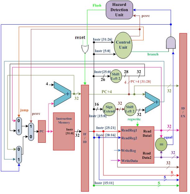
29 Figure
30 Testing (Prelab.) Test your design for the pipelined processor by filling the instruction memory by the instruction sequence shown in Table. Table. The Content of the Instruction Memory Address Instruction Machine Code LW R, 4(R) 8C4 h LW R, (R) LW R3, (R) 3 LW R4, 8(R) 4 NAND R5, R, R3 5 NORI R6, R5, 3 6 SUB R8, R4, R 7 JAL 8 XOR R7, R5, R6 9 SW R7, 8(R) J 9 ADDI R8, R8, SW R5, 4(R) 3 SW R6, 4(R) 4 BEQ R8, R3, -4 5 SUB R9, R8, R3 6 JR R3 7 OR R, R7, R9 8 SLT R, R9, R4 (Prelab.) Next, write a Verilog test module to test your processor module Your timing diagram should contain the following signals: a) PC (The output of the program counter). b) The output of IFID register. c) The output for the registers R5, R6, R7, R8, R9, R, R. d) The output of forwarding unit (ForwardA, ForwardB). e) The input and the output of hazard detection unit. Calculate number of cycles needed to execute the above code. 3
Lecture 3: The Processor (Chapter 4 of textbook) Chapter 4.1
 Chapter 4.1") Lecture 3: The Processor (Chapter 4 of textbook) Chapter 4.1 Introduction Chapter 4.1 Chapter 4.2 Review: MIPS (RISC) Design Principles Simplicity favors regularity fixed size instructions small number
Lecture 3: The Processor (Chapter 4 of textbook) Chapter 4.1 Introduction Chapter 4.1 Chapter 4.2 Review: MIPS (RISC) Design Principles Simplicity favors regularity fixed size instructions small number
Chapter 4 The Processor 1. Chapter 4A. The Processor
 Chapter 4 The Processor 1 Chapter 4A The Processor Chapter 4 The Processor 2 Introduction CPU performance factors Instruction count Determined by ISA and compiler CPI and Cycle time Determined by CPU hardware
The Processor. Z. Jerry Shi Department of Computer Science and Engineering University of Connecticut. CSE3666: Introduction to Computer Architecture
 The Processor Z. Jerry Shi Department of Computer Science and Engineering University of Connecticut CSE3666: Introduction to Computer Architecture Introduction CPU performance factors Instruction count
ECS 154B Computer Architecture II Spring 2009
 ECS 154B Computer Architecture II Spring 2009 Pipelining Datapath and Control 6.2-6.3 Partially adapted from slides by Mary Jane Irwin, Penn State And Kurtis Kredo, UCD Pipelined CPU Break execution into
CENG 3420 Computer Organization and Design. Lecture 06: MIPS Processor - I. Bei Yu
 CENG 342 Computer Organization and Design Lecture 6: MIPS Processor - I Bei Yu CEG342 L6. Spring 26 The Processor: Datapath & Control q We're ready to look at an implementation of the MIPS q Simplified
CENG 3420 Lecture 06: Datapath
 CENG 342 Lecture 6: Datapath Bei Yu byu@cse.cuhk.edu.hk CENG342 L6. Spring 27 The Processor: Datapath & Control q We're ready to look at an implementation of the MIPS q Simplified to contain only: memory-reference
LECTURE 5. Single-Cycle Datapath and Control
 LECTURE 5 Single-Cycle Datapath and Control PROCESSORS In lecture 1, we reminded ourselves that the datapath and control are the two components that come together to be collectively known as the processor.
Processor (I) - datapath & control. Hwansoo Han
 - datapath & control. Hwansoo Han") Processor (I) - datapath & control Hwansoo Han Introduction CPU performance factors Instruction count - Determined by ISA and compiler CPI and Cycle time - Determined by CPU hardware We will examine two
Processor (I) - datapath & control Hwansoo Han Introduction CPU performance factors Instruction count - Determined by ISA and compiler CPI and Cycle time - Determined by CPU hardware We will examine two
Chapter 4. The Processor
 Chapter 4 The Processor Introduction CPU performance factors Instruction count Determined by ISA and compiler CPI and Cycle time Determined by CPU hardware We will examine two MIPS implementations A simplified
COMPUTER ORGANIZATION AND DESIGN. 5 th Edition. The Hardware/Software Interface. Chapter 4. The Processor
 COMPUTER ORGANIZATION AND DESIGN The Hardware/Software Interface 5 th Edition Chapter 4 The Processor COMPUTER ORGANIZATION AND DESIGN The Hardware/Software Interface 5 th Edition The Processor - Introduction
Chapter 4. Instruction Execution. Introduction. CPU Overview. Multiplexers. Chapter 4 The Processor 1. The Processor.
 COMPUTER ORGANIZATION AND DESIGN The Hardware/Software Interface 5 th Edition COMPUTER ORGANIZATION AND DESIGN The Hardware/Software Interface 5 th Edition Chapter 4 The Processor The Processor - Introduction
COMPUTER ORGANIZATION AND DESIGN. The Hardware/Software Interface. Chapter 4. The Processor: A Based on P&H
 COMPUTER ORGANIZATION AND DESIGN The Hardware/Software Interface Chapter 4 The Processor: A Based on P&H Introduction We will examine two MIPS implementations A simplified version A more realistic pipelined
COMPUTER ORGANIZATION AND DESIGN. 5 th Edition. The Hardware/Software Interface. Chapter 4. The Processor
 COMPUTER ORGANIZATION AND DESIGN The Hardware/Software Interface 5 th Edition Chapter 4 The Processor Introduction CPU performance factors Instruction count Determined by ISA and compiler CPI and Cycle
COMPUTER ORGANIZATION AND DESIGN
 COMPUTER ORGANIZATION AND DESIGN 5 Edition th The Hardware/Software Interface Chapter 4 The Processor 4.1 Introduction Introduction CPU performance factors Instruction count CPI and Cycle time Determined
Computer Organization and Structure. Bing-Yu Chen National Taiwan University
 Computer Organization and Structure Bing-Yu Chen National Taiwan University The Processor Logic Design Conventions Building a Datapath A Simple Implementation Scheme An Overview of Pipelining Pipelined
COMPUTER ORGANIZATION AND DESIGN
 COMPUTER ORGANIZATION AND DESIGN The Hardware/Software Interface 5 th Edition Chapter 4 The Processor Introduction CPU performance factors Instruction count Determined by ISA and compiler CPI and Cycle
Chapter 4. The Processor. Computer Architecture and IC Design Lab
 Chapter 4 The Processor Introduction CPU performance factors CPI Clock Cycle Time Instruction count Determined by ISA and compiler CPI and Cycle time Determined by CPU hardware We will examine two MIPS
CSEN 601: Computer System Architecture Summer 2014
 CSEN 601: Computer System Architecture Summer 2014 Practice Assignment 5 Solutions Exercise 5-1: (Midterm Spring 2013) a. What are the values of the control signals (except ALUOp) for each of the following
ELEC 5200/6200 Computer Architecture and Design Spring 2017 Lecture 4: Datapath and Control
 ELEC 52/62 Computer Architecture and Design Spring 217 Lecture 4: Datapath and Control Ujjwal Guin, Assistant Professor Department of Electrical and Computer Engineering Auburn University, Auburn, AL 36849
Systems Architecture
 Systems Architecture Lecture 15: A Simple Implementation of MIPS Jeremy R. Johnson Anatole D. Ruslanov William M. Mongan Some or all figures from Computer Organization and Design: The Hardware/Software
Lecture 4: Review of MIPS. Instruction formats, impl. of control and datapath, pipelined impl.
 Lecture 4: Review of MIPS Instruction formats, impl. of control and datapath, pipelined impl. 1 MIPS Instruction Types Data transfer: Load and store Integer arithmetic/logic Floating point arithmetic Control
CS3350B Computer Architecture Quiz 3 March 15, 2018
 CS3350B Computer Architecture Quiz 3 March 15, 2018 Student ID number: Student Last Name: Question 1.1 1.2 1.3 2.1 2.2 2.3 Total Marks The quiz consists of two exercises. The expected duration is 30 minutes.
Pipelined datapath Staging data. CS2504, Spring'2007 Dimitris Nikolopoulos
 Pipelined datapath Staging data b 55 Life of a load in the MIPS pipeline Note: both the instruction and the incremented PC value need to be forwarded in the next stage (in case the instruction is a beq)
Pipelining Analogy. Pipelined laundry: overlapping execution. Parallelism improves performance. Four loads: Non-stop: Speedup = 8/3.5 = 2.3.
 Pipelining Analogy Pipelined laundry: overlapping execution Parallelism improves performance Four loads: Speedup = 8/3.5 = 2.3 Non-stop: Speedup =2n/05n+15 2n/0.5n 1.5 4 = number of stages 4.5 An Overview
Lab 7 (All Sections) Prelab: Verilog Review and ALU Datapath and Control
 Prelab: Verilog Review and ALU Datapath and Control") Lab 7 (All Sections) Prelab: Verilog Review and ALU Datapath and Control Name: Sign the following statement: On my honor, as an Aggie, I have neither given nor received unauthorized aid on this academic
Lab 7 (All Sections) Prelab: Verilog Review and ALU Datapath and Control Name: Sign the following statement: On my honor, as an Aggie, I have neither given nor received unauthorized aid on this academic
The Processor (1) Jinkyu Jeong Computer Systems Laboratory Sungkyunkwan University
 Jinkyu Jeong Computer Systems Laboratory Sungkyunkwan University") The Processor (1) Jinkyu Jeong (jinkyu@skku.edu) Computer Systems Laboratory Sungkyunkwan University http://csl.skku.edu EEE3050: Theory on Computer Architectures, Spring 2017, Jinkyu Jeong (jinkyu@skku.edu)
The Processor (1) Jinkyu Jeong (jinkyu@skku.edu) Computer Systems Laboratory Sungkyunkwan University http://csl.skku.edu EEE3050: Theory on Computer Architectures, Spring 2017, Jinkyu Jeong (jinkyu@skku.edu)
4. What is the average CPI of a 1.4 GHz machine that executes 12.5 million instructions in 12 seconds?
 Chapter 4: Assessing and Understanding Performance 1. Define response (execution) time. 2. Define throughput. 3. Describe why using the clock rate of a processor is a bad way to measure performance. Provide
Codeword[1] Codeword[0]
![Codeword[1] Codeword[0]](/thumbs/96/127722826.jpg "Codeword[1] Codeword[0]") Student #: ID: A CSE 221 - Quiz 3 - Fall 29 Problem 1. Convolutional encoding is commonly used on cell phones to ensure data is received with few errors using the low transmit power typically available
Student #: ID: A CSE 221 - Quiz 3 - Fall 29 Problem 1. Convolutional encoding is commonly used on cell phones to ensure data is received with few errors using the low transmit power typically available
Lecture 9. Pipeline Hazards. Christos Kozyrakis Stanford University
 Lecture 9 Pipeline Hazards Christos Kozyrakis Stanford University http://eeclass.stanford.edu/ee18b 1 Announcements PA-1 is due today Electronic submission Lab2 is due on Tuesday 2/13 th Quiz1 grades will
COMPUTER ORGANIZATION AND DESIGN The Hardware/Software Interface. 5 th. Edition. Chapter 4. The Processor
 COMPUTER ORGANIZATION AND DESIGN The Hardware/Software Interface 5 th Edition Chapter 4 The Processor Introduction CPU performance factors Instruction count Determined by ISA and compiler CPI and Cycle
Processor Design Pipelined Processor (II) Hung-Wei Tseng
 Hung-Wei Tseng") Processor Design Pipelined Processor (II) Hung-Wei Tseng Recap: Pipelining Break up the logic with pipeline registers into pipeline stages Each pipeline registers is clocked Each pipeline stage takes one
Processor Design Pipelined Processor (II) Hung-Wei Tseng Recap: Pipelining Break up the logic with pipeline registers into pipeline stages Each pipeline registers is clocked Each pipeline stage takes one
CS Computer Architecture Spring Week 10: Chapter
 CS 35101 Computer Architecture Spring 2008 Week 10: Chapter 5.1-5.3 Materials adapated from Mary Jane Irwin (www.cse.psu.edu/~mji) and Kevin Schaffer [adapted from D. Patterson slides] CS 35101 Ch 5.1
CSE Quiz 3 - Fall 2009
 Student #: ID: B CSE 221 - Quiz 3 - Fall 29 Problem 1. (a) Enter an appropriate value in each table cell corresponding to the Instruction in the column. Enter an X if the value is not applicable for the
Design of Digital Circuits 2017 Srdjan Capkun Onur Mutlu (Guest starring: Frank K. Gürkaynak and Aanjhan Ranganathan)
") Microarchitecture Design of Digital Circuits 27 Srdjan Capkun Onur Mutlu (Guest starring: Frank K. Gürkaynak and Aanjhan Ranganathan) http://www.syssec.ethz.ch/education/digitaltechnik_7 Adapted from Digital
Microarchitecture Design of Digital Circuits 27 Srdjan Capkun Onur Mutlu (Guest starring: Frank K. Gürkaynak and Aanjhan Ranganathan) http://www.syssec.ethz.ch/education/digitaltechnik_7 Adapted from Digital
CPE 335 Computer Organization. Basic MIPS Architecture Part I
 CPE 335 Computer Organization Basic MIPS Architecture Part I Dr. Iyad Jafar Adapted from Dr. Gheith Abandah slides http://www.abandah.com/gheith/courses/cpe335_s8/index.html CPE232 Basic MIPS Architecture
Laboratory Exercise 6 Pipelined Processors 0.0
 Laboratory Exercise 6 Pipelined Processors 0.0 Goals After this laboratory exercise, you should understand the basic principles of how pipelining works, including the problems of data and branch hazards
Chapter 4 The Processor 1. Chapter 4B. The Processor
 Chapter 4 The Processor 1 Chapter 4B The Processor Chapter 4 The Processor 2 Control Hazards Branch determines flow of control Fetching next instruction depends on branch outcome Pipeline can t always
CC 311- Computer Architecture. The Processor - Control
 CC 311- Computer Architecture The Processor - Control Control Unit Functions: Instruction code Control Unit Control Signals Select operations to be performed (ALU, read/write, etc.) Control data flow (multiplexor
Chapter 5 Solutions: For More Practice
 Chapter 5 Solutions: For More Practice 1 Chapter 5 Solutions: For More Practice 5.4 Fetching, reading registers, and writing the destination register takes a total of 300ps for both floating point add/subtract
CS/COE0447: Computer Organization
 CS/COE0447: Computer Organization and Assembly Language Datapath and Control Sangyeun Cho Dept. of Computer Science A simple MIPS We will design a simple MIPS processor that supports a small instruction
CS/COE0447: Computer Organization
 A simple MIPS CS/COE447: Computer Organization and Assembly Language Datapath and Control Sangyeun Cho Dept. of Computer Science We will design a simple MIPS processor that supports a small instruction
COMPUTER ORGANIZATION AND DESIGN
 ARM COMPUTER ORGANIZATION AND DESIGN Edition The Hardware/Software Interface Chapter 4 The Processor Modified and extended by R.J. Leduc - 2016 To understand this chapter, you will need to understand some
ECE473 Computer Architecture and Organization. Pipeline: Data Hazards
 Computer Architecture and Organization Pipeline: Data Hazards Lecturer: Prof. Yifeng Zhu Fall, 2015 Portions of these slides are derived from: Dave Patterson UCB Lec 14.1 Pipelining Outline Introduction
Chapter 4. The Processor
 Chapter 4 The Processor Introduction CPU performance factors Instruction count Determined by ISA and compiler CPI and Cycle time Determined by CPU hardware We will examine two MIPS implementations A simplified
 --------------------------------------------------------------------------------------------------------------------- 1. Objectives: Using the Logisim simulator Designing and testing a Pipelined 16-bit
COMP2611: Computer Organization. The Pipelined Processor
 COMP2611: Computer Organization The 1 2 Background 2 High-Performance Processors 3 Two techniques for designing high-performance processors by exploiting parallelism: Multiprocessing: parallelism among
Topic #6. Processor Design
 Topic #6 Processor Design Major Goals! To present the single-cycle implementation and to develop the student's understanding of combinational and clocked sequential circuits and the relationship between
The MIPS Processor Datapath
 The MIPS Processor Datapath Module Outline MIPS datapath implementation Register File, Instruction memory, Data memory Instruction interpretation and execution. Combinational control Assignment: Datapath
EE557--FALL 1999 MAKE-UP MIDTERM 1. Closed books, closed notes
 NAME: STUDENT NUMBER: EE557--FALL 1999 MAKE-UP MIDTERM 1 Closed books, closed notes Q1: /1 Q2: /1 Q3: /1 Q4: /1 Q5: /15 Q6: /1 TOTAL: /65 Grade: /25 1 QUESTION 1(Performance evaluation) 1 points We are
CPU Organization (Design)
") ISA Requirements CPU Organization (Design) Datapath Design: Capabilities & performance characteristics of principal Functional Units (FUs) needed by ISA instructions (e.g., Registers, ALU, Shifters, Logic
ISA Requirements CPU Organization (Design) Datapath Design: Capabilities & performance characteristics of principal Functional Units (FUs) needed by ISA instructions (e.g., Registers, ALU, Shifters, Logic
CS232 Final Exam May 5, 2001
 CS232 Final Exam May 5, 2 Name: This exam has 4 pages, including this cover. There are six questions, worth a total of 5 points. You have 3 hours. Budget your time! Write clearly and show your work. State
CENG 3420 Lecture 06: Pipeline
 CENG 3420 Lecture 06: Pipeline Bei Yu byu@cse.cuhk.edu.hk CENG3420 L06.1 Spring 2019 Outline q Pipeline Motivations q Pipeline Hazards q Exceptions q Background: Flip-Flop Control Signals CENG3420 L06.2
Department of Computer and IT Engineering University of Kurdistan. Computer Architecture Pipelining. By: Dr. Alireza Abdollahpouri
 Department of Computer and IT Engineering University of Kurdistan Computer Architecture Pipelining By: Dr. Alireza Abdollahpouri Pipelined MIPS processor Any instruction set can be implemented in many
Digital Design & Computer Architecture (E85) D. Money Harris Fall 2007
 D. Money Harris Fall 2007") Digital Design & Computer Architecture (E85) D. Money Harris Fall 2007 Final Exam This is a closed-book take-home exam. You are permitted a calculator and two 8.5x sheets of paper with notes. The exam
Digital Design & Computer Architecture (E85) D. Money Harris Fall 2007 Final Exam This is a closed-book take-home exam. You are permitted a calculator and two 8.5x sheets of paper with notes. The exam
Chapter 5: The Processor: Datapath and Control
 Chapter 5: The Processor: Datapath and Control Overview Logic Design Conventions Building a Datapath and Control Unit Different Implementations of MIPS instruction set A simple implementation of a processor
Pipelining. Ideal speedup is number of stages in the pipeline. Do we achieve this? 2. Improve performance by increasing instruction throughput ...
 CHAPTER 6 1 Pipelining Instruction class Instruction memory ister read ALU Data memory ister write Total (in ps) Load word 200 100 200 200 100 800 Store word 200 100 200 200 700 R-format 200 100 200 100
Outline. A pipelined datapath Pipelined control Data hazards and forwarding Data hazards and stalls Branch (control) hazards Exception
 hazards Exception") Outline A pipelined datapath Pipelined control Data hazards and forwarding Data hazards and stalls Branch (control) hazards Exception 1 4 Which stage is the branch decision made? Case 1: 0 M u x 1 Add
Outline A pipelined datapath Pipelined control Data hazards and forwarding Data hazards and stalls Branch (control) hazards Exception 1 4 Which stage is the branch decision made? Case 1: 0 M u x 1 Add
Computer Architecture, IFE CS and T&CS, 4 th sem. Single-Cycle Architecture
 Single-Cycle Architecture Data flow Data flow is synchronized with clock (edge) in sequential systems Architecture Elements - assumptions Program (Instruction) memory: All instructions & buses are 32-bit
RISC Processor Design
 RISC Processor Design Single Cycle Implementation - MIPS Virendra Singh Indian Institute of Science Bangalore virendra@computer.org Lecture 13 SE-273: Processor Design Feb 07, 2011 SE-273@SERC 1 Courtesy:
Chapter 4. The Processor. Instruction count Determined by ISA and compiler. We will examine two MIPS implementations
 Chapter 4 The Processor Part I Introduction CPU performance factors Instruction count Determined by ISA and compiler CPI and Cycle time Determined by CPU hardware We will examine two MIPS implementations
EE557--FALL 1999 MIDTERM 1. Closed books, closed notes
 NAME: SOLUTIONS STUDENT NUMBER: EE557--FALL 1999 MIDTERM 1 Closed books, closed notes GRADING POLICY: The front page of your exam shows your total numerical score out of 75. The highest numerical score
Chapter 4. The Processor
 Chapter 4 The Processor Introduction CPU performance factors Instruction count Determined by ISA and compiler CPI and Cycle time Determined by CPU hardware 4.1 Introduction We will examine two MIPS implementations
Review: Abstract Implementation View
 Review: Abstract Implementation View Split memory (Harvard) model - single cycle operation Simplified to contain only the instructions: memory-reference instructions: lw, sw arithmetic-logical instructions:
Computer and Information Sciences College / Computer Science Department Enhancing Performance with Pipelining
 Computer and Information Sciences College / Computer Science Department Enhancing Performance with Pipelining Single-Cycle Design Problems Assuming fixed-period clock every instruction datapath uses one
14:332:331 Pipelined Datapath
 14:332:331 Pipelined Datapath I n s t r. O r d e r Inst 0 Inst 1 Inst 2 Inst 3 Inst 4 Single Cycle Disadvantages & Advantages Uses the clock cycle inefficiently the clock cycle must be timed to accommodate
CPE 335 Computer Organization. Basic MIPS Pipelining Part I
 CPE 335 Computer Organization Basic MIPS Pipelining Part I Dr. Iyad Jafar Adapted from Dr. Gheith Abandah slides http://www.abandah.com/gheith/courses/cpe335_s08/index.html CPE232 Basic MIPS Pipelining
ECE 313 Computer Organization FINAL EXAM December 14, This exam is open book and open notes. You have 2 hours.
 This exam is open book and open notes. You have 2 hours. Problems 1-4 refer to a proposed MIPS instruction lwu (load word - update) which implements update addressing an addressing mode that is used in
Lecture Topics. Announcements. Today: Data and Control Hazards (P&H ) Next: continued. Exam #1 returned. Milestone #5 (due 2/27)
 Next: continued. Exam #1 returned. Milestone #5 (due 2/27)") Lecture Topics Today: Data and Control Hazards (P&H 4.7-4.8) Next: continued 1 Announcements Exam #1 returned Milestone #5 (due 2/27) Milestone #6 (due 3/13) 2 1 Review: Pipelined Implementations Pipelining
Lecture Topics Today: Data and Control Hazards (P&H 4.7-4.8) Next: continued 1 Announcements Exam #1 returned Milestone #5 (due 2/27) Milestone #6 (due 3/13) 2 1 Review: Pipelined Implementations Pipelining
CPE 335. Basic MIPS Architecture Part II
 CPE 335 Computer Organization Basic MIPS Architecture Part II Dr. Iyad Jafar Adapted from Dr. Gheith Abandah slides http://www.abandah.com/gheith/courses/cpe335_s08/index.html CPE232 Basic MIPS Architecture
CSEE 3827: Fundamentals of Computer Systems
 CSEE 3827: Fundamentals of Computer Systems Lecture 21 and 22 April 22 and 27, 2009 martha@cs.columbia.edu Amdahl s Law Be aware when optimizing... T = improved Taffected improvement factor + T unaffected
CS 351 Exam 2 Mon. 11/2/2015
 CS 351 Exam 2 Mon. 11/2/2015 Name: Rules and Hints The MIPS cheat sheet and datapath diagram are attached at the end of this exam for your reference. You may use one handwritten 8.5 11 cheat sheet (front
Processor (II) - pipelining. Hwansoo Han
 - pipelining. Hwansoo Han") Processor (II) - pipelining Hwansoo Han Pipelining Analogy Pipelined laundry: overlapping execution Parallelism improves performance Four loads: Speedup = 8/3.5 =2.3 Non-stop: 2n/0.5n + 1.5 4 = number
Processor (II) - pipelining Hwansoo Han Pipelining Analogy Pipelined laundry: overlapping execution Parallelism improves performance Four loads: Speedup = 8/3.5 =2.3 Non-stop: 2n/0.5n + 1.5 4 = number
Chapter 4. The Processor
 Chapter 4 The Processor Introduction CPU performance factors Instruction count Determined by ISA and compiler CPI and Cycle time Determined by CPU hardware We will examine two MIPS implementations A simplified
ECE260: Fundamentals of Computer Engineering
 Datapath for a Simplified Processor James Moscola Dept. of Engineering & Computer Science York College of Pennsylvania Based on Computer Organization and Design, 5th Edition by Patterson & Hennessy Introduction
ENGN1640: Design of Computing Systems Topic 04: Single-Cycle Processor Design
 ENGN64: Design of Computing Systems Topic 4: Single-Cycle Processor Design Professor Sherief Reda http://scale.engin.brown.edu Electrical Sciences and Computer Engineering School of Engineering Brown University
Design a MIPS Processor (2/2)
") 93-2Digital System Design Design a MIPS Processor (2/2) Lecturer: Chihhao Chao Advisor: Prof. An-Yeu Wu 2005/5/13 Friday ACCESS IC LABORTORY Outline v 6.1 An Overview of Pipelining v 6.2 A Pipelined Datapath
93-2Digital System Design Design a MIPS Processor (2/2) Lecturer: Chihhao Chao Advisor: Prof. An-Yeu Wu 2005/5/13 Friday ACCESS IC LABORTORY Outline v 6.1 An Overview of Pipelining v 6.2 A Pipelined Datapath
ECE232: Hardware Organization and Design
 ECE232: Hardware Organization and Design Lecture 14: One Cycle MIPs Datapath Adapted from Computer Organization and Design, Patterson & Hennessy, UCB R-Format Instructions Read two register operands Perform
Computer Science 324 Computer Architecture Mount Holyoke College Fall Topic Notes: Data Paths and Microprogramming
 Computer Science 324 Computer Architecture Mount Holyoke College Fall 2007 Topic Notes: Data Paths and Microprogramming We have spent time looking at the MIPS instruction set architecture and building
CSE 378 Midterm 2/12/10 Sample Solution
 Question 1. (6 points) (a) Rewrite the instruction sub $v0,$t8,$a2 using absolute register numbers instead of symbolic names (i.e., if the instruction contained $at, you would rewrite that as $1.) sub
EECS150 - Digital Design Lecture 10- CPU Microarchitecture. Processor Microarchitecture Introduction
 EECS150 - Digital Design Lecture 10- CPU Microarchitecture Feb 18, 2010 John Wawrzynek Spring 2010 EECS150 - Lec10-cpu Page 1 Processor Microarchitecture Introduction Microarchitecture: how to implement
Design of the MIPS Processor
 Design of the MIPS Processor We will study the design of a simple version of MIPS that can support the following instructions: I-type instructions LW, SW R-type instructions, like ADD, SUB Conditional
Single Cycle CPU Design. Mehran Rezaei
 Single Cycle CPU Design Mehran Rezaei What does it mean? Instruction Fetch Instruction Memory clk pc 32 32 address add $t,$t,$t2 instruction Next Logic to generate the address of next instruction The Branch
The Processor: Datapath and Control. Jin-Soo Kim Computer Systems Laboratory Sungkyunkwan University
 The Processor: Datapath and Control Jin-Soo Kim (jinsookim@skku.edu) Computer Systems Laboratory Sungkyunkwan University http://csl.skku.edu Introduction CPU performance factors Instruction count Determined
Full Datapath. Chapter 4 The Processor 2
 Pipelining Full Datapath Chapter 4 The Processor 2 Datapath With Control Chapter 4 The Processor 3 Performance Issues Longest delay determines clock period Critical path: load instruction Instruction memory
Lecture 8: Control COS / ELE 375. Computer Architecture and Organization. Princeton University Fall Prof. David August
 Lecture 8: Control COS / ELE 375 Computer Architecture and Organization Princeton University Fall 2015 Prof. David August 1 Datapath and Control Datapath The collection of state elements, computation elements,
Single Cycle Data Path
 Single ycle ata Path S 365 Lecture 6 Prof. Yih Huang S365 1 MIPS Lite We're ready to look at an implementation of the MIPS Simplified to support only: memory-reference instructions: lw, sw arithmetic-logical
LECTURE 9. Pipeline Hazards
 LECTURE 9 Pipeline Hazards PIPELINED DATAPATH AND CONTROL In the previous lecture, we finalized the pipelined datapath for instruction sequences which do not include hazards of any kind. Remember that
The Processor: Datapath & Control
 Orange Coast College Business Division Computer Science Department CS 116- Computer Architecture The Processor: Datapath & Control Processor Design Step 3 Assemble Datapath Meeting Requirements Build the
Chapter 4. The Processor
 Chapter 4 The Processor Recall. ISA? Instruction Fetch Instruction Decode Operand Fetch Execute Result Store Next Instruction Instruction Format or Encoding how is it decoded? Location of operands and
ECE260: Fundamentals of Computer Engineering
 Data Hazards in a Pipelined Datapath James Moscola Dept. of Engineering & Computer Science York College of Pennsylvania Based on Computer Organization and Design, 5th Edition by Patterson & Hennessy Data
Data paths for MIPS instructions
 You are familiar with how MIPS programs step from one instruction to the next, and how branches can occur conditionally or unconditionally. We next examine the machine level representation of how MIPS
EECS 151/251A Fall 2017 Digital Design and Integrated Circuits. Instructor: John Wawrzynek and Nicholas Weaver. Lecture 13 EE141
 EECS 151/251A Fall 2017 Digital Design and Integrated Circuits Instructor: John Wawrzynek and Nicholas Weaver Lecture 13 Project Introduction You will design and optimize a RISC-V processor Phase 1: Design
COMP303 - Computer Architecture Lecture 8. Designing a Single Cycle Datapath
 COMP33 - Computer Architecture Lecture 8 Designing a Single Cycle Datapath The Big Picture The Five Classic Components of a Computer Processor Input Control Memory Datapath Output The Big Picture: The
Pipeline Hazards. Jin-Soo Kim Computer Systems Laboratory Sungkyunkwan University
 Pipeline Hazards Jin-Soo Kim (jinsookim@skku.edu) Computer Systems Laboratory Sungkyunkwan University http://csl.skku.edu Hazards What are hazards? Situations that prevent starting the next instruction
ECEN 651: Microprogrammed Control of Digital Systems Department of Electrical and Computer Engineering Texas A&M University
 ECEN 651: Microprogrammed Control of Digital Systems Department of Electrical and Computer Engineering Texas A&M University Prof. Mi Lu TA: Ehsan Rohani Laboratory Exercise #8 Dynamic Branch Prediction
ECE369. Chapter 5 ECE369
 Chapter 5 1 State Elements Unclocked vs. Clocked Clocks used in synchronous logic Clocks are needed in sequential logic to decide when an element that contains state should be updated. State element 1
Pipelined Processor Design
 Pipelined Processor Design Pipelined Implementation: MIPS Virendra Singh Computer Design and Test Lab. Indian Institute of Science (IISc) Bangalore virendra@computer.org Advance Computer Architecture http://www.serc.iisc.ernet.in/~viren/courses/aca/aca.htm
Chapter 4. The Processor
 Chapter 4 The Processor 1 Introduction CPU performance factors Instruction count Determined by ISA and compiler CPI and Cycle time Determined by CPU hardware We will examine two MIPS implementations A
CS/CoE 1541 Exam 1 (Spring 2019).
.") CS/CoE 1541 Exam 1 (Spring 2019). Name: Question 1 (8+2+2+3=15 points): In this problem, consider the execution of the following code segment on a 5-stage pipeline with forwarding/stalling hardware and
CS/CoE 1541 Exam 1 (Spring 2019). Name: Question 1 (8+2+2+3=15 points): In this problem, consider the execution of the following code segment on a 5-stage pipeline with forwarding/stalling hardware and
ﻪﺘﻓﺮﺸﻴﭘ ﺮﺗﻮﻴﭙﻣﺎﻛ يرﺎﻤﻌﻣ MIPS يرﺎﻤﻌﻣ data path and ontrol control
 معماري كامپيوتر پيشرفته معماري MIPS data path and control abbasi@basu.ac.ir Topics Building a datapath support a subset of the MIPS-I instruction-set A single cycle processor datapath all instruction actions