UNIT 5. Microcontrollers. Syllabus
|
|
|
- Cecil Quinn
- 5 years ago
- Views:
Transcription
1 UNIT 5 Microcontrollers Syllabus Architecture of 8051 Signals Operational features Memory and I/O addressing Interrupts Instruction set Applications.
2 OVERVIEW The past three decades have seen the introduction of a technology that has radically changed the way in which we analyze and control the world around us. Born of parallel developments in computer architecture and integrated circuit fabrication, the microprocessor or computer on chip first became a commercial reality in 1971 with the introduction of 4 bit 4004 by a small, unknown company by the name of Intel Corporation. Other, more well established semiconductor firms soon followed Intel s pioneering technology so that by the late 1970s we could choose from a half dozen or so microprocessor types. The 1970s also saw the growth of the number of personal computer users from a handful of hobbyists and hackers to million of business, industrial, governmental, defense, educational and private users now enjoying the advantages of inexpensive computing. A by product of microprocessor development was the microcontroller. The same fabrication techniques and programming concepts that make possible the general purpose microprocessor also yielded the microcontroller. Microcontrollers are not as well known to the general public. The public is however very well aware that something is responsible for all of the smart DVDs, clock radio, washer, dryer, video games, telephones, microwaves, TVs, automobiles, toys, copiers, elevators, vending machines, irons etc. Companies are also aware that being competitive in this age of micro chip requires their products, the machinery they used to make those products, to have some smarts. The purpose of this unit is to introduce the concept of microcontroller and discuss current trends. Specifically, we are going to concentrate one of the most popular microcontroller, 8051 in detail.
3 LEARNING OBJECTIVES Describe the hardware features of the 8051 microcontroller List the internal registers of the 8051 microcontroller and their functions State the physical differences between the port 0, 1, 2 and 3 I/O pins Describe various operating modes of timer/counter and associated control registers Describe the various operating modes of UART and associated control registers List the type of interrupts, interrupt program address and interrupt control registers

4 Microcontrollers Microcontroller manufacturers have been competing for a long time for attracting choosy customers and every couple of days a new chip with a higher operating frequency, more memory and upgraded A/D converters appeared on the market. However, most of them had the same or at least very similar architecture known in the world of microcontrollers as 8051 compatible. What is all this about? The whole story has its beginnings in the far 80s when Intel launched the first series of microcontrollers called the MCS 051. Even though these microcontrollers had quite modest features in comparison to the new ones, they conquered the world very soon and became a standard for what nowadays is called the microcontroller. The main reason for their great success and popularity is a skillfully chosen configuration which satisfies different needs of a large number of users allowing at the same time constant expansions (refers to the new types of microcontrollers). Besides, the software has been developed in great extend in the meantime, and it simply was not profitable to change anything in the microcontroller s basic core. This is the reason for having a great number of various microcontrollers which basically are solely upgraded versions of the 8051 family. What makes this microcontroller so special and universal so that almost all manufacturers all over the world manufacture it today under different name?
5 As seen in figure above, the 8051 microcontroller has nothing impressive in appearance:4 Kb of ROM is not much at all. 128Kb of RAM (including SFRs) satisfies the user's basic needs. 4 ports having in total of 32 input/output lines are in most cases sufficient to make all necessary connections to peripheral environment. The whole configuration is obviously thought of as to satisfy the needs of most programmers working on development of automation devices. One of its advantages is that nothing is missing and nothing is too much. In other words, it is created exactly in accordance to the average user s taste and needs. Another advantages are RAM organization, the operation of Central Processor Unit (CPU) and ports which completely use all recourses and enable further upgrade. 2.2 Pinout Description Pins 1-8: Port 1 Each of these pins can be configured as an input or an output. Pin 9: RS A logic one on this pin disables the microcontroller and clears the contents of most registers. In other words, the positive voltage on this pin resets the microcontroller. By applying logic zero to this pin, the program starts execution from the beginning. Pins10-17: Port 3 Similar to port 1, each of these pins can serve as general input or output. Besides, all of them have alternative functions: Pin 10: RXD Serial asynchronous communication input or Serial synchronous communication output. Pin 11: TXD Serial asynchronous communication output or Serial synchronous communication clock output. Pin 12: INT0 Interrupt 0 input. Pin 13: INT1 Interrupt 1 input. Pin 14: T0 Counter 0 clock input. Pin 15: T1 Counter 1 clock input. Pin 16: WR Write to external (additional) RAM.
6 Pin 17: RD Read from external RAM. Pin 18, 19: X2, X1 Internal oscillator input and output. A quartz crystal which specifies operating frequency is usually connected to these pins. Instead of it, miniature ceramics resonators can also be used for frequency stability. Later versions of microcontrollers operate at a frequency of 0 Hz up to over 50 Hz. Pin 20: GND Ground. Pin 21-28: Port 2 If there is no intention to use external memory then these port pins are configured as general inputs/outputs. In case external memory is used, the higher address byte, i.e. addresses A8-A15 will appear on this port. Even though memory with capacity of 64Kb is not used, which means that not all eight port bits are used for its addressing, the rest of them are not available as inputs/outputs. Pin 29: PSEN If external ROM is used for storing program then a logic zero (0) appears on it every time the microcontroller reads a byte from memory. Pin 30: ALE Prior to reading from external memory, the microcontroller puts the lower address byte (A0-A7) on P0 and activates the ALE output. After receiving signal from the ALE pin, the external register (usually 74HCT373 or 74HCT375 add-on chip) memorizes the state of P0 and uses it as a memory chip address. Immediately after that, the ALU pin is returned its previous logic state and P0 is now used as a Data Bus. As seen, port data multiplexing is performed by means of only one additional (and cheap) integrated circuit. In other words, this port is used for both data and address transmission. Pin 31: EA By applying logic zero to this pin, P2 and P3 are used for data and address transmission with no regard to whether there is internal memory or not. It means that even there is a program written to the microcontroller, it will not be executed. Instead, the program written to external ROM will be executed. By applying logic one to the EA pin, the microcontroller will use both memories, first internal then external (if exists). Pin 32-39: Port 0 Similar to P2, if external memory is not used, these pins can be used as general inputs/outputs. Otherwise, P0 is configured as address output (A0-A7) when the ALE pin is driven high (1) or as data output (Data Bus) when the ALE pin is driven low (0). Pin 40: VCC +5V power supply.
 or an output (0), depends on its logic state.")
7 2.3 Input/Output Ports (I/O Ports) All 8051 microcontrollers have 4 I/O ports each comprising 8 bits which can be configured as inputs or outputs. Accordingly, in total of 32 input/output pins enabling the microcontroller to be connected to peripheral devices are available for use. Pin configuration, i.e. whether it is to be configured as an input (1) or an output (0), depends on its logic state. In order to configure a microcontroller pin as an input, it is necessary to apply a logic zero (0) to appropriate I/O port bit. In this case, voltage level on appropriate pin will be 0. Similarly, in order to configure a microcontroller pin as an input, it is necessary to apply a logic one (1) to appropriate port. In this case, voltage level on appropriate pin will be 5V (as is the case with any TTL input). This may seem confusing but don't loose your patience. It all becomes clear after studying simple electronic circuits connected to an I/O pin.

 is applied to a bit of the P register.")
8 Input/Output (I/O) pin Figure above illustrates a simplified schematic of all circuits within the microcontroler connected to one of its pins. It refers to all the pins except those of the P0 port which do not have pull-up resistors built-in. Output pin A logic zero (0) is applied to a bit of the P register. The output FE transistor is turned on, thus connecting the appropriate pin to ground.

9 Input pin A logic one (1) is applied to a bit of the P register. The output FE transistor is turned off and the appropriate pin remains connected to the power supply voltage over a pull-up resistor of high resistance. Logic state (voltage) of any pin can be changed or read at any moment. A logic zero (0) and logic one (1) are not equal. A logic one (0) represents a short circuit to ground. Such a pin acts as an output. A logic one (1) is loosely connected to the power supply voltage over a resistor of high resistance. Since this voltage can be easily reduced by an external signal, such a pin acts as an input. Port 0 The P0 port is characterized by two functions. If external memory is used then the lower address byte (addresses A0-A7) is applied on it. Otherwise, all bits of this port are configured as inputs/outputs. The other function is expressed when it is configured as an output. Unlike other ports consisting of pins with built-in pull-up resistor connected by its end to 5 V power supply, pins of this port have this resistor left out. This apparently small difference has its consequences: If any pin of this port is configured as an input then it acts as if it floats. Such an input has unlimited input resistance and indetermined potential.
 on this output pin, it is necessary to built in an external pull-up resistor.")
10 When the pin is configured as an output, it acts as an open drain. By applying logic 0 to a port bit, the appropriate pin will be connected to ground (0V). By applying logic 1, the external output will keep on floating. In order to apply logic 1 (5V) on this output pin, it is necessary to built in an external pull-up resistor. Only in case P0 is used for addressing external memory, the microcontroller will provide internal power supply source in order to supply its pins with logic one. There is no need to add external pull-up resistors. Port 1 P1 is a true I/O port, because it doesn't have any alternative functions as is the case with P0, but can be cofigured as general I/O only. It has a pull-up resistor built-in and is completely compatible with TTL circuits. Port 2 P2 acts similarly to P0 when external memory is used. Pins of this port occupy addresses intended for external memory chip. This time it is about the higher address byte with addresses A8-A15. When no memory is added, this port can be used as a general input/output port showing features similar to P1. Port 3 All port pins can be used as general I/O, but they also have an alternative function. In order to use these alternative functions, a logic one (1) must be applied to appropriate bit of the P3 register. In tems of hardware, this port is similar to P0, with the difference that its pins have a pull-up resistor built-in.
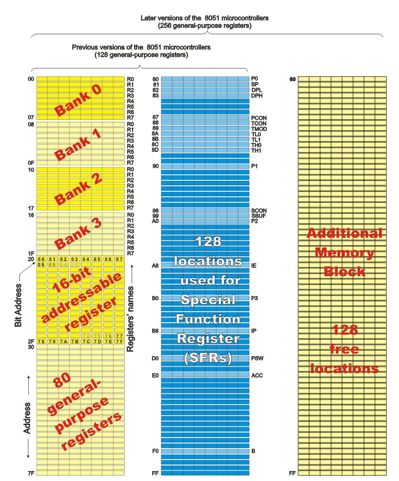
11 Pin's Current limitations When configured as outputs (logic zero (0)), single port pins can receive a current of 10mA. If all 8 bits of a port are active, a total current must be limited to 15mA (port P0: 26mA). If all ports (32 bits) are active, total maximum current must be limited to 71mA. When these pins are configured as inputs (logic 1), built-in pullup resistors provide very weak current, but strong enough to activate up to 4 TTL inputs of LS series. As seen from description of some ports, even though all of them have more or less similar architecture, it is necessary to pay attention to which of them is to be used for what and how. For example, if they shall be used as outputs with high voltage level (5V), then P0 should be avoided because its pins do not have pull-up resistors, thus giving low logic level only. When using other ports, one should have in mind that pull-up resistors have a relatively high resistance, so that their pins can give a current of several hundreds microamperes only. 2.4 Memory Organization The 8051 has two types of memory and these are Program Memory and Data Memory. Program Memory (ROM) is used to permanently save the program being executed, while Data Memory (RAM) is used for temporarily storing data and intermediate results created and used during the operation of the microcontroller. Depending on the model in use (we are still talking about the 8051 microcontroller family in general) at most a few Kb of ROM and 128 or 256 bytes of RAM is used. However All 8051 microcontrollers have a 16-bit addressing bus and are capable of addressing 64 kb memory. It is neither a mistake nor a big ambition of engineers who were working on basic core development. It is a matter of smart memory organization which makes these microcontrollers a real programmers goody. Program Memory The first models of the 8051 microcontroller family did not have internal program memory. It was added as an external separate chip. These models are recognizable by their label beginning with 803 (for example 8031 or 8032). All later models have

12 a few Kbyte ROM embedded. Even though such an amount of memory is sufficient for writing most of the programs, there are situations when it is necessary to use additional memory as well. A typical example are so called lookup tables. They are used in cases when equations describing some processes are too complicated or when there is no time for solving them. In such cases all necessary estimates and approximates are executed in advance and the final results are put in the tables (similar to logarithmic tables). How does the microcontroller handle external memory depends on the EA pin logic state:

13 EA=0 In this case, the microcontroller completely ignores internal program memory and executes only the program stored in external memory. EA=1 In this case, the microcontroller executes first the program from built-in ROM, then the program stored in external memory. In both cases, P0 and P2 are not available for use since being used for data and address transmission. Besides, the ALE and PSEN pins are also used. Data Memory As already mentioned, Data Memory is used for temporarily storing data and intermediate results created and used during the operation of the microcontroller. Besides, RAM memory built in the 8051 family includes many registers such as
14 hardware counters and timers, input/output ports, serial data buffers etc. The previous models had 256 RAM locations, while for the later models this number was incremented by additional 128 registers. However, the first 256 memory locations (addresses 0-FFh) are the heart of memory common to all the models belonging to the 8051 family. Locations available to the user occupy memory space with addresses 0-7Fh, i.e. first 128 registers. This part of RAM is divided in several blocks. The first block consists of 4 banks each including 8 registers denoted by R0-R7. Prior to accessing any of these registers, it is necessary to select the bank containing it. The next memory block (address 20h-2Fh) is bit- addressable, which means that each bit has its own address (0-7Fh). Since there are 16 such registers, this block contains in total of 128 bits with separate addresses (address of bit 0 of the 20h byte is 0, while address of bit 7 of the 2Fh byte is 7Fh). The third group of registers occupy addresses 2Fh-7Fh, i.e. 80 locations, and does not have any special functions or features. Additional RAM In order to satisfy the programmers constant hunger for Data Memory, the manufacturers decided to embed an additional memory block of 128 locations into the latest versions of the 8051 microcontrollers. However, it s not as simple as it seems to be The problem is that electronics performing addressing has 1 byte (8 bits) on disposal and is capable of reaching only the first 256 locations, therefore. In order to keep already existing 8-bit architecture and compatibility with other existing models a small trick was done. What does it mean? It means that additional memory block shares the same addresses with locations intended for the SFRs (80h- FFh). In order to differentiate between these two physically separated memory spaces, different ways of addressing are used. The SFRs memory locations are accessed by direct addressing, while additional RAM memory locations are accessed by indirect addressing.
15

16 Memory expansion In case memory (RAM or ROM) built in the microcontroller is not sufficient, it is possible to add two external memory chips with capacity of 64Kb each. P2 and P3 I/O ports are used for their addressing and data transmission. From the user s point of view, everything works quite simply when properly connected because most operations are performed by the microcontroller itself.
17 The 8051 microcontroller has two pins for data read RD#(P3.7) and PSEN#. The first one is used for reading data from external data memory (RAM), while the other is used for reading data from external program memory (ROM). Both pins are active low. A typical example of memory expansion by adding RAM and ROM chips (Hardward architecture), is shown in figure above. Even though additional memory is rarely used with the latest versions of the microcontrollers, we will describe in short what happens when memory chips are connected according to the previous schematic. The whole process described below is performed automatically. When the program during execution encounters an instruction which resides in external memory (ROM), the microcontroller will activate its control output ALE and set the first 8 bits of address (A0-A7) on P0. IC circuit 74HCT573 passes the first 8 bits to memory address pins. A signal on the ALE pin latches the IC circuit 74HCT573 and immediately afterwards 8 higher bits of address (A8-A15) appear on the port. In this way, a desired location of additional program memory is addressed. It is left over to read its content. Port P0 pins are configured as inputs, the PSEN pin is activated and the microcontroller reads from memory chip. Similar occurs when it is necessary to read location from external RAM. Addressing is performed in the same way, while read and write are performed via signals appearing on the control outputs RD (is short for read) or WR (is short for write). Addressing While operating, the processor processes data as per program instructions. Each instruction consists of two parts. One part describes WHAT should be done, while the other explains HOW to do it. The latter part can be a data (binary number) or the address at which the data is stored. Two ways of addressing are used for all 8051 microcontrollers depending on which part of memory should be accessed: Direct Addressing On direct addressing, the address of memory location containing data to be read is specified in instruction. The address may contain a number being changed during operation (variable). For example:
18 Since the address is only one byte in size (the largest number is 255), only the first 255 locations of RAM can be accessed this way. The first half of RAM is available for use, while another half is reserved for SFRs. MOV A,33h; Means: move a number from address 33 hex. to accumulator Indirect Addressing On indirect addressing, a register containing the address of another register is specified in instruction. Data to be used in the program is stored in the letter register. For example: Indirect addressing is only used for accessing RAM locations available for use (never for accessing SFRs). This is the only way of accessing all the latest versions of the microcontrollers with additional memory block (128 locations of RAM). Simply put, when the program encounters instruction sign and if the specified address is higher than 128 ( 7F hex.), the processor knows that indirect addressing is used and skips memory space reserved for SFRs. MOV A,@R0; Means: Store the value from the register whose address is in the R0 register into accumulator On indirect addressing, registers R0, R1 or Stack Pointer are used for specifying 8- bit addresses. Since only 8 bits are avilable, it is possible to access only registers of internal RAM this way (128 locations when speaking of previous models or 256 locations when speaking of latest models of microcontrollers). If an extra memory chip is added then the 16-bit DPTR Register (consisting of the registers DPTRL and DPTRH) is used for specifying address. In this way it is possible to access any location in the range of 64K. 2.5 Special Function Registers (SFRs) Special Function Registers (SFRs) are a sort of control table used for running and monitoring the operation of the microcontroller. Each of these registers as well as each bit they include, has its name, address in the scope of RAM and precisely defined purpose such as timer control, interrupt control, serial communication control etc. Even though there are 128 memory locations intended to be occupied by them, the basic core, shared by all types of 8051 microcontrollers, has only 21 such registers. Rest of locations are intensionally left unoccupied in order to enable the manufacturers to further develop microcontrollers keeping them compatible with the previous versions. It also enables programs written a long time ago for microcontrollers which are out of production now to be used today.

19 A Register (Accumulator) A register is a general-purpose register used for storing intermediate results obtained during operation. Prior to executing an instruction upon any number or operand it is necessary to store it in the accumulator first. All results obtained from arithmetical operations performed by the ALU are stored in the accumulator. Data to be moved from one register to another must go through the accumulator. In other words, the A register is the most commonly used register and it is impossible to imagine a microcontroller without it. More than half instructions used by the 8051 microcontroller use somehow the accumulator. B Register

20 Multiplication and division can be performed only upon numbers stored in the A and B registers. All other instructions in the program can use this register as a spare accumulator (A). During the process of writing a program, each register is called by its name so that their exact addresses are not of importance for the user. During compilation, their names will be automatically replaced by appropriate addresses. R Registers (R0-R7) This is a common name for 8 general-purpose registers (R0, R1, R2...R7). Even though they are not true SFRs, they deserve to be discussed here because of their purpose. They occupy 4 banks within RAM. Similar to the accumulator, they are used for temporary storing variables and intermediate results during operation. Which one of these banks is to be active depends on two bits of the PSW Register. Active bank is a bank the registers of which are currently used. The following example best illustrates the purpose of these registers. Suppose it is necessary to perform some arithmetical operations upon numbers previously stored in the R registers: (R1+R2) - (R3+R4). Obviously, a register for temporary storing results of addition is needed. This is how it looks in the program:
21 MOV A,R3; Means: move number from R3 into accumulator ADD A,R4; Means: add number from R4 to accumulator (result remains in accumulator) MOV R5,A; Means: temporarily move the result from accumulator into R5 MOV A,R1; Means: move number from R1 to accumulator ADD A,R2; Means: add number from R2 to accumulator SUBB A,R5; Means: subtract number from R5 (there are R3+R4) Program Status Word (PSW) Register PSW register is one of the most important SFRs. It contains several status bits that reflect the current state of the CPU. Besides, this register contains Carry bit, Auxiliary Carry, two register bank select bits, Overflow flag, parity bit and userdefinable status flag. P - Parity bit. If a number stored in the accumulator is even then this bit will be automatically set (1), otherwise it will be cleared (0). It is mainly used during data transmit and receive via serial communication. - Bit 1. This bit is intended to be used in the future versions of microcontrollers. OV Overflow occurs when the result of an arithmetical operation is larger than 255 and cannot be stored in one register. Overflow condition causes the OV bit to be set (1). Otherwise, it will be cleared (0). RS0, RS1 - Register bank select bits. These two bits are used to select one of four register banks of RAM. By setting and clearing these bits, registers R0-R7 are stored in one of four banks of RAM. RS1 RS Space RAM in Bank0 00h- 07h Bank1 08h- 0Fh Bank2 10h- 17h Bank3 18h- 1Fh
 auxiliary bit used for all arithmetical operations and shift instructions.")
22 F0 - Flag 0. This is a general-purpose bit available for use. AC - Auxiliary Carry Flag is used for BCD operations only. CY - Carry Flag is the (ninth) auxiliary bit used for all arithmetical operations and shift instructions. Data Pointer Register (DPTR) DPTR register is not a true one because it doesn't physically exist. It consists of two separate registers: DPH (Data Pointer High) and (Data Pointer Low). For this reason it may be treated as a 16-bit register or as two independent 8-bit registers. Their 16 bits are primarly used for external memory addressing. Besides, the DPTR Register is usually used for storing data and intermediate results. Stack Pointer (SP) Register A value stored in the Stack Pointer points to the first free stack address and permits stack availability. Stack pushes increment the value in the Stack Pointer by 1.
23 Likewise, stack pops decrement its value by 1. Upon any reset and power-on, the value 7 is stored in the Stack Pointer, which means that the space of RAM reserved for the stack starts at this location. If another value is written to this register, the entire Stack is moved to the new memory location. P0, P1, P2, P3 - Input/Output Registers If neither external memory nor serial communication system are used then 4 ports with in total of 32 input/output pins are available for connection to peripheral environment. Each bit within these ports affects the state and performance of appropriate pin of the microcontroller. Thus, bit logic state is reflected on appropriate pin as a voltage (0 or 5 V) and vice versa, voltage on a pin reflects the state of appropriate port bit. As mentioned, port bit state affects performance of port pins, i.e. whether they will be configured as inputs or outputs. If a bit is cleared (0), the appropriate pin will be configured as an output, while if it is set (1), the appropriate pin will be configured as an input. Upon reset and power-on, all port bits are set (1), which means that all appropriate pins will be configured as inputs. I/O ports are directly connected to the microcontroller pins. Accordingly, logic state of these registers can be checked by voltmeter and vice versa, voltage on the pins can be checked by inspecting their bits! 2.6 Counters and Timers As you already know, the microcontroller oscillator uses quartz crystal for its operation. As the frequency of this oscillator is precisely defined and very stable, pulses it generates are always of the same width, which makes them ideal for time measurement. Such crystals are also used in quartz watches. In order to measure time between two events it is sufficient to count up pulses coming from this oscillator. That is exactly what the timer does. If the timer is properly programmed, the value stored in its register will be incremented (or decremented) with each coming pulse, i.e. once per each machine cycle. A single machine-cycle instruction


24 lasts for 12 quartz oscillator periods, which means that by embedding quartz with oscillator frequency of 12MHz, a number stored in the timer register will be changed million times per second, i.e. each microsecond. The 8051 microcontroller has 2 timers/counters called T0 and T1. As their names suggest, their main purpose is to measure time and count external events. Besides, they can be used for generating clock pulses to be used in serial communication, so called Baud Rate. Timer T0 As seen in figure below, the timer T0 consists of two registers TH0 and TL0 representing a low and a high byte of one 16-digit binary number. Accordingly, if the content of the timer T0 is equal to 0 (T0=0) then both registers it consists of will contain 0. If the timer contains for example number 1000 (decimal), then the TH0 register (high byte) will contain the number 3, while the TL0 register (low byte) will contain decimal number 232. Formula used to calculate values in these two registers is very simple: TH TL0 = T

25 Matching the previous example it would be as follows: = 1000 Since the timer T0 is virtually 16-bit register, the largest value it can store is In case of exceeding this value, the timer will be automatically cleared and counting starts from 0. This condition is called an overflow. Two registers TMOD and TCON are closely connected to this timer and control its operation. TMOD Register (Timer Mode) The TMOD register selects the operational mode of the timers T0 and T1. As seen in figure below, the low 4 bits (bit0 - bit3) refer to the timer 0, while the high 4 bits (bit4 - bit7) refer to the timer 1. There are 4 operational modes and each of them is described herein. Bits of this register have the following function: GATE1 enables and disables Timer 1 by means of a signal brought to the INT1 pin (P3.3): o 1 - Timer 1 operates only if the INT1 bit is set. o 0 - Timer 1 operates regardless of the logic state of the INT1 bit. C/T1 selects pulses to be counted up by the timer/counter 1: o 1 - Timer counts pulses brought to the T1 pin (P3.5). o 0 - Timer counts pulses from internal oscillator. T1M1,T1M0 These two bits select the operational mode of the Timer 1. T1M1 T1M0 Mode Description
26 GATE0 enables and disables Timer 1 using a signal brought to the INT0 pin (P3.2): o 1 - Timer 0 operates only if the INT0 bit is set. o 0 - Timer 0 operates regardless of the logic state of the INT0 bit. C/T0 selects pulses to be counted up by the timer/counter 0: o 1 - Timer counts pulses brought to the T0 pin (P3.4). o 0 - Timer counts pulses from internal oscillator. T0M1,T0M0 These two bits select the oprtaional mode of the Timer 0. T0M1 T0M0 Mode Description bit timer bit timer auto- 8-bit reload Split mode Timer 0 in mode 0 (13-bit timer) bit timer bit timer bit autoreload Split mode This is one of the rarities being kept only for the purpose of compatibility with the previuos versions of microcontrollers. This mode configures timer 0 as a 13-bit timer which consists of all 8 bits of TH0 and the lower 5 bits of TL0. As a result, the Timer 0 uses only 13 of 16 bits. How does it operate? Each coming pulse causes the lower register bits to change their states. After receiving 32 pulses, this register is loaded and automatically cleared, while the higher byte (TH0) is incremented by 1. This process is repeated until registers count up 8192 pulses. After that, both registers are cleared and counting starts from 0.

27 Timer 0 in mode 1 (16-bit timer) Mode 1 configures timer 0 as a 16-bit timer comprising all the bits of both registers TH0 and TL0. That's why this is one of the most commonly used modes. Timer operates in the same way as in mode 0, with difference that the registers count up to as allowable by the 16 bits.
28 Timer 0 in mode 2 (Auto-Reload Timer) Mode 2 configures timer 0 as an 8-bit timer. Actually, timer 0 uses only one 8-bit register for counting and never counts from 0, but from an arbitrary value (0-255) stored in another (TH0) register. The following example shows the advantages of this mode. Suppose it is necessary to constantly count up 55 pulses generated by the clock. If mode 1 or mode 0 is used, It is necessary to write the number 200 to the timer registers and constantly check whether an overflow has occured, i.e. whether they reached the value 255. When it happens, it is necessary to rewrite the number 200 and repeat the whole procedure. The same procedure is automatically performed by the microcontroller if set in mode 2. In fact, only the TL0 register operates as a timer, while another (TH0) register stores the value from which the counting starts. When the TL0 register is loaded, instead of being cleared, the contents of TH0 will be reloaded to it. Referring to the previous example, in order to register each 55th pulse, the best solution is to write the number 200 to the TH0 register and configure the timer to operate in mode 2.

29 Timer 0 in Mode 3 (Split Timer) Mode 3 configures timer 0 so that registers TL0 and TH0 operate as separate 8-bit timers. In other words, the 16-bit timer consisting of two registers TH0 and TL0 is split into two independent 8-bit timers. This mode is provided for applications requiring an additional 8-bit timer or counter. The TL0 timer turns into timer 0, while the TH0 timer turns into timer 1. In addition, all the control bits of 16-bit Timer 1 (consisting of the TH1 and TL1 register), now control the 8-bit Timer 1. Even though the 16-bit Timer 1 can still be configured to operate in any of modes (mode 1, 2 or 3), it is no longer possible to disable it as there is no control bit to do it. Thus, its operation is restricted when timer 0 is in mode 3.
 Register TCON register is also one of the registers whose bits are directly in control of timer operation.")
30 The only application of this mode is when two timers are used and the 16-bit Timer 1 the operation of which is out of control is used as a baud rate generator. Timer Control (TCON) Register TCON register is also one of the registers whose bits are directly in control of timer operation. Only 4 bits of this register are used for this purpose, while rest of them is used for interrupt control to be discussed later. TF1 bit is automatically set on the Timer 1 overflow.
31 TR1 bit enables the Timer 1. o 1 - Timer 1 is enabled. o 0 - Timer 1 is disabled. TF0 bit is automatically set on the Timer 0 overflow. TR0 bit enables the timer 0. o 1 - Timer 0 is enabled. o 0 - Timer 0 is disabled. How to use the Timer 0? In order to use timer 0, it is first necessary to select it and configure the mode of its operation. Bits of the TMOD register are in control of it: Referring to figure above, the timer 0 operates in mode 1 and counts pulses generated by internal clock the frequency of which is equal to 1/12 the quartz frequency. Turn on the timer:

32 The TR0 bit is set and the timer starts operation. If the quartz crystal with frequency of 12MHz is embedded then its contents will be incremented every microsecond. After microseconds, the both registers the timer consists of will be loaded. The microcontroller automatically clears them and the timer keeps on repeating procedure from the beginning until the TR0 bit value is logic zero (0). How to 'read' a timer? Depending on application, it is necessary either to read a number stored in the timer registers or to register the moment they have been cleared. - It is extremely simple to read a timer by using only one register configured in mode 2 or 3. It is sufficient to read its state at any moment. That's all! - It is somehow complicated to read a timer configured to operate in mode 2. Suppose the lower byte is read first (TL0), then the higher byte (TH0). The result is: TH0 = 15 TL0 = 255 Everything seems to be ok, but the current state of the register at the moment of reading was: TH0 = 14 TL0 = 255
, but at the moment the program counter was about to read the higher byte TH0, an overflow occurred and the contents of both registers have been changed (TH0: 14")
33 In case of negligence, such an error in counting (255 pulses) may occur for not so obvious but quite logical reason. The lower byte is correctly read (255), but at the moment the program counter was about to read the higher byte TH0, an overflow occurred and the contents of both registers have been changed (TH0: 14 15, TL0: 255 0). This problem has a simple solution. The higher byte should be read first, then the lower byte and once again the higher byte. If the number stored in the higher byte is different then this sequence should be repeated. It's about a short loop consisting of only 3 instructions in the program. There is another solution as well. It is sufficient to simply turn the timer off while reading is going on (the TR0 bit of the TCON register should be cleared), and turn it on again after reading is finished. Timer 0 Overflow Detection Usually, there is no need to constantly read timer registers. It is sufficient to register the moment they are cleared, i.e. when counting starts from 0. This condition is called an overflow. When it occurrs, the TF0 bit of the TCON register will be automatically set. The state of this bit can be constantly checked from within the program or by enabling an interrupt which will stop the main program execution when this bit is set. Suppose it is necessary to provide a program delay of 0.05 seconds ( machine cycles), i.e. time when the program seems to be stopped: First a number to be written to the timer registers should be calculated: Then it should be written to the timer registers TH0 and TL0:


34 When enabled, the timer will resume counting from this number. The state of the TF0 bit, i.e. whether it is set, is checked from within the program. It happens at the moment of overflow, i.e. after exactly machine cycles or 0.05 seconds. How to measure pulse duration?
35 Suppose it is necessary to measure the duration of an operation, for example how long a device has been turned on? Look again at the figure illustrating the timer and pay attention to the function of the GATE0 bit of the TMOD register. If it is cleared then the state of the P3.2 pin doesn't affect timer operation. If GATE0 = 1 the timer will operate until the pin P3.2 is cleared. Accordingly, if this pin is supplied with 5V through some external switch at the moment the device is being turned on, the timer will measure duration of its operation, which actually was the objective. How to count up pulses? Similarly to the previous example, the answer to this question again lies in the TCON register. This time it's about the C/T0 bit. If the bit is cleared the timer counts pulses generated by the internal oscillator, i.e. measures the time passed. If the bit is set, the timer input is provided with pulses from the P3.4 pin (T0). Since these pulses are not always of the same width, the timer cannot be used for time measurement and is turned into a counter, therefore. The highest frequency that could be measured by such a counter is 1/24 frequency of used quartz-crystal. Timer 1 Timer 1 is identical to timer 0, except for mode 3 which is a hold-count mode. It means that they have the same function, their operation is controlled by the same registers TMOD and TCON and both of them can operate in one out of 4 different modes.


36 2.7 UART (Universal Asynchronous Receiver and Transmitter) One of the microcontroller features making it so powerful is an integrated UART, better known as a serial port. It is a full-duplex port, thus being able to transmit and receive data simultaneously and at different baud rates. Without it, serial data send and receive would be an enormously complicated part of the program in which the pin state is constantly changed and checked at regular intervals. When using UART, all the programmer has to do is to simply select serial port mode and baud rate. When it's done, serial data transmit is nothing but writing to the SBUF register, while data receive represents reading the same register. The microcontroller takes care of not making any error during data transmission. Serial port must be configured prior to being used. In other words, it is necessary to determine how many bits is contained in one serial word, baud rate and synchronization clock source. The whole process is in control of the bits of the SCON register (Serial Control).
37 Serial Port Control (SCON) Register SM0 - Serial port mode bit 0 is used for serial port mode selection. SM1 - Serial port mode bit 1. SM2 - Serial port mode 2 bit, also known as multiprocessor communication enable bit. When set, it enables multiprocessor communication in mode 2 and 3, and eventually mode 1. It should be cleared in mode 0. REN - Reception Enable bit enables serial reception when set. When cleared, serial reception is disabled. TB8 - Transmitter bit 8. Since all registers are 8-bit wide, this bit solves the problem of transmiting the 9th bit in modes 2 and 3. It is set to transmit a logic 1 in the 9th bit. RB8 - Receiver bit 8 or the 9th bit received in modes 2 and 3. Cleared by hardware if 9th bit received is a logic 0. Set by hardware if 9th bit received is a logic 1. TI - Transmit Interrupt flag is automatically set at the moment the last bit of one byte is sent. It's a signal to the processor that the line is available for a new byte transmite. It must be cleared from within the software. RI - Receive Interrupt flag is automatically set upon one byte receive. It signals that byte is received and should be read quickly prior to being replaced by a new data. This bit is also cleared from within the software. As seen, serial port mode is selected by combining the SM0 and SM2 bits: SM0 SM1 Mode Description Baud Rate bit Shift Register bit UART bit UART bit UART 1/12 the quartz frequency Determined by the timer 1 1/32 the quartz frequency (1/64 the quartz frequency) Determined by the timer 1
 is sent/received first. TRANSMIT - Data transmit is initiated by writing data to the SBUF register.")
.")
38 In mode 0, serial data are transmitted and received through the RXD pin, while the TXD pin output clocks. The bout rate is fixed at 1/12 the oscillator frequency. On transmit, the least significant bit (LSB bit) is sent/received first. TRANSMIT - Data transmit is initiated by writing data to the SBUF register. In fact, this process starts after any instruction being performed upon this register. When all 8 bits have been sent, the TI bit of the SCON register is automatically set. RECEIVE - Data receive through the RXD pin starts upon the two following conditions are met: bit REN=1 and RI=0 (both of them are stored in the SCON register). When all 8 bits have been received, the RI bit of the SCON register is automatically set indicating that one byte receive is complete.
.")
39 Since there are no START and STOP bits or any other bit except data sent from the SBUF register in the pulse sequence, this mode is mainly used when the distance between devices is short, noise is minimized and operating speed is of importance. A typical example is I/O port expansion by adding a cheap IC (shift registers 74HC595, 74HC597 and similar). Mode 1 In mode 1, 10 bits are transmitted through the TXD pin or received through the RXD pin in the following manner: a START bit (always 0), 8 data bits (LSB first) and a STOP bit (always 1). The START bit is only used to initiate data receive, while the STOP bit is automatically written to the RB8 bit of the SCON register.
) on the RXD pin initiates data receive. The following two conditions must be met: bit REN=1 and bit RI=0. Both of them are stored in the SCON register.")
40 TRANSMIT - Data transmit is initiated by writing data to the SBUF register. End of data transmission is indicated by setting the TI bit of the SCON register. RECEIVE - The START bit (logic zero (0)) on the RXD pin initiates data receive. The following two conditions must be met: bit REN=1 and bit RI=0. Both of them are stored in the SCON register. The RI bit is automatically set upon data reception is complete. The Baud rate in this mode is determined by the timer 1 overflow. Mode 2


41 In mode 2, 11 bits are transmitted through the TXD pin or received through the RXD pin: a START bit (always 0), 8 data bits (LSB first), a programmable 9th data bit and a STOP bit (always 1). On transmit, the 9th data bit is actually the TB8 bit of the SCON register. This bit usually has a function of parity bit. On receive, the 9th data bit goes into the RB8 bit of the same register (SCON).The baud rate is either 1/32 or 1/64 the oscillator frequency. TRANSMIT - Data transmit is initiated by writing data to the SBUF register. End of data transmission is indicated by setting the TI bit of the SCON register. RECEIVE - The START bit (logic zero (0)) on the RXD pin initiates data receive. The following two conditions must be met: bit REN=1 and bit RI=0. Both of them are stored in the SCON register. The RI bit is automatically set upon data reception is complete.

42 Mode 3 Mode 3 is the same as Mode 2 in all respects except the baud rate. The baud rate in Mode 3 is variable. The parity bit is the P bit of the PSW register. The simplest way to check correctness of the received byte is to add a parity bit to it. Simply, before initiating data transmit, the byte to transmit is stored in the accumulator and the P bit goes into the TB8 bit in order to be a part of the message. The procedure is opposite on receive, received byte is stored in the accumulator and the P bit is compared with the RB8 bit. If they are the same- everything is OK! Baud Rate Baud Rate is a number of sent/received bits per second. In case the UART is used, baud rate depends on: selected mode, oscillator frequency and in some cases on the state of the SMOD bit of the SCON register. All the necessary formulas are specified in the table: Baud Rate Mode 0 Fosc. / 12 Mode 1 Mode 2 Mode 3 BitSMOD 1 Fosc (256- BitSMOD TH1) Fosc. / 32 Fosc. / 64 1 Fosc (256- TH1) 1 0
43 Timer 1 as a clock generator Timer 1 is usually used as a clock generator as it enables various baud rates to be easily set. The whole procedure is simple and is as follows: First, enable Timer 1 overflow interrupt. Configure Timer T1 to operate in auto-reload mode. Depending on needs, select one of the standard values from the table and write it to the TH1 register. That's all. Baud Rate Fosc. (MHz) h 30 h 00 h A0 h 98 h 80 h 75 h 52 h D0 h CC h C0 h BB h A9 h E8 h E6 h E0 h DE h D5 h F4 h F3 h F0 h EF h EA h F3 h EF h EF h FA h F8 h F5 h FD h FC h F5 h FD h FC h FE h FF h 1 Multiprocessor Communication Bit SMOD As you may know, additional 9th data bit is a part of message in mode 2 and 3. It can be used for checking data via parity bit. Another useful application of this bit is in communication between two or more microcontrollers, i.e. multiprocessor communication. This feature is enabled by setting the SM2 bit of the SCON register. As a result, after receiving the STOP bit, indicating end of the message, the serial port interrupt will be generated only if the bit RB8 = 1 (the 9th bit). This is how it looks like in practice: Suppose there are several microcontrollers sharing the same interface. Each of them has its own address. An address byte differs from a data byte because it has the 9th bit set (1), while this bit is cleared (0) in a data byte. When the


44 microcontroller A (master) wants to transmit a block of data to one of several slaves, it first sends out an address byte which identifies the target slave. An address byte will generate an interrupt in all slaves so that they can examine the received byte and check whether it matches their address. Of course, only one of them will match the address and immediately clear the SM2 bit of the SCON register and prepare to receive the data byte to come. Other slaves not being addressed leave their SM2 bit set ignoring the coming data bytes Microcontroller Interrupts There are five interrupt sources for the 8051, which means that they can recognize 5 different events that can interrupt regular program execution. Each interrupt can be enabled or disabled by setting bits of the IE register. Likewise, the whole
.")
45 interrupt system can be disabled by clearing the EA bit of the same register. Refer to figure below. Now, it is necessary to explain a few details referring to external interrupts- INT0 and INT1. If the IT0 and IT1 bits of the TCON register are set, an interrupt will be generated on high to low transition, i.e. on the falling pulse edge (only in that moment). If these bits are cleared, an interrupt will be continuously executed as far as the pins are held low. IE Register (Interrupt Enable) EA - global interrupt enable/disable:
46 o 0 - disables all interrupt requests. o 1 - enables all individual interrupt requests. ES - enables or disables serial interrupt: o 0 - UART system cannot generate an interrupt. o 1 - UART system enables an interrupt. ET1 - bit enables or disables Timer 1 interrupt: o 0 - Timer 1 cannot generate an interrupt. o 1 - Timer 1 enables an interrupt. EX1 - bit enables or disables external 1 interrupt: o 0 - change of the pin INT0 logic state cannot generate an interrupt. o 1 - enables an external interrupt on the pin INT0 state change. ET0 - bit enables or disables timer 0 interrupt: o 0 - Timer 0 cannot generate an interrupt. o 1 - enables timer 0 interrupt. EX0 - bit enables or disables external 0 interrupt: o 0 - change of the INT1 pin logic state cannot generate an interrupt. o 1 - enables an external interrupt on the pin INT1 state change. Interrupt Priorities It is not possible to forseen when an interrupt request will arrive. If several interrupts are enabled, it may happen that while one of them is in progress, another one is requested. In order that the microcontroller knows whether to continue operation or meet a new interrupt request, there is a priority list instructing it what to do. The priority list offers 3 levels of interrupt priority: 1. Reset! The apsolute master. When a reset request arrives, everything is stopped and the microcontroller restarts. 2. Interrupt priority 1 can be disabled by Reset only. 3. Interrupt priority 0 can be disabled by both Reset and interrupt priority 1. The IP Register (Interrupt Priority Register) specifies which one of existing interrupt sources have higher and which one has lower priority. Interrupt priority is usually specified at the beginning of the program. According to that, there are several possibilities: If an interrupt of higher priority arrives while an interrupt is in progress, it will be immediately stopped and the higher priority interrupt will be executed first.
47 If two interrupt requests, at different priority levels, arrive at the same time then the higher priority interrupt is serviced first. If the both interrupt requests, at the same priority level, occur one after another, the one which came later has to wait until routine being in progress ends. If two interrupt requests of equal priority arrive at the same time then the interrupt to be serviced is selected according to the following priority list: 1. External interrupt INT0 2. Timer 0 interrupt 3. External Interrupt INT1 4. Timer 1 interrupt 5. Serial Communication Interrupt IP Register (Interrupt Priority) The IP register bits specify the priority level of each interrupt (high or low priority). PS - Serial Port Interrupt priority bit o Priority 0 o Priority 1 PT1 - Timer 1 interrupt priority o Priority 0 o Priority 1 PX1 - External Interrupt INT1 priority o Priority 0 o Priority 1 PT0 - Timer 0 Interrupt Priority o Priority 0 o Priority 1 PX0 - External Interrupt INT0 Priority o Priority 0 o Priority 1 Handling Interrupt
48 When an interrupt request arrives the following occurs: 1. Instruction in progress is ended. 2. The address of the next instruction to execute is pushed on the stack. 3. Depending on which interrupt is requested, one of 5 vectors (addresses) is written to the program counter in accordance to the table below: 4. Interrupt Source IE0 TF0 TF1 RI, TI Vector (address) 3 h B h 1B h 23 h All addresses are in hexadecimal format 5. These addresses store appropriate subroutines processing interrupts. Instead of them, there are usually jump instructions specifying locations on which these subroutines reside. 6. When an interrupt routine is executed, the address of the next instruction to execute is poped from the stack to the program counter and interrupted program resumes operation from where it left off. From the moment an interrupt is enabled, the microcontroller is on alert all the time. When an interrupt request arrives, the program execution is stopped, electronics recognizes the source and the program jumps to the appropriate address (see the table above). This address usually stores a jump instruction specifying the start of appropriate subroutine. Upon its execution, the program resumes operation from where it left off. Reset Reset occurs when the RS pin is supplied with a positive pulse in duration of at least 2 machine cycles (24 clock cycles of crystal oscillator). After that, the microcontroller generates an internal reset signal which clears all SFRs, except SBUF registers, Stack Pointer and ports (the state of the first two ports is not defined, while FF value is written to the ports configuring all their pins as inputs). Depending on surrounding and purpose of device, the RS pin is usually connected

49 to a power-on reset push button or circuit or to both of them. Figure below illustrates one of the simplest circuit providing safe power-on reset. Basically, everything is very simple: after turning the power on, electrical capacitor is being charged for several milliseconds throgh a resistor connected to the ground. The pin is driven high during this process. When the capacitor is charged, power supply voltage is already stable and the pin remains connected to the ground, thus providing normal operation of the microcontroller. Pressing the reset button causes the capacitor to be temporarily discharged and the microcontroller is reset. When released, the whole process is repeated Through the program- step by step... Microcontrollers normally operate at very high speed. The use of 12 Mhz quartz crystal enables instructions to be executed per second. Basically, there is no need for higher operating rate. In case it is needed, it is easy to built in a crystal for high frequency. The problem arises when it is necessary to slow down the operation of the microcontroller. For example during testing in real environment when it is necessary to execute several instructions step by step in order to check I/O pins' logic state. Interrupt system of the 8051 microcontroller practically stops operation of the microcontroller and enables instructions to be executed one after another by pressing the button. Two interrupt features enable that:

50 Interrupt request is ignored if an interrupt of the same priority level is in progress. Upon interrupt routine execution, a new interrupt is not executed until at least one instruction from the main program is executed. In order to use this in practice, the following steps should be done: 1. External interrupt sensitive to the signal level should be enabled (for example INT0). 2. Three following instructions should be inserted into the program (at the 03hex. address): What is going on? As soon as the P3.2 pin is cleared (for example, by pressing the button), the microcontroller will stop program execution and jump to the 03hex address will be executed. This address stores a short interrupt routine consisting of 3 instructions. The first instruction is executed until the push button is realised (logic one (1) on the P3.2 pin). The second instruction is executed until the push button is pressed again. Immediately after that, the RETI instruction is executed and the processor resumes operation of the main program. Upon execution of any program instruction, the interrupt INT0 is generated and the whole procedure is repeated (push button is still pressed). In other words, one button press - one instruction Microcontroller Power Consumption Control Generally speaking, the microcontroller is inactive for the most part and just waits for some external signal in order to takes its role in a show. This can cause some problems in case batteries are used for power supply. In extreme cases, the only solution is to set the whole electronics in sleep mode in order to minimize consumption. A typical example is a TV remote controller: it can be out of use for

51 months but when used again it takes less than a second to send a command to TV receiver. The AT89S53 uses approximately 25mA for regular operation, which doesn't make it a pover-saving microcontroller. Anyway, it doesn t have to be always like that, it can easily switch the operating mode in order to reduce its total consumption to approximately 40uA. Actually, there are two power-saving modes of operation: Idle and Power Down. Idle mode
e-pg Pathshala Subject : Computer Science Paper: Embedded System Module: 8051 Architecture Module No: CS/ES/5 Quadrant 1 e-text
 e-pg Pathshala Subject : Computer Science Paper: Embedded System Module: 8051 Architecture Module No: CS/ES/5 Quadrant 1 e-text In this lecture the detailed architecture of 8051 controller, register bank,
THE 8051 MICROCONTROLLER Simple comparison: Pentium vs. 8051
 THE 8051 MICROCONTROLLER Simple comparison: Pentium vs. 8051 FEATURE 8051 PENTIUM COMMENT Clock Speed 12Mhz. typical 1,000 MHz. (1GHz.) but 60MHz. ICs available 8051 internally divides clock by 12 so for
8051 MICROCONTROLLER
 8051 MICROCONTROLLER Mr.Darshan Patel M.Tech (Power Electronics & Drives) Assistant Professor Department of Electrical Engineering Sankalchand Patel College of Engineering-Visnagar WHY DO WE NEED TO LEARN
Memory Organization. Program Memory
 Memory Organization The 8051 has two types of memory and these are Program Memory and Data Memory. Program Memory (ROM) is used to permanently save the program being executed, while Data Memory (RAM) is
MAHALAKSHMI ENGINEERING COLLEGE TIRUCHIRAPALLI
 MAHALAKSHMI ENGINEERING COLLEGE TIRUCHIRAPALLI-621213. QUESTION BANK DEPARTMENT: EEE SUB CODE: EE2324 YR/ SEM:III/ VI SUB NAME: MICROPROCESSORS & MICROCONTROLLERS UNIT 4-8051 MICROCONTROLLER PART A (2
Module I. Microcontroller can be classified on the basis of their bits processed like 8bit MC, 16bit MC.
 MICROCONTROLLERS AND APPLICATIONS 1 Module 1 Module I Introduction to Microcontrollers: Comparison with Microprocessors Harvard and Von Neumann Architectures - 80C51 microcontroller features - internal
8051 Microcontroller Interrupts
 8051 Microcontroller Interrupts There are five interrupt sources for the 8051, which means that they can recognize 5 different events that can interrupt regular program execution. Each interrupt can be
8051 Microcontrollers
 8051 Microcontrollers Richa Upadhyay Prabhu NMIMS s MPSTME richa.upadhyay@nmims.edu March 8, 2016 Controller vs Processor Controller vs Processor Introduction to 8051 Micro-controller In 1981,Intel corporation
Serial I-O for Dinesh K. Sharma Electrical Engineering Department I.I.T. Bombay Mumbai (version 14/10/07)
") Serial I-O for 8051 Dinesh K. Sharma Electrical Engineering Department I.I.T. Bombay Mumbai 400 076 (version 14/10/07) 1 Motivation Serial communications means sending data a single bit at a time. But
Serial I-O for 8051 Dinesh K. Sharma Electrical Engineering Department I.I.T. Bombay Mumbai 400 076 (version 14/10/07) 1 Motivation Serial communications means sending data a single bit at a time. But
MICROPROCESSORS AND MICROCONTROLLERS MATERIAL. Features of 8051:
 DEPARTMENT OF ECE MICROPROCESSORS AND MICROCONTROLLERS MATERIAL UNIT V 8051 MICROCONTROLLERS To make a complete microcomputer system, only microprocessor is not sufficient. It is necessary to add other
8051 Microcontroller
 8051 Microcontroller 1 Salient Features (1). 8 bit microcontroller originally developed by Intel in 1980. (2). High-performance CMOS Technology. (3). Contains Total 40 pins. (4). Address bus is of 16 bit
MICROCONTROLLER AND PLC LAB-436 SEMESTER-5
 MICROCONTROLLER AND PLC LAB-436 SEMESTER-5 Exp:1 STUDY OF MICROCONTROLLER 8051 To study the microcontroller and familiarize the 8051microcontroller kit Theory:- A Microcontroller consists of a powerful
MCS-51 Serial Port A T 8 9 C 5 2 1
 MCS-51 Serial Port AT89C52 1 Introduction to Serial Communications Serial vs. Parallel transfer of data Simplex, Duplex and half-duplex modes Synchronous, Asynchronous UART Universal Asynchronous Receiver/Transmitter.
8051 Microcontroller
 8051 Microcontroller The 8051, Motorola and PIC families are the 3 leading sellers in the microcontroller market. The 8051 microcontroller was originally developed by Intel in the late 1970 s. Today many
EEE3410 Microcontroller Applications Department of Electrical Engineering Lecture 4 The 8051 Architecture
 Department of Electrical Engineering Lecture 4 The 8051 Architecture 1 In this Lecture Overview General physical & operational features Block diagram Pin assignments Logic symbol Hardware description Pin
8051 Serial Communication
 8051 Serial Communication Basics of serial communication Parallel: transfers eight bits of data simultaneously over eight data lines expensive - short distance fast Serial : one bit at a time is transferred
8051 MICROCONTROLLER
 What is a Microcontroller? UNIT 5 8051 MICROCONTROLLER A Microcontroller is a programmable digital processor with necessary peripherals. Both microcontrollers and microprocessors are complex sequential
CoE3DJ4 Digital Systems Design. Chapter 5: Serial Port Operation
 CoE3DJ4 Digital Systems Design Chapter 5: Serial Port Operation Serial port 8051 includes an on-chip serial port Hardware access to the port is through TXD and RXD (Port 3 bits 1 and 0) Serial port is
 Distributed by: www.jameco.com 1-800-831-4242 The content and copyrights of the attached material are the property of its owner. 8051 8052 and 80C51 Hardware Description December 1992 Order Number 270252-006
8051 microcontrollers
 8051 microcontrollers Presented by: Deepak Kumar Rout Synergy Institute of Engineering and Technology, Dhenkanal Chapter 2 Introduction Intel MCS-51 family of microcontrollers consists of various devices
8-bit Microcontroller with 8K Bytes In-System Programmable Flash AT89S52
 Features Compatible with MCS -51 Products 8K Bytes of In-System Programmable (ISP) Flash Memory Endurance: 10,000 Write/Erase Cycles 4.0V to 5.5V Operating Range Fully Static Operation: 0 Hz to 33 MHz
Architecture and Programming of 8051 Microcontrollers
 Architecture and Programming of 8051 Microcontrollers Learn in a quick and easy way to program 8051 microcontroller using many practical examples we have provided for you. Despite its relative old age,
Understanding the basic building blocks of a microcontroller device in general. Knows the terminologies like embedded and external memory devices,
 Understanding the basic building blocks of a microcontroller device in general. Knows the terminologies like embedded and external memory devices, CISC and RISC processors etc. Knows the architecture and
Rev. No. History Issue Date Remark
 Preliminary Bar Code Reader Document Title Bar Code Reader Revision History Rev. No. History Issue Date Remark 0.0 Initial issue June 5, 2000 Preliminary 0.1 Change document title from Bar Code Reader
ISSI. IS89C51 CMOS SINGLE CHIP 8-BIT MICROCONTROLLER with 4-Kbytes of FLASH ISSI IS89C51 NOVEMBER 1998 FEATURES GENERAL DESCRIPTION
 IS89C51 CMOS SINGLE CHIP 8-BIT MICROCONTROLLER with 4-Kbytes of FLASH NOVEMBER 1998 FEATURES 80C51 based architecture 4-Kbytes of on-chip Reprogrammable Flash Memory 128 x 8 RAM Two 16-bit Timer/Counters
The Microcontroller. Lecture Set 3. Major Microcontroller Families. Example Microcontroller Families Cont. Example Microcontroller Families
 The Microcontroller Lecture Set 3 Architecture of the 8051 Microcontroller Microcontrollers can be considered as self-contained systems with a processor, memory and I/O ports. In most cases, all that is
UNIT IV MICROCONTROLLER
 UNIT IV 8051- MICROCONTROLLER Prepared by R. Kavitha Page 1 Application Prepared by R. Kavitha Page 2 Pin Description of the 8051 UNIT IV- 8051 MICROCONTROLLER P1.0 P1.1 P1.2 P1.3 P1.4 P1.5 P1.6 P1.7 RST
EE6502- MICROPROCESSOR AND MICROCONTROLLER
 . EE6502- MICROPROCESSOR AND MICROCONTROLLER UNIT III - 8051 MICROCONTROLLER PART - A 1. What is Microcontroller? A device which contains the microprocessor with integrated peripherals like memory, serial
CS 320. Computer Architecture Core Architecture
 CS 320 Computer Architecture 8051 Core Architecture Evan Hallam 19 April 2006 Abstract The 8051 is an 8-bit microprocessor designed originally in the 1980 s by the Intel Corporation. This inexpensive and
8051 Microcontrollers
 8051 Microcontrollers Author: Milan Verle compilation with Meisam Fanoody 1 Chapter 1: Introduction to Microcontrollers Chapter 2: 8051 Microcontroller Architecture Chapter 3: The 8051 Instruction Set
8051 Microcontroller memory Organization and its Applications
 8051 Microcontroller memory Organization and its Applications Memory mapping in 8051 ROM memory map in 8051 family 0000H 4k 0000H 8k 0000H 32k 0FFFH DS5000-32 8051 1FFFH 8752 7FFFH from Atmel Corporation
Microcontrollers. Fig. 1 gives a comparison of a microprocessor system and a microcontroller system.
 Syllabus: : Introduction to, 8051 Microcontroller Architecture and an example of Microcontroller based stepper motor control system (only Block Diagram approach). (5 Hours) Introduction to A microcontroller
The Timers/Counters The Serial Interface The Interrupt System Reset P0.0-P0.7 P2.0-P2.7. Port 2 Drivers. Port 2 Latch
 HARDWARE DESCRIPTION This chapter provides a detailed description of the 80C51 microcontroller (see Figure 1). Included in this description are: The port drivers and how they function both as ports and,
 8051 Memory Organization BY D. BALAKRISHNA, Research Assistant, IIIT-H Chapter 1: Memory Organization There are 2 types of memories available in 8051 microcontroller. Program memory/c code memory (ROM)
Three criteria in Choosing a Microcontroller
 The 8051 Microcontroller architecture Contents: Introduction Block Diagram and Pin Description of the 8051 Registers Some Simple Instructions Structure of Assembly language and Running an 8051 program
Lecture 1. Course Overview and The 8051 Architecture
 Lecture 1 Course Overview and The 8051 Architecture MCUniversity Program Lectures 8051 architecture t System overview of C8051F020 8051 instruction set System clock, crossbar and GPIO Assembler directives
Question Bank Microprocessor and Microcontroller
 QUESTION BANK - 2 PART A 1. What is cycle stealing? (K1-CO3) During any given bus cycle, one of the system components connected to the system bus is given control of the bus. This component is said to
UNIT V MICRO CONTROLLER PROGRAMMING & APPLICATIONS TWO MARKS. 3.Give any two differences between microprocessor and micro controller.
 UNIT V -8051 MICRO CONTROLLER PROGRAMMING & APPLICATIONS TWO MARKS 1. What is micro controller? Micro controller is a microprocessor with limited number of RAM, ROM, I/O ports and timer on a single chip
ENE 334 Microprocessors
 Page 1 ENE 334 Microprocessors Lecture 7: MCS-51 Architecture I : Dejwoot KHAWPARISUTH http://webstaff.kmutt.ac.th/~dejwoot.kha/ ENE 334 MCS-51 Architecture I Page 2 Outlines: 8051 Microcontroller Hardware
8051 Overview and Instruction Set
 8051 Overview and Instruction Set Curtis A. Nelson Engr 355 1 Microprocessors vs. Microcontrollers Microprocessors are single-chip CPUs used in microcomputers Microcontrollers and microprocessors are different
Introducing The MCS 251 Microcontroller -- 8XC251SB
 E AP- 708 APPLICATION NOTE Introducing The MCS 251 Microcontroller -- 8XC251SB YONG-YAP SOH TECHNICAL MARKETING EIGHT-BIT MICROCONTROLLERS February 1995 Order Number: 272670-001 Intel Corporation makes
8XC51RA RB RC Hardware Description
 8XC51RA RB RC Hardware Description February 1995 Order Number 272668-001 Information in this document is provided in connection with Intel products Intel assumes no liability whatsoever including infringement
Embedded World Television, Radio, CD player, Washing Machine Microwave Oven Card readers, Palm devices
 A presentation on INTRODUCTION We are living in the Embedded World. We are surrounded with many embedded products and our daily life largely depends on the proper functioning of these gadgets. Television,
Migrating from the 8XC251Sx to the 8XC251Tx
 Migrating from the 8XC251Sx to the 8XC251Tx Application Note May 1999 Order Number: 273252-001 Information in this document is provided in connection with Intel products. No license, express or implied,
CHAPTER 5 : Introduction to Intel 8085 Microprocessor Hardware BENG 2223 MICROPROCESSOR TECHNOLOGY
 CHAPTER 5 : Introduction to Intel 8085 Hardware BENG 2223 MICROPROCESSOR TECHNOLOGY The 8085A(commonly known as the 8085) : Was first introduced in March 1976 is an 8-bit microprocessor with 16-bit address
MAHALAKSHMI ENGINEERING COLLEGE TIRUCHIRAPALLI UNIT- IV
 UNIT- IV PART A (2 MARK QUESTIONS) 1. What is the need for de-bouncing the keyboard? (AUC NOV 2012) Debouncing is any kind of hardware device or software that ensures that only a single signal will be
1. INTRODUCTION TO MICROPROCESSOR AND MICROCOMPUTER ARCHITECTURE:
 1. INTRODUCTION TO MICROPROCESSOR AND MICROCOMPUTER ARCHITECTURE: A microprocessor is a programmable electronics chip that has computing and decision making capabilities similar to central processing unit
Serial communication
 Serial communication CSCI 255: Introduction to Embedded Systems Keith Vertanen Copyright 2011 Serial communication Terminology RS-232 protocol Baud rates Flow control Example Overview Develop functions
8051 Timers and Serial Port
 8051 Timers and Serial Port EE4380 Fall 2001 Class 10 Pari vallal Kannan Center for Integrated Circuits and Systems University of Texas at Dallas Timer: Mode 1 Operation (recap) 16 bit counter. Load the
Architecture of 8085 microprocessor
 Architecture of 8085 microprocessor 8085 consists of various units and each unit performs its own functions. The various units of a microprocessor are listed below Accumulator Arithmetic and logic Unit
SRL0 Serial Port Unit
 Summary The serial communications port peripheral devices can be configured for communications between a microprocessor and peripheral devices, or for multiprocessor communications. This document provides
The Final Word on 8051 Microcontroller
 The Final Word on 8051 Microcontroller This is a book about the Intel 8051 microcontroller and its large family of descendants. It is intended to give you, the reader, some new techniques for optimizing
Chapter C2051 Architecture and Serial Communication Link
 Chapter- 2 89C2051 Architecture and Serial Communication Link ABSTRACT This chapter provides the details of 89C2051 microcontroller and description on Serial Communication Facility presented by 89C2051
ELEG3923 Microprocessor Ch.10 Serial Port Programming
 Department of Electrical Engineering University of Arkansas ELEG3923 Microprocessor Ch.10 Serial Port Programming Dr. Jingxian Wu wuj@uark.edu OUTLINE 2 Basics of Serial Communication Serial port programming
INTEGRATED CIRCUITS DATA SHEET. P89C738; P89C739 8-bit microcontrollers Dec 15. Product specification File under Integrated Circuits, IC20
 INTEGRATED CIRCUITS DATA SHEET File under Integrated Circuits, IC20 1997 Dec 15 CONTENTS 1 FEATURES 2 GENERAL DESCRIPTION 3 ORDERING INFORMATION 4 BLOCK DIAGRAM 5 FUNCTIONAL DIAGRAM 6 PINNING INFORMATION
Microcontroller and Embedded Systems:
 Microcontroller and Embedded Systems: Branches: 1. Electronics & Telecommunication Engineering 2. Electrical & Electronics Engineering Semester: 6 th Semester / 7 th Semester 1. Explain the differences
MICROPROCESSOR MICROPROCESSOR. From the above description, we can draw the following block diagram to represent a microprocessor based system: Output
 8085 SATISH CHANDRA What is a Microprocessor? The word comes from the combination micro and processor. Processor means a device that processes whatever. In this context, processor means a device that processes
Interrupts, timers and counters
 Interrupts, timers and counters Posted on May 10, 2008, by Ibrahim KAMAL, in Micro-controllers, tagged Most microcontrollers come with a set of ADD-ONs called peripherals, to enhance the functioning of
MODULE-1. Short Answer Questions
 MODULE-1 Short Answer Questions 1. Give the comparison between microprocessor and microcontroller. It is very clear from figure that in microprocessor we have to interface additional circuitry for providing
SYLLABUS UNIT - I 8086/8088 ARCHITECTURE AND INSTRUCTION SET
 1 SYLLABUS UNIT - I 8086/8088 ARCHITECTURE AND INSTRUCTION SET Intel 8086/8088 Architecture Segmented Memory, Minimum and Maximum Modes of Operation, Timing Diagram, Addressing Modes, Instruction Set,
Introduction To MCS-51
 Introduction To MCS-51 By Charoen Vongchumyen Department of Computer Engineering Faculty of Engineering KMITLadkrabang 8051 Hardware Basic Content Overview Architechture Memory map Register Interrupt Timer/Counter
Introduction to 8051 microcontrollers
 Introduction to 8051 microcontrollers Posted on May 7, 2008, by Ibrahim KAMAL, in Micro-controllers, tagged This tutorial is specially tailored to electronics and robotics hobbyists that have already realized
MODEL ANSWER SUBJECT- MICROCONTROLLER(12187) CLASS-EJ5E CLASS TEST-02 Q1.)Attempt any THREE of the following.
 CLASS-EJ5E CLASS TEST-02 Q1.)Attempt any THREE of the following.") MODEL ANSWER SUBJECT- MICROCONTROLLER(12187) CLASS-EJ5E CLASS TEST-02 Q1.)Attempt any THREE of the following. (9M) 1) Describe the instructions SWAP A and MOVX@DPTR,A with one example. (3Marks) SWAP A
MODEL ANSWER SUBJECT- MICROCONTROLLER(12187) CLASS-EJ5E CLASS TEST-02 Q1.)Attempt any THREE of the following. (9M) 1) Describe the instructions SWAP A and MOVX@DPTR,A with one example. (3Marks) SWAP A
Embedded Systems Lab Lab 1 Introduction to Microcontrollers Eng. Dalia A. Awad
 Embedded Systems Lab Lab 1 Introduction to Microcontrollers Eng. Dalia A. Awad Objectives To be familiar with microcontrollers, PIC18F4550 microcontroller. Tools PIC18F4550 Microcontroller, MPLAB software,
EC Microprocessor and Microcontroller
 DMI COLLEGE OF ENGINEERING EC6504 - Microprocessor and Microcontroller UNIT I THE 8086 MICROPROCESSOR 1. What are different data transfer schemes? The different data transfer schemes are [A/M 12] 2. How
UNIT MICROCONTROLLER AND ITS PROGRAMMING
 M i c r o p r o c e s s o r s a n d M i c r o c o n t r o l l e r s P a g e 1 UNIT-7 8051 MICROCONTROLLER AND ITS PROGRAMMING INTRODUCTION The microcontroller incorporates all the features that are found
EXPERIMENT NO.1. A Microcontroller is a complete computer system built on a single chip.
 EXPERIMENT NO.1 AIM: Study of 8051 Microcontroller TOOLS: 8051 kit THEORY: Salient Features of 8051 A Microcontroller is a complete computer system built on a single chip. It contains all components like
MICROCONTROLLER UNIT 1
 MICROCONTROLLER UNIT 1 OUTLINE INTRODUCTION MICROCONTROLLERS AND EMBEDDED PROCESSORS OVERVIEW OF THE 8051 8051 MICTROCONTROLLER HARDWARE ADDRESSING MODES INTRODUCTION The first task to use a new computer
Microcontroller and Applications
 S.Y. Diploma : Sem. IV [DE/EJ/ET/EN/EX/EQ/IS/IC/IE] Microcontroller and Applications Time: 3 Hrs.] Prelim Question Paper Solution [Marks : 70 Q.1 Attempt any FIVE of the following : [10] Q.1(a) Define
1. Internal Architecture of 8085 Microprocessor
 1. Internal Architecture of 8085 Microprocessor Control Unit Generates signals within up to carry out the instruction, which has been decoded. In reality causes certain connections between blocks of the
Fig 1. Block diagram of a microcomputer
 MICRO CONTROLLERS www.bookspar.com VTU NOTES QUESTION PAPERS UNIT - 1 Computer: A computer is a multipurpose programmable machine that reads binary instructions from its memory, accepts binary data as
Q.1. A) Attempt any THREE of the following:
 Attempt any THREE of the following:") Important Instructions to examiners: 1) The answers should be examined by key words and not as word-to-word as given in the model answer scheme. 2) The model answer and the answer written by candidate
Important Instructions to examiners: 1) The answers should be examined by key words and not as word-to-word as given in the model answer scheme. 2) The model answer and the answer written by candidate
Vidyalankar T.E. Sem. V [ETRX] Microprocessors and Microcontrollers I Prelim Question Paper Solution
![Vidyalankar T.E. Sem. V [ETRX] Microprocessors and Microcontrollers I Prelim Question Paper Solution](/thumbs/74/70555699.jpg "Vidyalankar T.E. Sem. V [ETRX] Microprocessors and Microcontrollers I Prelim Question Paper Solution") 1. (a) 1. (b) T.E. Sem. V [ETRX] Microprocessors and Microcontrollers I Prelim Question Paper Solution Priority modes. 1) Fully Nested Mode : It is a general purpose mode. IR 0 highest priority IR 1 lowest
1. (a) 1. (b) T.E. Sem. V [ETRX] Microprocessors and Microcontrollers I Prelim Question Paper Solution Priority modes. 1) Fully Nested Mode : It is a general purpose mode. IR 0 highest priority IR 1 lowest
Mod-3: Interrupts,Timer operation,serial communication 1
 Mod-3: Interrupts,Timer operation,serial communication 1 Module-3 Contents: Interrupts - interrupt sources - interrupt handling programming examples. Timers operation different modes waveform generation-
Infineon C167CR microcontroller, 256 kb external. RAM and 256 kb external (Flash) EEPROM. - Small single-board computer (SBC) with an
 EEPROM. - Small single-board computer (SBC) with an") Microcontroller Basics MP2-1 week lecture topics 2 Microcontroller basics - Clock generation, PLL - Address space, addressing modes - Central Processing Unit (CPU) - General Purpose Input/Output (GPIO)
Microcontroller Basics MP2-1 week lecture topics 2 Microcontroller basics - Clock generation, PLL - Address space, addressing modes - Central Processing Unit (CPU) - General Purpose Input/Output (GPIO)
WINTER 14 EXAMINATION
 Subject Code: 17534 WINTER 14 EXAMINATION Model Answer Important Instructions to examiners: 1) The answers should be examined by key words and not as word-to-word as given in the model answer scheme. 2)
Interrupt Programming: Interrupts vs. Polling Method:
 UNIT 4: INTERRUPT PROGRAMMING & SERIAL COMMUNICATION WITH 8051: Definition of an interrupt, types of interrupts, Timers and Counter programming with interrupts in assembly. 8051 Serial Communication: Data
SANKALCHAND PATEL COLLEGE OF ENGINEERING, VISNAGAR. ELECTRONICS & COMMUNICATION DEPARTMENT Question Bank- 1
 SANKALCHAND PATEL COLLEGE OF ENGINEERING, VISNAGAR ELECTRONICS & COMMUNICATION DEPARTMENT Question Bank- 1 Subject: Microcontroller and Interfacing (151001) Class: B.E.Sem V (EC-I & II) Q-1 Explain RISC
Engr. A. N. Aniedu Electronic and Computer Engineering Nnamdi Azikiwe University, Awka
 Engr. A. N. Aniedu Electronic and Computer Engineering Nnamdi Azikiwe University, Awka INTRODUCTION Microcontroller vs General Purpose Microprocessor General-purpose microprocessors contains No RAM No
CHAPTER ASSEMBLY LANGUAGE PROGRAMMING
 CHAPTER 2 8051 ASSEMBLY LANGUAGE PROGRAMMING Registers Register are used to store information temporarily: A byte of data to be processed An address pointing to the data to be fetched The vast majority
These three counters can be programmed for either binary or BCD count.
 S5 KTU 1 PROGRAMMABLE TIMER 8254/8253 The Intel 8253 and 8254 are Programmable Interval Timers (PTIs) designed for microprocessors to perform timing and counting functions using three 16-bit registers.
DATA SHEET. P80CL31; P80CL51 Low voltage 8-bit microcontrollers with UART INTEGRATED CIRCUITS Apr 15
 INTEGRATED CIRCUITS DATA SHEET Low voltage 8-bit microcontrollers with Supersedes data of January 1995 File under Integrated circuits, IC20 1997 Apr 15 CONTENTS 1 FEATURES 2 GENERAL DESCRIPTION 2.1 Versions:
Control Unit: The control unit provides the necessary timing and control Microprocessor resembles a CPU exactly.
 Unit I 8085 and 8086 PROCESSOR Introduction to microprocessor A microprocessor is a clock-driven semiconductor device consisting of electronic logic circuits manufactured by using either a large-scale
1 MALP ( ) Unit-1. (1) Draw and explain the internal architecture of 8085.
 Unit-1. (1) Draw and explain the internal architecture of 8085.") (1) Draw and explain the internal architecture of 8085. The architecture of 8085 Microprocessor is shown in figure given below. The internal architecture of 8085 includes following section ALU-Arithmetic
(1) Draw and explain the internal architecture of 8085. The architecture of 8085 Microprocessor is shown in figure given below. The internal architecture of 8085 includes following section ALU-Arithmetic
Memory organization Programming model - Program status word - register banks - Addressing modes - instruction set Programming examples.
 MICROCONTROLLERS AND APPLICATIONS 1 Module 2 Module-2 Contents: Memory organization Programming model - Program status word - register banks - Addressing modes - instruction set Programming examples. MEMORY
CHAPTER 1 MICROCOMPUTER SYSTEMS. 1.1 Introduction. 1.2 Microcontroller Evolution
 CHAPTER 1 MICROCOMPUTER SYSTEMS 1.1 Introduction The term microcomputer is used to describe a system that includes a microprocessor, program memory, data memory, and an input/output (I/O). Some microcomputer
Architecture & Instruction set of 8085 Microprocessor and 8051 Micro Controller
 of 8085 microprocessor 8085 is pronounced as "eighty-eighty-five" microprocessor. It is an 8-bit microprocessor designed by Intel in 1977 using NMOS technology. It has the following configuration 8-bit
Module Contents of the Module Hours COs
 Microcontrollers (EE45): Syllabus: Module Contents of the Module Hours COs 1 8051 MICROCONTROLLER ARCHITECTURE: Introduction to Microprocessors and Microcontrollers, the 8051 Architecture, 08 1 and pin
80C51 Block Diagram. CSE Overview 1
 80C51 Block Diagram CSE 477 8051 Overview 1 80C51 Memory CSE 477 8051 Overview 3 8051 Memory The data width is 8 bits Registers are 8 bits Addresses are 8 bits i.e. addresses for only 256 bytes! PC is
VRS540-4kB Flash, 128B RAM, 25~40MHz, 8-Bit MCU
 VRS540-4kB Flash, 28B RAM, 25~40MHz, 8-Bit MCU 34 Ste Catherine Street West, Suite 900, Montreal, Quebec, Canada H3B H4 Tel: (54) 87-2447 http://www.goalsemi.com P.3 P.2 XTAL NC P0./AD VRS540 Overview
MSM80C154S MSM83C154S MSM85C154HVS USER'S MANUAL
 MSM8C54S MSM83C54S MSM85C54HVS USER'S MANUAL Copyright 988, OKI ELECTRIC INDUSTRY COMPANY, LTD. OKI makes no warranty for the use of its products and assumes no responsibility for any errors which may
Chapter 1: Basics of Microprocessor [08 M]
![Chapter 1: Basics of Microprocessor [08 M]](/thumbs/77/75860546.jpg "Chapter 1: Basics of Microprocessor [08 M]") Microprocessor: Chapter 1: Basics of Microprocessor [08 M] It is a semiconductor device consisting of electronic logic circuits manufactured by using either a Large scale (LSI) or Very Large Scale (VLSI)
Microprocessor: Chapter 1: Basics of Microprocessor [08 M] It is a semiconductor device consisting of electronic logic circuits manufactured by using either a Large scale (LSI) or Very Large Scale (VLSI)
Chapter Operation Pinout Operation 35
 68000 Operation 35 Chapter 6 68000 Operation 6-1. 68000 Pinout We will do no construction in this chapter; instead, we will take a detailed look at the individual pins of the 68000 and what they do. Fig.
Moodle WILLINGDON COLLEGE SANGLI (B. SC.-II) Digital Electronics
 Digital Electronics") Moodle 4 WILLINGDON COLLEGE SANGLI (B. SC.-II) Digital Electronics Advanced Microprocessors and Introduction to Microcontroller Moodle developed By Dr. S. R. Kumbhar Department of Electronics Willingdon
Moodle 4 WILLINGDON COLLEGE SANGLI (B. SC.-II) Digital Electronics Advanced Microprocessors and Introduction to Microcontroller Moodle developed By Dr. S. R. Kumbhar Department of Electronics Willingdon
INTRODUCTION TO MICROPROCESSORS
 INTRODUCTION TO MICROPROCESSORS Richa Upadhyay Prabhu NMIMS s MPSTME richa.upadhyay@nmims.edu January 7, 2016 Richa Upadhyay Prabhu (MPSTME) INTRODUCTION January 7, 2016 1 / 63 Course Design Prerequisite:
Handshake Solutions. HT80C51 User Manual
 HT8C5 User Manual HT8C5 User Manual Document Information Document Information Document Title Date of Creation 27/6/25 Date of last change 27/6/25 File name Status Version Number.7 Client / Target Audience
Experiment# 8: Photo-Interrupter Control
 Experiment# 8: Photo-Interrupter Control I. Objective 1. Study the schematic diagram of photo interrupter (PH1, and PH2) and the pulse generator circuit. 2. To demonstrate the control applications of photo-interrupter,
8051 Peripherals. On-Chip Memory Timers Serial Port Interrupts. Computer Engineering Timers
 8051 Peripherals On-Chip Memory Timers Serial Port Interrupts Computer Engineering 2 2-1 8051 Timers 8051 Timers The 8051 has 2 internal 16-bit timers named Timer 0 and Timer 1 Each timer is a 16-bit counter
Embedded Controller Programming
 Embedded Controller Programming Counters, Timers and I/O in Assembly Language Ken Arnold Copyright 2000-2004 Ken Arnold 1 Outline Timer/Counters Serial Port More 8051 Instructions Examples Copyright 2000-2004
Microcomputer Architecture and Programming
 IUST-EE (Chapter 1) Microcomputer Architecture and Programming 1 Outline Basic Blocks of Microcomputer Typical Microcomputer Architecture The Single-Chip Microprocessor Microprocessor vs. Microcontroller