Tutorial: ISE 12.2 and the Spartan3e Board v August 2010
|
|
|
- Karin Bond
- 6 years ago
- Views:
Transcription
 Synthesize the design for the FPGA board Generate a bit file Load that bit file onto the Spartan3e board in your lab kit I assume that you re using a DSL lab machine, or that you ve")
1 Tutorial: ISE 12.2 and the Spartan3e Board v August 2010 This tutorial will show you how to: Use a combination of schematics and Verilog to specify a design Simulate that design Define pin constraints for the FPGA (.ucf file) Synthesize the design for the FPGA board Generate a bit file Load that bit file onto the Spartan3e board in your lab kit I assume that you re using a DSL lab machine, or that you ve installed Xilinx ISE 12.2 on your own machine. This tutorial is specifically for the Spartan3e board. The programming procedure is different than for the older Spartan2 boards from Xess. Setting up a New Project and specifying a circuit in Verilog 1. Start the ISE 12.2 tool from Xilinx.

2 2. Create a new project. The Create New Project wizard will prompt you for a location for your project. Note that by default this will be in the ISE folder the very first time you start up. You ll probably want to change this to something in your own folder tree. 3. On the second page of the Create New Project dialog, make sure that you use the Spartan3e Device Family, XC3S500 Device, FG320 Package, -5 Speed Grade. You can also specify HDL as the Top-Level Source Type with XST as the Synthesis Tool, ISE as the Simulator, and Verilog as the language. These aren t critical, but they do save time later.

3 You ll see a confirmation screen after setting things up:

4 4. You can skip the other parts of the dialog, or you can use them to create new Verilog file templates for your project. I usually just skip them and create my own files later.


5 5. Now you want to open a new source file. Use the Project NewSource menu choice. This first one will be a Verilog file so make sure you ve selected Verilog Module as the type and give it a name. I m calling my example mynand. 6. When you press Next you ll get a dialog box that lets you define the inputs and outputs of your new module. I m adding two inputs (A and B), and one output named Y. Remember that Verilog is case sensitive!
:")
6 7. When you Finish, you ll have a template for a Verilog module that you can fill in with your Verilog code. It looks like this (note that you can also fill in the spots in the comment header with more information):
 Note that ISE 10.")
; as shown below, then I ll save the file. 9. In order to use this Verilog code in a schematic, you ll need to create a schematic symbol.")
7 8. Now you can fill in the rest of the Verilog module to implement some Boolean function. I ll implement a NAND for this example. You can use any of the Verilog techniques that you know about. (see the Brown & Vranesic text from 3700, for example, or any number of Verilog tutorials on the web.) Note that ISE 10.1 uses Verilog 2001 syntax where the inputs and outputs are defined right in the argument definition line. I ll use a continuous assignment statement: assign Y = ~(A & B); as shown below, then I ll save the file. 9. In order to use this Verilog code in a schematic, you ll need to create a schematic symbol. Select the mynand.v file in the Sources window, then in the Processes window select Create Schematic Symbol under the Design Utilities. 10. You now have a piece of Verilog that you can simulate and synthesize as is, or you can also use it in a schematic as a component.
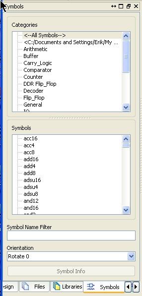
8 Creating a Schematic Your project can be totally Verilog, or totally schematics, or a mixture of the two. This example will feature a mix, just to show you how it can be done. 1. Start by going to Project NewSource and this time choosing schematic as the type. I m calling this fulladd. You can probably guess where this is going 2. In the schematic window you ll see a frame in which you can put your schematic components. You can select components by selecting the Symbols tab in the Sources pane. The first one I like to add is under General Category and is the Title component for the schematic. You can fill in the fields of the Title by double clicking on it. Then I ll add three copies of mynand from my example library, and two copies of the xor2 component from the Logic Category.

9
10

11 3. Now I ll use the wiring tool to connect up the components to make a Full Adder.


12 4. I ll use the I/O Marker tool to add markers on the signals that I d like to export from this circuit. Double click on the I/O Markers to change their names
, and part Verilog (your mynand.v code).")
13 The circuit with the I/O Marker looks like this: 5. Save the schematic. You are now ready to simulate the circuit that consists of part schematics (using xor2 from the Xilinx library), and part Verilog (your mynand.v code). If you go back to the Sources pane and expand the fulladd schematic you will see that it includes three copies of mynand.v.

14 Simulating your Circuit: Now that you have a saved source file (fulladd is the top file in this case), you can simulate its behavior. We ll use the ISE simulator with a testbench to drive the simulation. Note that the testbench files that drive the simulations are also Verilog files. To simulate the fulladd circuit: 1. Go to the top left pane (design) and change the View field to be Simulation. This changes the view to include sources that are interesting for simulation, and also changes the options in the bottom Processes pane to show the simulation options. 2. You can go to the Project NewSource menu again, or you can select the Create New Source widget. This will bring up the New Source Wizard. In that dialog type in the name of your testbench file, and make sure to select Verilog Test Fixture in the list on the left. I will name my testbench fulladd_tb (where the tb stands for testbench). The box looks like:
15 3. The Next dialog asks you which source you want the testbench constructed from. I ll choose fulladd, of course. The code that gets generated includes an instance of the fulladd schematic named UUT (for Unit Under Test).

16 4. Note that the generated template has some code with an ifdef for initializing things. I don t use the ifdef code. Instead I write my own initial block and driving code for testing the circuit. Remember that good testbenches ALWAYS use $display statements and if checks so that the testbench is self-checking! You could enumerate all eight possibilities of the inputs and check the outputs. I m going to get a tiny bit tricky with a concatenation and a loop. 5. Once you fill in the testbench with Verilog code to drive the simulation, you can check the syntax and run the simulation from the Processes tab.

17 The output will be displayed as waveforms, and the $display data will show up in the console as shown (after zooming out to see all the waveforms). You can see that not only do the waveforms show the results of the simulation, but the $display statements have printed data, and because the circuit is correctly functioning, no error statements were printed.

18


19 6. I ll change the circuit to have a mistake to show off my self-checking testbench

20 It s easy to tell that something s wrong!

21 Synthesizing your circuit to the Xilinx FPGA Now that you have a correctly simulating Verilog module, you will have the ISE (webpack) tool synthesize your Verilog to something that can be mapped to the Xilinx FPGA. That is, the Verilog code will be converted by ISE to some gates that are on the FPGA. To be even more specific, ISE will convert the schematic/verilog project description into a set of configuration bits that are used to program the Xilinx part. Those configuration bits are in a.bit file and are downloaded to the Xilinx part in this section of the tutorial. You will use your Spartan-3E board for this part of the tutorial. This is known as the Spartan 3E Starter Kit and is a board produced by Xilinx. It is a very featureladen board with a Spartan 3e XC3S500E FPGA, 64Mbytes of SDRAM, 128Mbits of flash EPROM, A/D and D/A converters, RS232 drivers, VGA, PS/2, USB, and Ethernet connectors, a 16 character two-line LCD, and a lot more. You can get more info from Xilinx at
 Use the impact tools from Xilinx (part of WebPACK) to configure the FPGA through the USB connection. 1.")
22 Specifically we will need to: Assign A, B, and Y to the correct pins on the FPGA that connect to the switches and LEDs on the S3E board Synthesize the Verilog code into FPGA configuration Generate a programming file with all this information (.bit file) Use the impact tools from Xilinx (part of WebPACK) to configure the FPGA through the USB connection. 1. Back in the Design pane, return to the Implementation view and select your fulladd schematic. Now in the bottom (Processes) pane you will see some options including User Constraints, Synthesize, and Implement Design. The first thing we ll do is assign pins using the User Constraints tab. Expand that tab and select the I/O Pin Planning (PlanAhead) Pre- Synthesis choice. This will let us assign our signals to pins on the Xilinx part using the PlanAhead tool. Because we re headed towards putting this on the Xilinx FPGA on the Spartan-3E board, we need to set some constraints. In particular, we need to tell ISE which pins on the Xilinx chip we want A, B, Cin assigned to so that we can access those from switches, and where we want Cout and Sum so we can see those on the LEDs on the Spartan-3E board. This will open a whole new tool called PlanAhead which you can use to set your pin constraints. You may have to agree to add a UCF (Universal Constraints File) file to your project. You should agree to this.


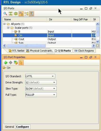
23 2. The PlanAhead tools lets you set a number of different types of constraints on how the circuit is mapped to the Xilinx part. For now we ll just use the pin constraints in the UCF file. You can see a list of the I/O ports from your schematic in the RTL pane (click on the I/I Ports tab in the upper left window). You can set which Xilinx pin they are attached to using the Site field. 3. Clicking on each I/O Port in turn will open the I/O Port Properties pane where you an update the Site field to say which Xilinx pin should be used for that I/O signal.

24 4. How do you know which pins to assign the signals to in order to use the switches and LEDs on the Spartan-3E board? You look in the Spartan-3E Starter Kit Users Manual which is linked to the class web site, and also available from Xilinx at For now I ll just tell you that the four sliding switches on the Spartan-3E board are, from left to right as you re looking at the board with the LCD at the bottom, are on pins N17, H18, L14, and L13. Here s the diagram from the User Guide:


25 and the UCF info is: This tells you how to fill out the information in PlanAhead for the switches. I ll put A, B and Cin on Sw3, Sw2, and Sw1. 5. Note that you ll have to click on Configure in the I/O Port Properties to set some of the parameters to be as specified in the User Guide.
26


27 6. The LEDs are also described in the User Guide: I ll use LED1 and LED0 as Cout and Sum. Note that it s important to get all the details of the pins correct as they re described in the manual! The switches won t function properly without the pullup, for example, and the LEDs really need to have the drive strength set.

28 7. Now Save the PlanAhead settings. This will update things in your main ISE Webpack project. 8. When you exit you ll see that a fulladd.ucf file has been added to the project You can also edit fulladd.ucf by opening it in a text editor. It s just a text file with constraints formatted as shown in the User Guide. The text file looks like this: If you double click on the UCF file you ll see what s in it using the ISE GUI.

29 9. Synthesize XST. Double click on this to synthesize your circuit. After a while you will (hopefully) get the Process Synthesize completed successfully message in the console. If you ve already simulated your circuit and found it to do what you want, there s every chance that this will synthesize correctly without problems. In any case, there is lots of interesting information in the synthesis report (the data in the console window). It s worth looking at, although for this amazingly simple example there isn t anything that fascinating. Make sure that you end the process with a green check for this process. If you get something else, especially a red X, you ll need to fix errors and resynthesize.

. You should see a green check mark if this step finishes without issues.")
30 10. With your source file selected (fulladder in this case), double click the Implement Design process in the Processes tab. This will translate the design to something that can physically be mapped to the particular FPGA that s on our board (the xc3s500e-5fg320 in this case). You should see a green check mark if this step finishes without issues. If there are issues, you need to read them for clues about what went wrong and what you should look at to fix things.

31 11. If you expand this Implement Design tab (which is not necessary) you will see that the Implement Design process actually consists of three parts: a. Translate: Translate is the first step in the implementation process. The Translate process merges all of the input netlists and design constraint information and outputs a Xilinx NGD (Native Generic Database) file. The output NGD file can then be mapped to the targeted FPGA device. b. Map: Mapping is the process of assigning a design s logic elements to the specific physical elements that actually implement logic functions in a device. The Map process creates an NCD (Native Circuit Description) file. The NCD file will be used by the PAR process. c. Place and Route (PAR): PAR uses the NCD file created by the Map process to place and route your design. PAR outputs an NCD file that is used by the bitstream generator (BitGen) to create a (.bit) file. The Bit file (see the next step) is what s used to actually program the FPGA. 12. At this point you can look at the Design Summary to find out all sorts of things about your circuit. One thing that you might want to check is to click on the Pinout Report and check that your signals were correctly assigned to the pins you wanted them to be assigned to.
. 14.")

32 13. Now double click the process: Generate Programming File. This will generate the actual configuration bits into a.bit file that you can use to program your Spartan-3E board to behave like your circuit (in this case a full adder). 14. Now that you have the programming file, you can program the Spartan-3E board using the impact tool and the USB cable on your PC/laptop. First, make sure that the jumpers on your Spartan-3E board are installed correctly. In particular, check that the configuration options are correctly set. The configuration options are at the top of the board near the RS232 interfaces.


33 The jumpers on the J30 headers must be set for JTAG programming. This means that only the middle pins of the header should have a jumper on them. See the following illustration from the User Guide. Your board should look like this! 15. Now that you have the jumpers set correctly, you can plug in the power to your Spartan-3E board, and connect the USB cable between the Spartan- 3E and your PC. Then when you turn on the power, the PC should


34 recognize the Xilinx cable/board and install the drivers. 16. Once the PC has recognized the USB connection to the Spartan-3E board, you can use the Process Configure Target Device to start up the impact tool to program the FPGA. 17. The first time you Configure Target Device for a new project, you ll get the following message about setting up an impact file. You can click OK here and start up the impact tool. 18. You ll now get yet another tool the impact device configuration and programming tool:

35 19. Double-click the Boundary Scan button to configure the Xilinx part for programming. Boundary Scan is the technique that is used on these devices for uploading the bit file to the Xilinx part through the USB cable. You will be prompted to Right Click to Add Device or Initialize JTAG Chain. JTAG is the acronym for the boundary scan standard that is used for programming in this case. When you right-click you get a menu. What Select Initialize Chain. There are actually three programmable parts on the Spartan3 board and they are organized in a chain passing the bits from one device to the other. This is the chain that is being initialized.

 or each of the programmable chips on the Spartan-3E board.")
36 Note that you MUST have your board plugged in to the USB cable and turned on for this step! The initialization procedure sends a query out on the USB cable to see what chips are out there. If you have everything plugged in and turned on it will see the chips and initialize the chain. You should continue and assign a configuration file: 20. You will now be asked to choose a configuration file (which will be a.bit file) or each of the programmable chips on the Spartan-3E board. Note that there are three of them, but the xc3s500e is the only one you should program. The other two are already programmed with supporting tasks on the board. Choose the file that you want programmed into the FPGA. In this case that s fulladd.bit.

, or to bypass. You should choose bypass for the other chips (the xcf04s and the xc2c64).")
37 You will also be asked if you want to attach an SPI or BPI PROM to the device. For now you should say No. There is a 16Mbit SPI PROM attached to the Xilinx part and later on you may want to include a PROM data file here so that the bitstream will also load that prom. For each of the other chips you can choose to open a file (attach a.bit file to that chip), or to bypass. You should choose bypass for the other chips (the xcf04s and the xc2c64). The summary looks like this:

38 21. In the impact screen you should now see the following window that shows the programmable chips and the associated bit files or bypass configurations.

39 22. Now you can select the Spartan-3E (the xc3s500e) and right click to get a dialog. Select Program in this dialog to program the FPGA. You should see the following indication that the programming has succeeded. You should also see the xc-done LED (a little yellow LED underneath the J30 jumper on the board) light up if the programming is successful. 23. Your circuit should now be running on the Spartan-3E board. If you ve followed this tutorial you should now be able to set the sw3, sw2, and sw1 switches and look for the full adder output on LDE1 and LED If you make changes and want to reload the bit file to the FPGA (after making changes, for example), you can restart the impact tool using the Manage Configuration Project (impact) option under Configure Target Device.


40 You can then right click on the xc3s500e device and program it with the new bit file or use the impact Processes in the lower left: Whew! That s it
41 Overview of the Procedure 1. Design the circuit that you would like to map to the Xilinx part on the FPGA. You can use schematics, or Verilog, or a mixture of both. 2. Simulate your circuit using the ISE Simulator and a Verilog testbench to provide inputs to the circuit. Use if statements in your testbench to make it self-checking. 3. Generate a UCF file to hold constraints such as pin assignments (later we ll use the UCF file for other constraints like timing and speed). Use the PlanAhead tool to generate this file. 4. Assign the I/O pins in your design to the pins on the FPGA that you want them connected to. 5. Synthesize the design for the FPGA using the XST synthesis tool. 6. Implement the design to map it to the specific FPGA on the Spartan-3E board 7. Generate the programming.bit file that has the bitstream that configures the FPGA. 8. Connect your Spartan3 board to the computer and use theimpact tool to program the FPGA using the bitstream. \
Tutorial: Working with Verilog and the Xilinx FPGA in ISE 9.2i
 Tutorial: Working with Verilog and the Xilinx FPGA in ISE 9.2i This tutorial will show you how to: Use Verilog to specify a design Simulate that Verilog design Define pin constraints for the FPGA (.ucf
and 32 bit for 32 bit. If you don t pay attention to this, there will be unexpected behavior in the ISE software and thing may not work properly!
 This tutorial will show you how to: Part I: Set up a new project in ISE 14.7 Part II: Implement a function using Schematics Part III: Simulate the schematic circuit using ISim Part IV: Constraint, Synthesize,
Tutorial: Working with the Xilinx tools 14.4
 Tutorial: Working with the Xilinx tools 14.4 This tutorial will show you how to: Part I: Set up a new project in ISE Part II: Implement a function using Schematics Part III: Implement a function using
TLL5000 Electronic System Design Base Module. Getting Started Guide, Ver 3.4
 TLL5000 Electronic System Design Base Module Getting Started Guide, Ver 3.4 COPYRIGHT NOTICE The Learning Labs, Inc. ( TLL ) All rights reserved, 2008 Reproduction in any form without permission is prohibited.
Banks, Jasmine Elizabeth (2011) The Spartan 3E Tutorial 1 : Introduction to FPGA Programming, Version 1.0. [Tutorial Programme]
![Banks, Jasmine Elizabeth (2011) The Spartan 3E Tutorial 1 : Introduction to FPGA Programming, Version 1.0. [Tutorial Programme]](/thumbs/75/72381729.jpg "Banks, Jasmine Elizabeth (2011) The Spartan 3E Tutorial 1 : Introduction to FPGA Programming, Version 1.0. [Tutorial Programme]") QUT Digital Repository: http://eprints.qut.edu.au/ This is the author version published as: This is the accepted version of this article. To be published as : This is the author s version published as:
QUT Digital Repository: http://eprints.qut.edu.au/ This is the author version published as: This is the accepted version of this article. To be published as : This is the author s version published as:
Xilinx ISE Synthesis Tutorial
 Xilinx ISE Synthesis Tutorial The following tutorial provides a basic description of how to use Xilinx ISE to create a simple 2-input AND gate and synthesize the design onto the Spartan-3E Starter Board
Introduction. About this tutorial. How to use this tutorial
 Basic Entry & not About this tutorial This tutorial consists of an introduction to creating simple circuits on an FPGA using a variety of methods. There are two ways to create the circuit: using or by
4. Verify that HDL is selected as the Top-Level Source Type, and click Next. The New Project Wizard Device Properties page appears.
 Working with the GODIL Author: Ruud Baltissen Credits: Michael Randelzhofer, Ed Spittles Date: August 2010 What is it? This document describes a way to get familiar with the Xilinx FPGAs on OHO s Godil,
TLL5000 Electronic System Design Base Module
 TLL5000 Electronic System Design Base Module The Learning Labs, Inc. Copyright 2007 Manual Revision 2007.12.28 1 Copyright 2007 The Learning Labs, Inc. Copyright Notice The Learning Labs, Inc. ( TLL )
ECE 491 Laboratory 1 Introducing FPGA Design with Verilog September 6, 2004
 Goals ECE 491 Laboratory 1 Introducing FPGA Design with Verilog September 6, 2004 1. To review the use of Verilog for combinational logic design. 2. To become familiar with using the Xilinx ISE software
Xilinx ISE8.1 and Spartan-3 Tutorial EE3810
 Xilinx ISE8.1 and Spartan-3 Tutorial EE3810 1 Part1) Starting a new project Simple 3-to-8 Decoder Start the Xilinx ISE 8.1i Project Navigator: Select File > New Project in the opened window 2 Select a
Xilinx ISE8.1 and Spartan-3 Tutorial (Prepared by Kahraman Akdemir based on Professor Duckworth's Tutorials updated September 2006)
") Xilinx ISE8.1 and Spartan-3 Tutorial (Prepared by Kahraman Akdemir based on Professor Duckworth's Tutorials updated September 2006) 1 Part1) Starting a new project Simple 3-to-8 Decoder Start the Xilinx
Xilinx ISE8.1 and Spartan-3 Tutorial (Prepared by Kahraman Akdemir based on Professor Duckworth's Tutorials updated September 2006) 1 Part1) Starting a new project Simple 3-to-8 Decoder Start the Xilinx
Programming Xilinx SPARTAN 3 Board (Simulation through Implementation)
") Programming Xilinx SPARTAN 3 Board (Simulation through Implementation) September 2008 Prepared by: Oluwayomi Adamo Class: Project IV University of North Texas FPGA Physical Description 4 1. VGA (HD-15)
Programming Xilinx SPARTAN 3 Board (Simulation through Implementation) September 2008 Prepared by: Oluwayomi Adamo Class: Project IV University of North Texas FPGA Physical Description 4 1. VGA (HD-15)
EE 1315 DIGITAL LOGIC LAB EE Dept, UMD
 EE 1315 DIGITAL LOGIC LAB EE Dept, UMD EXPERIMENT # 1: Logic building blocks The main objective of this experiment is to let you familiarize with the lab equipment and learn about the operation of the
Nexys 2/3 board tutorial (Decoder, ISE 13.2) Jim Duckworth, August 2011, WPI. (updated March 2012 to include Nexys2 board)
 Jim Duckworth, August 2011, WPI. (updated March 2012 to include Nexys2 board)") Nexys 2/3 board tutorial (Decoder, ISE 13.2) Jim Duckworth, August 2011, WPI. (updated March 2012 to include Nexys2 board) Note: you will need the Xilinx ISE Webpack installed on your computer (or you
Nexys 2/3 board tutorial (Decoder, ISE 13.2) Jim Duckworth, August 2011, WPI. (updated March 2012 to include Nexys2 board) Note: you will need the Xilinx ISE Webpack installed on your computer (or you
Building Combinatorial Circuit Using Behavioral Modeling Lab
 Building Combinatorial Circuit Using Behavioral Modeling Lab Overview: In this lab you will learn how to model a combinatorial circuit using behavioral modeling style of Verilog HDL. You will model a combinatorial
Circuit design with configurable devices (FPGA)
") 1 Material Circuit design with configurable devices (FPGA) Computer with Xilinx's ISE software installed. Digilent's Basys2 prototype board and documentation. Sample design files (lab kit). Files and documents
1 Material Circuit design with configurable devices (FPGA) Computer with Xilinx's ISE software installed. Digilent's Basys2 prototype board and documentation. Sample design files (lab kit). Files and documents
Xilinx Tutorial Basic Walk-through
 Introduction to Digital Logic Design with FPGA s: Digital logic circuits form the basis of all digital electronic devices. FPGAs (Field Programmable Gate Array) are large programmable digital electronic
Using Synplify Pro, ISE and ModelSim
 Using Synplify Pro, ISE and ModelSim VLSI Systems on Chip ET4 351 Rene van Leuken Huib Lincklaen Arriëns Rev. 1.2 The EDA programs that will be used are: For RTL synthesis: Synplicity Synplify Pro For
FPGA Design Flow 1. All About FPGA
 FPGA Design Flow 1 In this part of tutorial we are going to have a short intro on FPGA design flow. A simplified version of FPGA design flow is given in the flowing diagram. FPGA Design Flow 2 FPGA_Design_FLOW
Lab 6: Intro to FPGAs
 Lab 6: Intro to FPGAs UC Davis Physics 116B Rev 2/22/2018 There s a saying when dealing with complex electronic systems: If you can make the LED blink, you re 90% of the way there., so in this lab you
Getting Started with Xilinx WebPack 13.1
 Getting Started with Xilinx WebPack 13.1 B. Ackland June 2011 (Adapted from S. Tewksbury notes WebPack 7.1) This tutorial is designed to help you to become familiar with the operation of the WebPack software
Department of Electrical and Computer Engineering Xilinx ISIM <Release Version: 14.1i> Simulation Tutorial Using Verilog
 Department of Electrical and Computer Engineering Xilinx ISIM Simulation Tutorial Using Verilog Spring 2013 Baback Izadi You will next test the full adder circuit that you built
ECE 4305 Computer Architecture Lab #1
 ECE 4305 Computer Architecture Lab #1 The objective of this lab is for students to familiarize with the FPGA prototyping system board (Nexys-2) and the Xilinx software development environment that will
The board is powered by the USB connection, so to turn it on or off you plug it in or unplug it, respectively.
 Lab 1 You may work in pairs or individually on this lab Lab Objectives Learn about the equipment we will be using and how to handle it safely. Learn the basics of using Xilinx ISE to develop hardware designs
Implementing a Verilog design into the UWEE CPLD Development Board Using Xilinx s ISE 7.1i Software: A Tutorial
 Implementing a Verilog design into the UWEE CPLD Development Board Using Xilinx s ISE 7.1i Software: A Tutorial Revision 0 By: Evan Gander Materials: The following are required in order to complete this
CECS LAB 1 Introduction to Xilinx EDA Tools
 NAME: DUE DATE: STUDENT ID: POSSIBLE POINTS: 10 COURSE DATE & TIME: OBJECTIVE: To familiarize ourselves with the Xilinx Electronic Design Aid (EDA) Tools. We will simulate a simple 4-to-1 Multiplexor using
ISE Design Suite Software Manuals and Help
 ISE Design Suite Software Manuals and Help These documents support the Xilinx ISE Design Suite. Click a document title on the left to view a document, or click a design step in the following figure to
E85: Digital Design and Computer Engineering Lab 2: FPGA Tools and Combinatorial Logic Design
 E85: Digital Design and Computer Engineering Lab 2: FPGA Tools and Combinatorial Logic Design Objective The purpose of this lab is to learn to use Field Programmable Gate Array (FPGA) tools to simulate
NOTE: This tutorial contains many large illustrations. Page breaks have been added to keep images on the same page as the step that they represent.
 CSE 352 Tutorial # 4 Synthesizing onto an FPGA Objectives This tutorial will walk you through the steps of implementing a design made in Active-HDL onto the Altera Cyclone II FPGA NOTE: This tutorial contains
Revision: February 27, E Main Suite D Pullman, WA (509) Voice and Fax
 Voice and Fax") Xilinx ISE WebPACK Schematic Capture Tutorial Revision: February 27, 2010 215 E Main Suite D Pullman, WA 99163 (509) 334 6306 Voice and Fax Overview This tutorial provides instruction for using the Xilinx
Xilinx ISE WebPACK Schematic Capture Tutorial Revision: February 27, 2010 215 E Main Suite D Pullman, WA 99163 (509) 334 6306 Voice and Fax Overview This tutorial provides instruction for using the Xilinx
University of Hawaii EE 361L. Getting Started with Spartan 3E Digilent Basys2 Board. Lab 4.1
 University of Hawaii EE 361L Getting Started with Spartan 3E Digilent Basys2 Board Lab 4.1 I. Test Basys2 Board Attach the Basys2 board to the PC or laptop with the USB connector. Make sure the blue jumper
Chip Design with FPGA Design Tools
 Chip Design with FPGA Design Tools Intern: Supervisor: Antoine Vazquez Janusz Zalewski Florida Gulf Coast University Fort Myers, FL 33928 V1.9, August 28 th. Page 1 1. Introduction FPGA is abbreviation
Board-Data Processing. VHDL Exercises. Exercise 1: Basics of VHDL Programming. Stages of the Development process using FPGA s in Xilinx ISE.
 Board-Data Processing VHDL Exercises Exercise 1: Basics of VHDL Programming Stages of the Development process using FPGA s in Xilinx ISE. Basics of VHDL VHDL (Very High Speed IC Hardware description Language)
ENGN3213. Digital Systems & Microprocessors. CLAB 1: ICARUS Verilog and ISE WebPACK
 Department of Engineering Australian National University ENGN3213 Digital Systems & Microprocessors CLAB 1: ICARUS Verilog and ISE WebPACK V3.0 Copyright 2010 G.G. Borg ANU Engineering 1 Contents 1 CLAB1:
EE 367 Logic Design Lab #1 Introduction to Xilinx ISE and the ML40X Eval Board Date: 1/21/09 Due: 1/28/09
 EE 367 Logic Design Lab #1 Introduction to Xilinx ISE and the ML40X Eval Board Date: 1/21/09 Due: 1/28/09 Lab Description Today s lab will introduce you to the Xilinx Integrated Software Environment (ISE)
Lab 1: Introduction to Verilog HDL and the Xilinx ISE
 EE 231-1 - Fall 2016 Lab 1: Introduction to Verilog HDL and the Xilinx ISE Introduction In this lab simple circuits will be designed by programming the field-programmable gate array (FPGA). At the end
CS/EE Prerequsites. Hardware Infrastructure. Class Goal CS/EE Computer Design Lab. Computer Design Lab Fall 2010
 CS/EE 3710 Computer Design Lab Fall 2010 CS/EE 3710 Computer Design Lab T Th 3:40pm-5:00pm Lectures in WEB 110, Labs in MEB 3133 (DSL) Instructor: Erik Brunvand MEB 3142 Office Hours: After class, when
CS/EE Computer Design Lab Fall 2010 CS/EE T Th 3:40pm-5:00pm Lectures in WEB 110, Labs in MEB 3133 (DSL) Instructor: Erik Brunvand
 Instructor: Erik Brunvand") CS/EE 3710 Computer Design Lab Fall 2010 CS/EE 3710 Computer Design Lab T Th 3:40pm-5:00pm Lectures in WEB 110, Labs in MEB 3133 (DSL) Instructor: Erik Brunvand MEB 3142 Office Hours: After class, when
CS/EE 3710 Computer Design Lab Fall 2010 CS/EE 3710 Computer Design Lab T Th 3:40pm-5:00pm Lectures in WEB 110, Labs in MEB 3133 (DSL) Instructor: Erik Brunvand MEB 3142 Office Hours: After class, when
CS152 FPGA CAD Tool Flow University of California at Berkeley College of Engineering Department of Electrical Engineering and Computer Sciences
 CS152 FPGA CAD Tool Flow University of California at Berkeley College of Engineering Department of Electrical Engineering and Computer Sciences Compiled: 4/3/2003 for CS152 Spring 03, Prof. John Kubiatowicz
Verilog Design Entry, Synthesis, and Behavioral Simulation
 ------------------------------------------------------------- PURPOSE - This lab will present a brief overview of a typical design flow and then will start to walk you through some typical tasks and familiarize
To practice combinational logic on Logisim and Xilinx ISE tools. ...
 ENGG1203: Introduction to Electrical and Electronic Engineering Second Semester, 2017 18 Lab 1 Objective: To practice combinational logic on Logisim and Xilinx ISE tools. 1 Find your lab partner You will
Getting started with the Xilinx Project Navigator and the Digilent BASYS 2 board.
 Getting started with the Xilinx Project Navigator and the Digilent BASYS 2 board. This lab is based on: Xilinx Project Navigator, Release Version 14.6 Digilent Adept System Rev 2.7, Runtime Rev 2.16 Digilent
Xilinx Schematic Entry Tutorial
 Overview Xilinx Schematic Entry Tutorial Xilinx ISE Schematic Entry & Modelsim Simulation What is circuit simulation and why is it important? Complex designs, short design cycle Simultaneous system design
Tutorial on FPGA Design Flow based on Xilinx ISE WebPack and ModelSim. ver. 2.0
 Tutorial on FPGA Design Flow based on Xilinx ISE WebPack and ModelSim ver. 2.0 Updated: Fall 2013 1 Preparing the Input: Download examples associated with this tutorial posted at http://ece.gmu.edu/tutorials-and-lab-manuals
After opening the Programs> Xilinx ISE 8.2i > Project Navigator, you will come to this screen as start-up.
 After opening the Programs> Xilinx ISE 8.2i > Project Navigator, you will come to this screen as start-up. Start with a new project. Enter a project name and be sure to select Schematic as the Top-Level
Logic Implementation on a Xilinx FPGA using VHDL WWU Linux platform assumed. rev 10/25/16
 1 Logic Implementation on a Xilinx FPGA using VHDL WWU Linux platform assumed. rev 10/25/16 The following is a general outline of steps (i.e. design flow) used to implement a digital system described with
COS/ELE 375 Verilog & Design Tools Tutorial
 COS/ELE 375 Verilog & Design Tools Tutorial In this tutorial, you will walk through a tutorial using the Xilinx ISE design software with a Digilent Nexys4 DDR FPGA board. In this tutorial, you will learn
Step 1: Downloading the source files
 Introduction: In this lab and in the remainder of the ELEC 2607 labs, you will be using the Xilinx ISE to enter and simulate the designs for your circuits. In labs 3 and 4, you will use ISE to compile
CPEN 230L: Introduction to Digital Logic Laboratory Lab #6: Verilog and ModelSim
 CPEN 230L: Introduction to Digital Logic Laboratory Lab #6: Verilog and ModelSim Purpose Define logic expressions in Verilog using register transfer level (RTL) and structural models. Use Quartus II to
Tutorial on FPGA Design Flow based on Xilinx ISE Webpack and ModelSim. ver. 1.5
 Tutorial on FPGA Design Flow based on Xilinx ISE Webpack and ModelSim ver. 1.5 1 Prepared by Marcin Rogawski, Ekawat (Ice) Homsirikamol, Kishore Kumar Surapathi and Dr. Kris Gaj The example codes used
Experiment 3. Digital Circuit Prototyping Using FPGAs
 Experiment 3. Digital Circuit Prototyping Using FPGAs Masud ul Hasan Muhammad Elrabaa Ahmad Khayyat Version 151, 11 September 2015 Table of Contents 1. Objectives 2. Materials Required 3. Background 3.1.
Xilinx ISE/WebPack: Introduction to Schematic Capture and Simulation
 Xilinx ISE/WebPack: Introduction to Schematic Capture and Simulation Revision: February 7, 2003 Overview This document is intended to assist new entry-level users of the Xilinx ISE/WebPack software. It
ENGN 1630: CPLD Simulation Fall ENGN 1630 Fall Simulating XC9572XLs on the ENGN1630 CPLD-II Board Using Xilinx ISim
 ENGN 1630 Fall 2018 Simulating XC9572XLs on the ENGN1630 CPLD-II Board Using Xilinx ISim You will use the Xilinx ISim simulation software for the required timing simulation of the XC9572XL CPLD programmable
EE183 LAB TUTORIAL. Introduction. Projects. Design Entry
 EE183 LAB TUTORIAL Introduction You will be using several CAD tools to implement your designs in EE183. The purpose of this lab tutorial is to introduce you to the tools that you will be using, Xilinx
Xilinx Project Navigator Reference Guide
 31 July 2003 Author: David M. Sendek Xilinx Project Navigator Reference Guide Background: This guide provides you with step-by-step procedures in using the Xilinx Project Navigator to perform the following:
Introduction to WebPACK 6.3. Using Xilinx WebPACK Software to Create FPGA Designs for the XSA Board
 Introduction to WebPACK 6.3 Using Xilinx WebPACK Software to Create FPGA Designs for the XSA Board Release date: 1/1/2005 2005 by XESS Corp. All XS-prefix product designations are trademarks of XESS Corp.
Logic Implementation on a Xilinx FPGA using VHDL WWU Linux platform assumed. rev 11/01/17
 1 Logic Implementation on a Xilinx FPGA using VHDL WWU Linux platform assumed. rev 11/01/17 The following is a general outline of steps (i.e. design flow) used to implement a digital system described with
Nexys 2 board tutorial (Decoder, ISE 12.2) Jim Duckworth, August 2010, WPI. Digilent Adept Programming Steps added by Zoe (Zhu Fu)
 Jim Duckworth, August 2010, WPI. Digilent Adept Programming Steps added by Zoe (Zhu Fu)") Nexys 2 board tutorial (Decoder, ISE 12.2) Jim Duckworth, August 2010, WPI. Digilent Adept Programming Steps added by Zoe (Zhu Fu) Note: you will need the Xlinx ISE Webpack installed on your compuer (or
Nexys 2 board tutorial (Decoder, ISE 12.2) Jim Duckworth, August 2010, WPI. Digilent Adept Programming Steps added by Zoe (Zhu Fu) Note: you will need the Xlinx ISE Webpack installed on your compuer (or
ELEC 4200 Lab#0 Tutorial
 1 ELEC 4200 Lab#0 Tutorial Objectives(1) In this Lab exercise, we will design and implement a 2-to-1 multiplexer (MUX), using Xilinx Vivado tools to create a VHDL model of the design, verify the model,
1 Discussion. 2 Pre-Lab
 CSE 275 Digital Design Lab Lab 3 Implementation of a Combinational Logic Circuit Penn State Erie, The Behrend College Fall Semester 2007 Number of Lab Periods: 1 1 Discussion The purpose of this lab is
Introduction to WebPACK 6.1. Using Xilinx WebPACK Software to Create FPGA Designs for the XSA Board
 Introduction to WebPACK 6.1 Using Xilinx WebPACK Software to Create FPGA Designs for the XSA Board Release date: 10/30/2003 All XS-prefix product designations are trademarks of XESS Corp. All XC-prefix
ANADOLU UNIVERSITY DEPARTMENT OF ELECTRICAL AND ELECTRONICS ENGINEERING. EEM Digital Systems II
 ANADOLU UNIVERSITY DEPARTMENT OF ELECTRICAL AND ELECTRONICS ENGINEERING EEM 334 - Digital Systems II LAB 1 - INTRODUCTION TO XILINX ISE SOFTWARE AND FPGA 1. PURPOSE In this lab, after you learn to use
Tutorial on FPGA Design Flow based on Xilinx ISE Webpack andisim. ver. 1.0
 Tutorial on FPGA Design Flow based on Xilinx ISE Webpack andisim ver. 1.0 1 Prepared by Malik Umar Sharif and Dr. Kris Gaj The example codes used in this tutorial can be obtained from http://ece.gmu.edu/coursewebpages/ece/ece448/s11/labs/448_lab3.htm
Tutorial on FPGA Design Flow based on Aldec Active HDL. Ver 1.5
 Tutorial on FPGA Design Flow based on Aldec Active HDL Ver 1.5 1 Prepared by Ekawat (Ice) Homsirikamol, Marcin Rogawski, Jeremy Kelly, John Pham, and Dr. Kris Gaj This tutorial assumes that you have basic
Revision: February 27, E Main Suite D Pullman, WA (509) Voice and Fax
 Voice and Fax") Xilinx ISE WebPACK VHDL Tutorial Revision: February 27, 2010 215 E Main Suite D Pullman, WA 99163 (509) 334 6306 Voice and Fax Overview This tutorial provides simple instruction for using the Xilinx ISE
Xilinx ISE WebPACK VHDL Tutorial Revision: February 27, 2010 215 E Main Suite D Pullman, WA 99163 (509) 334 6306 Voice and Fax Overview This tutorial provides simple instruction for using the Xilinx ISE
XILINX ISE AND SPARTAN 3AN TUTORIAL
 XILINX ISE AND SPARTAN 3AN TUTORIAL SYNTETIZE AND SIMULATION------------------------------------------ This tutorial will show you how to create a simple Xilinx ISE project based on the Spartan-3 Board.
Introduction to WebPACK 5.2 for FPGAs. Using Xilinx WebPACK Software to Create FPGA Designs for the XSB-300E Board
 Introduction to WebPACK 5.2 for FPGAs Using Xilinx WebPACK Software to Create FPGA Designs for the XSB-300E Board Release date: 10/27/2003 All XS-prefix product designations are trademarks of XESS Corp.
Introduction to WebPACK 8.1. Using Xilinx WebPACK Software to Create FPGA Designs for the XSA Board
 Introduction to WebPACK 8.1 Using Xilinx WebPACK Software to Create FPGA Designs for the XSA Board Release date: 5/16/2005 2006 by XESS Corp. All XS-prefix product designations are trademarks of XESS
OVERVIEW OF FPGA AND EDA SOFTWARE
 CHAPTER 2 OVERVIEW OF FPGA AND EDA SOFTWARE 2.1 INTRODUCTION Developing a large FPGA-based system is an involved process that consists of many complex transformations and optimization algorithms. Software
Xilinx ISE Simulation Tutorial
 Xilinx ISE Simulation Tutorial 1. Start Xilinx ISE Project Navigator 2. Create a new project Click on File, then choose New Project on the drop down menu Enter your project name, in this case the project
Programmable Logic Design I
 Programmable Logic Design I Introduction In labs 11 and 12 you built simple logic circuits on breadboards using TTL logic circuits on 7400 series chips. This process is simple and easy for small circuits.
Guide ISE14. ISE 14.2 (Xilinx) Designflow 1/12
 Designflow 1/12") Guide ISE14 ISE 14.2 (Xilinx) Designflow 1/12 Inhaltsverzeichnis 1. Create a Project 3 2. Select a Device 4 3. Add the Sourcecodes 5 4. File for the Pinning 6 5. Synthesis 7 6. Implementation 8 7. Programming
Guide ISE14 ISE 14.2 (Xilinx) Designflow 1/12 Inhaltsverzeichnis 1. Create a Project 3 2. Select a Device 4 3. Add the Sourcecodes 5 4. File for the Pinning 6 5. Synthesis 7 6. Implementation 8 7. Programming
CSE P567 - Winter 2010 Lab 1 Introduction to FGPA CAD Tools
 CSE P567 - Winter 2010 Lab 1 Introduction to FGPA CAD Tools This is a tutorial introduction to the process of designing circuits using a set of modern design tools. While the tools we will be using (Altera
Using XILINX WebPACK Software to Create CPLD Designs
 Introduction to WebPACK Using XILINX WebPACK Software to Create CPLD Designs RELEASE DATE: 10/24/1999 All XS-prefix product designations are trademarks of XESS Corp. All XC-prefix product designations
Quartus II Tutorial. September 10, 2014 Quartus II Version 14.0
 Quartus II Tutorial September 10, 2014 Quartus II Version 14.0 This tutorial will walk you through the process of developing circuit designs within Quartus II, simulating with Modelsim, and downloading
Introduction to WebPACK 4.1 for FPGAs. Using Xilinx WebPACK Software to Create FPGA Designs for the XSA Board
 Introduction to WebPACK 4.1 for FPGAs Using Xilinx WebPACK Software to Create FPGA Designs for the XSA Board Release date: 10/29/2001 All XS-prefix product designations are trademarks of XESS Corp. All
LAB #3: ADDERS and COMPARATORS using 3 types of Verilog Modeling
 LAB #3: ADDERS and COMPARATORS using 3 types of Verilog Modeling LAB OBJECTIVES 1. Practice designing more combinational logic circuits 2. More experience with equations and the use of K-maps and Boolean
Tutorial on FPGA Design Flow based on Xilinx ISE Webpack and ModelSim. ver. 1.3
 Tutorial on FPGA Design Flow based on Xilinx ISE Webpack and ModelSim ver. 1.3 1 Prepared by Marcin Rogawski, Ekawat (Ice) Homsirikamol, Kishorekum Surapathi, and Dr. Kris Gaj The example codes used in
The UNIVERSITY of NORTH CAROLINA at CHAPEL HILL
 The UNIVERSITY of NORTH CAROLINA at CHAPEL HILL Comp 541 Digital Logic and Computer Design Spring 2015 Lab #1: Getting Started Issued Fri. 1/9/15; Due Wed. 1/14/15 (11:59pm) This lab assignment consists
Quartus II Version 14.0 Tutorial Created September 10, 2014; Last Updated January 9, 2017
 Quartus II Version 14.0 Tutorial Created September 10, 2014; Last Updated January 9, 2017 This tutorial will walk you through the process of developing circuit designs within Quartus II, simulating with
Engineering 1630 Fall Simulating XC9572XL s on the ENGN1630 CPLD-II Board
 Engineering 1630 Fall 2016 Simulating XC9572XL s on the ENGN1630 CPLD-II Board You will use the Aldec Active-HDL software for the required timing simulation of the XC9572XL CPLD programmable logic chips
Configuring the Xilinx Spartan-6 LX9 MicroBoard
 Configuring the Xilinx Spartan-6 LX9 MicroBoard Version 1.3 Table of Contents Table of Contents... 2 Table of Figures... 3 Revision History... 4 Overview... 5 Configuration and Programming via the on-board
SP601 MultiBoot Design
 SP601 MultiBoot Design December 2009 Copyright 2009 Xilinx XTP038 Note: This presentation applies to the SP601 Overview Spartan-6 MultiBoot Capability Xilinx SP601 Board Software Requirements SP601 Setup
Digital Circuit Design Using Xilinx ISE Tools
 Digital Circuit Design Using Xilinx ISE Tools Poras T. Balsara and Prashant Vallur Table of Contents 1. Introduction 2. Programmable logic devices: FPGA and CPLD 3. Creating a new project in Xilinx Foundation
Tutorial on Quartus II Introduction Using Verilog Code
 Tutorial on Quartus II Introduction Using Verilog Code (Version 15) 1 Introduction This tutorial presents an introduction to the Quartus II CAD system. It gives a general overview of a typical CAD flow
Vivado Walkthrough ECGR Fall 2015
 ECGR 2181 - Vivado Walkthrough 1 Vivado Walkthrough ECGR 2181 - Fall 2015 Intro In this walkthrough we re going to go through the process of creating a project, adding sources, writing vhdl, simulating
Design a three-input, two-output sequential digital circuit which functions as a digital locking mechanism. LOCK ALARM
 Department of Computing Course 112 Hardware First Year Laboratory Assignment Dates for the session 2005-2006: Hand out Date: 10 th January 2006 Hand in deadline (electronic and written report): 17.00 Monday
AccelDSP tutorial 2 (Matlab.m to HDL for Xilinx) Ronak Gandhi Syracuse University Fall
 Ronak Gandhi Syracuse University Fall") AccelDSP tutorial 2 (Matlab.m to HDL for Xilinx) Ronak Gandhi Syracuse University Fall 2009-10 AccelDSP Getting Started Tutorial Introduction This tutorial exercise will guide you through the process of
AccelDSP tutorial 2 (Matlab.m to HDL for Xilinx) Ronak Gandhi Syracuse University Fall 2009-10 AccelDSP Getting Started Tutorial Introduction This tutorial exercise will guide you through the process of
ECT 224: Digital Computer Fundamentals Using Xilinx StateCAD
 ECT 224: Digital Computer Fundamentals Using Xilinx StateCAD 1) Sequential circuit design often starts with a problem statement tat can be realized in the form of a state diagram or state table a) Xilinx
Tutorial on FPGA Design Flow based on Aldec Active HDL. ver 1.7
 Tutorial on FPGA Design Flow based on Aldec Active HDL ver 1.7 Fall 2012 1 Prepared by Ekawat (Ice) Homsirikamol, Marcin Rogawski, Jeremy Kelly, Kishore Kumar Surapathi, Ambarish Vyas, Malik Umar Sharif
FPGA Design Flow. - from HDL to physical implementation - Victor Andrei. Kirchhoff-Institut für Physik (KIP) Ruprecht-Karls-Universität Heidelberg
 Ruprecht-Karls-Universität Heidelberg") FPGA Design Flow - from HDL to physical implementation - Victor Andrei Kirchhoff-Institut für Physik (KIP) Ruprecht-Karls-Universität Heidelberg 6th Detector Workshop of the Helmholtz Alliance Physics
FPGA Design Flow - from HDL to physical implementation - Victor Andrei Kirchhoff-Institut für Physik (KIP) Ruprecht-Karls-Universität Heidelberg 6th Detector Workshop of the Helmholtz Alliance Physics
1. Downloading. 2. Installation and License Acquiring. Xilinx ISE Webpack + Project Setup Instructions
 Xilinx ISE Webpack + Project Setup Instructions 1. Downloading The Xilinx tools are free for download from their website and can be installed on your Windowsbased PC s. Go to the following URL: http://www.xilinx.com/support/download/index.htm
Digital Electronics & Computer Engineering (E85)
") Digital Electronics & Computer Engineering (E85) Lab 4: Thunderbird Turn Signal Introduction In this lab, you will design a finite state machine to control the taillights of a 1965 Ford Thunderbird 1 and
Digital Electronics & Computer Engineering (E85) Lab 4: Thunderbird Turn Signal Introduction In this lab, you will design a finite state machine to control the taillights of a 1965 Ford Thunderbird 1 and
Circuit Design and Simulation with VHDL 2nd edition Volnei A. Pedroni MIT Press, 2010 Book web:
 Circuit Design and Simulation with VHDL 2nd edition Volnei A. Pedroni MIT Press, 2010 Book web: www.vhdl.us Appendix C Xilinx ISE Tutorial (ISE 11.1) This tutorial is based on ISE 11.1 WebPack (free at
Chapter 9: Integration of Full ASIP and its FPGA Implementation
 Chapter 9: Integration of Full ASIP and its FPGA Implementation 9.1 Introduction A top-level module has been created for the ASIP in VHDL in which all the blocks have been instantiated at the Register
Tutorial on FPGA Design Flow based on Aldec Active HDL. Ver 1.5
 Tutorial on FPGA Design Flow based on Aldec Active HDL Ver 1.5 1 Prepared by Ekawat (Ice) Homsirikamol, Marcin Rogawski, Jeremy Kelly, Kishore Kumar Surapathi and Dr. Kris Gaj This tutorial assumes that
Lab 3: Xilinx PicoBlaze Flow Lab Targeting Spartan-3E Starter Kit
 Lab 3: Xilinx PicoBlaze Flow Lab Targeting Spartan-3E Starter Kit Xilinx PicoBlaze Flow Demo Lab www.xilinx.com 1-1 Create a New Project Step 1 Create a new project targeting the Spartan-3E device that
CCE 3202 Advanced Digital System Design
 CCE 3202 Advanced Digital System Design Lab Exercise #2 Introduction You will use Xilinx Webpack v9.1 to allow the synthesis and creation of VHDLbased designs. This lab will outline the steps necessary
CPE 200L LABORATORY 4: INTRODUCTION TO DE2 BOARD UNIVERSITY OF NEVADA, LAS VEGAS GOALS: BACKGROUND:
 CPE 200L LABORATORY 4: INTRODUCTION TO DE2 BOARD DEPARTMENT OF ELECTRICAL AND COMPUTER ENGINEERING UNIVERSITY OF NEVADA, LAS VEGAS GOALS: Getting familiar with DE2 board installation, properties, usage.