IAS Computer. Instructions
|
|
|
- Diane Clark
- 6 years ago
- Views:
Transcription

1 IAS Computer Instructions The IAS computer was designed in the 1940's and built in the early 1950's by John von Neumann at the Princeton Institute for Advanced Studies. It can arguably be called the father of all modern computers in that it was one of the first computers which stored both the program and the data in the computer's memory and it was used as a prototype for many of the computers developed in the 1950's, including the IBM family of computers. The IAS has an accumulator register, AC, and an arithmetic register, AR, to store the results of operations. Each register has 40 bits. There is a memory (RAM) called Selectron that has up to 4096 (that is, 2 12 ) 40-bit memory locations words. There are also several other registers that are used internally by the computer but are invisible to the machine-language programmer. 1
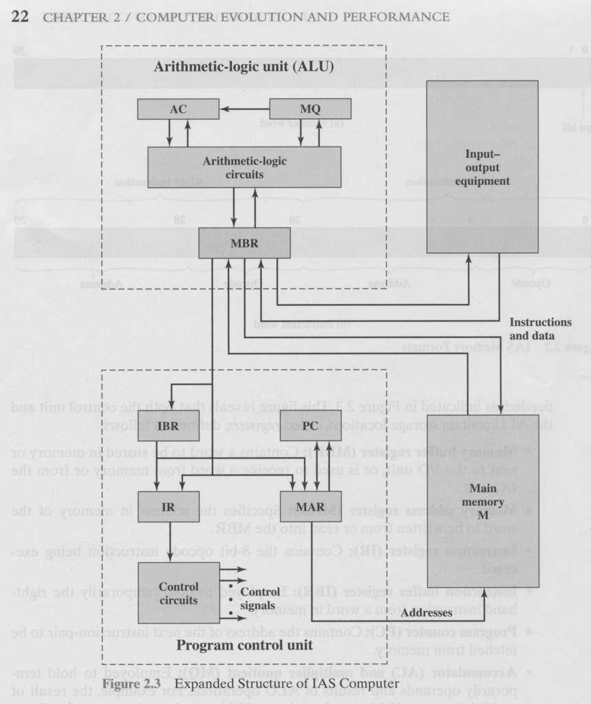
2 The IAS machine language instructions are 20 bits long and have the following form:op-code memory-address, where op-code is an 8-bit operation code and memory-address is a 12-bit memory address. The table above lists the complete IAS instruction set. There are 22 machine instructions for the IAS computer, each associated with an 8-bit op-code, as shown in the table below. Note that the opcode is given in decimal but, of course, is stored in the computer in binary. Note also that not all instructions require a memory address, in which case the last 12 bits of the instruction are ignored. For example, the machine language statement says to get the data in Selectron memory location 14 and load it into the AC. Since each addressable cell in memory (each word) contains 40 bits, two instructions fit in each word of memory. If the word is used to store data instead of instructions, then all 40 bits are used to store one data value. Data Path Below is the diagram of the CPU data paths for the IAS computer. This comes from Stallings 2010; the register labeled MQ is the register we have been calling AR (arithmetic register). 2
3 3


4 1.2.2 INSTRUCTION INTERPRETATION CYCLE Interpretation of an instruction proceeds in three steps or cycles. The instruction is fetched, decoded, and executed. These three steps are discussed in the following sub sections. Instruction Fetch A partial flow chart for the instruction fetch cycle is shown in Figure 1.6. Because two instructions are fetched at once, the first step is to determine if a fetch from memory is required. This test is made by testing the least-significant bit (LSB) of the program counter. Thus, an instruction fetch from memory occurs only on every other state of the PC or if the previous instruction is a taken branch. The fetch from memory places a left (L) and a right (R) instruction in the instruction buffer register (IBR). Instructions are executed, except for the case of a branch instruction, left, right, left, right, etc. For example, consider that an R instruction has just been completed. Figure 1.6 Instruction fetch cycle 4
5 There is no instruction in the IBR and a reference is made to memory to fetch an instruction pair. Normally, the L instruction is then executed. The path follows to the left, placing the instruction into the instruction register (IR). The R instruction remains in the IBR for use on the next cycle, thereby saving a memory cycle to fetch the next instruction. If the prior instruction had been a branch to the R instruction of the instruction pair, the L instruction is not required, and the R instruction is moved to the IR. In summary, the instruction sequence is as follows: Sequence L followed by R R followed by L L branch to L R branch to R L branch to R R branch to L Action No memory access required Increment PC, access memory, use L instruction Memory access required and L instruction used Memory access required and R instruction used If in same computer word, memory access not required If in same computer word, memory access not required After the instruction is decoded and executed, the PC is incremented for the next instruction and control returns to the start point. Decode and Execute Instruction decode is only indicated in Figure 1.6. However, the instruction has been placed in the IR. As shown in Figure 1.7, combinatorial logic in the control unit decodes the op-code and decides which of the instructions will be executed. In other words, decoding is similar to the CASE statement of many programming languages. The flow charts for two instruction executions are shown in Figure 1.7: numbers 21 and 6. After an instruction is executed, control returns to the instruction fetch cycle, shown in Figure

6 Figure 1.7 Decode and execute The sequencing of the instruction interpretation cycle is controlled by a hardwired state machine, discussed in Chapter 5. Each of the states is identified in flowchart form, flip flops are assigned to represent each state, and the logic is designed to sequence through the states. After the invention of microprogramming, the flow chart is reduced to a series of instructions that are executed on the micromachine. In other words, a second computer, rather than a hardwired state machine, provides the control. Addressing Modes & CPU Internals In the following descriptions I will use a hypothetical 3-operand ADD instruction: ADD Dest, Src1, Src2 and use different addressing modes for Src2. 6
7 Note that I am ignoring the Src1 and Dest operands. These, too, could use any of the following addressing modes. Immediate Addressing ADD Dest, Src1, literal value The operand's value is encoded in the instruction as a literal value. It may be treated as signed or unsigned depending on the instruction. MIPS example: addi $t1, $t2, 100 Literal values are known on some architectures as immediate values. Register Mode ADD Dest, Src, Register A register number is specified in the instruction; the operand's value comes from the register. MIPS example: add $t1, $t2, $t3 Absolute or Direct Mode ADD Dest, Src, memory address The instruction encodes a memory address; the operand's value is loaded from that address. Note that most RISC ISAs only provide memory addressing for load & store instructions. CISC ISAs usually allow memory addressing for many instructions. MIPS example: lw $t1, 5000 Register Indirect Mode ADD Dest, Src, (Register) The instruction encodes a register number. The value in the register is treated as an address; the operand's value is loaded from that address. The register is effectively a pointer: instead of holding a value, the register points at the location in memory where that value exists. 7
8 MIPS example: lw $t1, ($t2) The idea of a pointer is used in many languages to create dynamic data structures, e.g. linked lists. In Java, a linked list of ints can be created with: public class IntList { private int x; private IntList next; } although the next variable is strictly a reference, not a pointer: Java stops you from seeing the address. In C, we can do: struct IntList { int x; struct IntList *next; } and the next variable is a pointer which holds an address and which is directly visible to the programmer. Indexed Absolute Mode ADD Dest, Src, base(register) The instruction encodes a literal value, the base, and a register number. The literal value, with the register's value added, is treated as an address; the operand's value is loaded from that address. The register is known as an index register. MIPS example: lw $t1, 300($t2) This allows the low-level implementation of arrays. Assume that an array of 25 characters, name[], is stored starting at memory address 50 onwards. The character name[0] is stored at location 50, name[1] at 51, name[2] at 52 etc. A program can loop with register Rn going from 0 up to 24. The operand 50(Rn) would access each of the characters in the array from position 0 up to 24. 8
9 Note that, for arrays of different type sizes, e.g. 32-bit ints, the index register has to be incremented by the byte size of the elements (i.e. 4) each time through the loop. This addressing mode is useful when the array is fixed in memory: for example, it is a global array defined at compile time. The rest of the addressing modes below are seen mainly on CISC architectures. Base plus Offset Mode ADD Dest, Src, BaseRegister(offset) This time, the offset is the fixed literal, and the base of the data structure is obtained from a register. This addressing mode is useful to access specific fields of a structure or object. Consider a structure of different-sized fields, e.g. a C struct: struct Student { int id; # 32-bit value short age; # 16-bit value char gender; # 8-bit value } The id field is at offset 0 in the struct, the age field is at offset 4, and the gender field is at offset 6. Imagine you have a Student struct variable s1, and you want to set the age in the struct to 23: s1.age = 23; If register R5 (playing the role of s1) points at the base of the struct, then the following would do the work: StoreHalfword R5(4), 23 as we know the age field is 4 bytes from the address that R5 points to. Base plus Index Mode ADD Dest, Src, BaseRegister(IndexRegister) Instead of encoding the base as a fixed literal value, the base value comes from a register. The values of the two registers are added together to form the address of the value to access. 9
10 The base register is effectively a pointer to some data structure like an array, and the index pointer is the index into that array. This is useful when the data structure's location is not defined at compiletime, but is created at run-time by the program: o the structure might be a local variable, created when the function starts. o the structure might be dynamically allocated, e.g. with C's malloc() or Java's new operator. Assuming that the base register points at the base of the structure, this addressing mode can access the fields or elements in the structure. Base plus Index plus Offset Mode ADD Dest, Src, BaseRegister(IndexRegister)offset The instruction encodes two registers and a literal value which is the offset The values of all three are added together to form the address of the value to access. This addressing mode is useful when there is an array of structs/objects, and you want to access a specific field within one of the objects, e.g. studentlist[57].age = 23; The base register would point at the base of the array, the index would hold 57 * sizeof(student), and the offset would be the offset of the age field from the base of each struct/object. Register Pre-increment/Pre-decrement Mode ADD Dest, Src, +Register or -Register The value in the register is pre-incremented or pre-decremented before it is used. This mode often appears in combination with the other addressing modes above. Used in many 1960s and 1970s ISAs, its use on the PDP-11 CPU inspired the pre-increment & pre-decrement operators in C, which have been adopted by its decendants like Java, i.e. ++x; 10
11 Register Post-increment/Post-decrement Mode ADD Dest, Src, Register+ or Register- The value in the register is incremented or decremented after it is used. This mode often appears in combination with the other addressing modes above. Memory Indirect Mode ADD Dest, Src, (memory address) The value at the given memory address is fetched, and this is used as a pointer to the actual memory location. If you ever get to write a substantial amount of C programming, you will see this in action as a pointer to a pointer. As shown above, there is a single indirection: fetch the value to get the address, fetch the value at that address. On some systems, e.g. the PDP-10 minicomputer, the word size (i.e. data bus size) was much bigger than the address bus size, so there were extra bits left over in each word which were not needed as an address. One specific bit in a word was treated as an indirect bit: o if it was set, then the CPU would treat the value as another address, and go and fetch the value at this address. This implies that you could chain addresses: one address could point at another one, which could point at a further one etc. One prank was to set the indirect bit in a word in memory, and put the address of that word in the word itself. o Accesses to this location would cause the CPU to go into an endless loop of indirections. o On some implementations of the PDP-10 ISA, this would lock the CPU up hard, and it would need to be powered down to fix the problem. Data Transfer & Manipulation Computer provides an extensive set of instructions to give the user the flexibility to carryout various computational task. Most computer instruction can be classified into three categories. 11
12 (1) Data transfer instruction (2) Data manipulation instruction (3) Program control instruction Data transfer instruction cause transferred data from one location to another without changing the binary instruction content. Data manipulation instructions are those that perform arithmetic logic, and shift operations. Program control instructions provide decision-making capabilities and change the path taken by the program when executed in the computer. (1) Data Transfer Instruction Data transfer instruction move data from one place in the computer to another without changing the data content. The most common transfers are between memory and processes registers, between processes register & input or output, and between processes register themselves (Typical data transfer instruction) Name Load Store Move Exchange Input Output Push Pop Mnemonic LD ST MOV XCH IN OUT PUSH POP (2) Data Manipulation Instruction It performs operations on data and provides the computational capabilities for the computer. The data manipulation instructions in a typical computer are usually divided into three basic types. (a) Arithmetic Instruction (b) Logical bit manipulation Instruction (c) Shift Instruction. 12
13 (a) Arithmetic Instruction Name Increment Decrement Add Subtract Multiply Divide Add with Carry Subtract with Basses Negate (2 s Complement) Mnemonic INC DEC Add Sub MUL DIV ADDC SUBB NEG (b) Logical & Bit Manipulation Instruction Name Clear Complement AND OR Exclusive-Or Clear Carry Set Carry Complement Carry Enable Interrupt Disable Interrupt Mnemonic CLR COM AND OR XOR CLRC SETC COMC ET OI (c) Shift Instruction Instructions to shift the content of an operand are quite useful and one often provided in several variations. Shifts are operation in which the bits of a word are moved to the left or right. The bit-shifted in at the and of the word determines the type of shift used. Shift instruction may specify either logical shift, arithmetic shifts, or rotate type shifts. Name Logical Shift right Logical Shift left Arithmetic shift right Arithmetic shift left Rotate right Rotate left 13 Mnemonic SHR SHL SHRA SHLA ROR ROL
14 Rotate mgmt through carry Rotate left through carry RORC ROLC Computer Bus Structure A bus is a collection of wires that connect several devices within a computer system. When a word of data is transferred between units, all its bits are transferred in parallel. A computer must have some lines for addressing and control purposes. Three main groupings of lines: 1. Data Bus. This is for the transmission of data. 2. Address Bus. This specifies the location of data in MM. Control Bus. This indicates the direction of data transfer and coordinates the timing of events during the transfer. Single Bus Structure All units are connected to a single bus, so it provides the sole means of interconnection. Single bus structure has advantages of simplicity and low cost. Single bus structure has disadvantages of limited speed since usually only two units can participate in a data transfer at any one time. This means that an arbitration system is required and that units will be forced to wait. Only two units can actively use the bus at any given time. Bus control lines are used to arbitrate multiple requests for the use of the bus. Buffer Registers are used to hold information during transfers. 14
15 Two Bus Structure In the first configuration, the processor is placed between the I/O unit and the memory unit. The processor is responsible for any data transfer between the I/O unit and the memory unit. The processor acts as a messenger. In this structure, the processor performance and capability is not being maximized. Most of the time, the processor is doing data transfer between these units instead of performing more complex applications. Also, the processor is idle most of the time waiting for these slow devices. In the second configuration, I/O transfers are made directly to or from the memory. A special purpose processor called peripheral processor or I/O channel is needed as part of the I/O equipment to control and facilitate such transfers. This special processor is the direct memory access(dma) controller. It allows main memory to perform data transfer between I/O units. 15
16 MICRO-PROGRAMMED VERSUS HARDWIRED CONTROL UNITS: The Basic Computer Every student of computer science knows that all traditional digital computers have two principal functional parts: the data path section in which processing occurs and the control section which is responsible for decoding instructions and leaving the correct sequence of control signals to make the processing happen in the data path.. Basically there are two types of control units: hard-wired controllers and microprogrammed controllers. In order to appreciate the difference and see how computers really work, we present a very simple computer. A block diagram of its data path sections is shown in Figure 1. A single 12-bit-wide bus provides for exchange of information between pairs of registers within the data path section. The registers and the 256 X 12 bit RAM memory are controlled by 16 control signals. Most of the registers have Load (L) and Enabled (E) signals. An active L signal to a register causes the contents of the bus to be clocked into that register on the next rising pulse from the system clock. An active E signal enables the tristate outputs of the register, thereby making its contents available to the bus. Therefore, a register transfer from, for example, register A to register B would require active EA and LB control signals. Processing of data is done by the Arithmetic-Logic-Unit (ALU), a circuit that is capable of adding or subtracting the 12-bit numbers contained in its two input registers: the accumulator (ACC) and register B. The operation performed by the ALU is selected by the Add (A) or Subtract (S) control signals. The accumulator also contains a single flip-flop that is set whenever its contents are negative (i.e., whenever the leading bit is set--meaning a negative 2's complement number). The value of this "negative flag" provides input to the controller/sequencer, and, as we shall see, permits implementation of conditional branching instructions. The machine's RAM memory is accessed by first placing the 8-bit address in the Memory Address Register (MAR). An active Read (R) control signal to the RAM will then cause the selected word from the RAM to appear in the Memory Data Register (MDR). An active Write (W) signal, on the other hand, will cause the word contained in the MDR to be stored in the RAM at the address specified by the MAR. Since there are no input or output ports in this simple computer, all I/O is memory mapped. In other words, several memory locations are reserved for input/output devices. Memory reads from any of those locations will cause data from the corresponding input device to appear in the MDR; memory writes to them will cause data in the MDR to be sent to the corresponding output device. A word stored in any given memory location may 16
17 be data to be manipulated by the computer or a coded instruction that specifies an action to be taken. The data path section also contains a Program Counter (PC) whose function it is to point to the address in RAM of the next instruction to be executed. The Increment Program Counter (IP) control signal causes the contents of the PC to increase by one. Since, as we shall see, instructions on this machine are one word long, this provides a simple mechanism for sequential instruction execution. In addition there is an Instruction Register (IR) which holds the instruction that is about to be execute and provides its opcode to the controller/sequencer. The Computer's Instruction Set An instruction on our simple computer consists of one 12-bit word. The leading four bits form the operation code (opcode) which specifies the action to be taken, and the remaining 8 bits, when used, indicate the memory address of one of the instruction's operands. For those instructions that have two operands, the other operand is always contained within the accumulator. Table 1 gives eight instructions that form the instruction set we have chosen for our machine. Also shown in the table is the sequence of control signals necessary for execution of each of the instructions in the machine's instruction set and for fetching the next instruction. In each case the register transfers required for execution of each step are shown. For example, in the case of the LDA (load accumulator) instruction, the first step consists of copying the address of the operand, contained in the least significant 8 bits of the instruction register, to the memory address register. Thus the EI (enable IR) and LM (load MAR) control signals are active. The next step is to read the operand from memory into the memory data register. An active R (memory read) signal performs that task. The last step required to execute the LDA instruction is to copy the contents of the memory data register to the accumulator. Active ED (enable MDR) and LA (load accumulator) do the trick. The Hard-Wired Control Unit Figure 2 is a block diagram showing the internal organization of a hard-wired control unit for our simple computer. Input to the controller consists of the 4-bit opcode of the instruction currently contained in the Instruction Register and the negative flag from the accumulator. The controller's output is a set of 16 control signals that go out to the various registers and to the memory of the computer, in addition to a HLT signal that is activated whenever the leading bit of the op-code is one. The controller is 17
18 composed of the following functional units: A ring counter, an instruction decoder, and a control matrix. The ring counter provides a sequence of six consecutive active signals that cycle continuously. Synchronized by the system clock, the ring counter first activates its T0 line, then its T1 line, and so forth. After T5 is active, the sequence begins again with T0. Figure 3 shows how the ring counter might be organized internally. The instruction decoder takes its four-bit input from the op-code field of the instruction register and activates one and only one of its 8 output lines. Each line corresponds to one of the instructions in the computer's instruction set. Figure 4 shows the internal organization of this decoder. The most important part of the hard-wired controller is the control matrix. It receives input from the ring counter and the instruction decoder and provides the proper sequence of control signals. Figure 5 is a diagram of how the control matrix for our simple machine might be wired. To understand how this diagram was obtained, we must look carefully at the machine's instruction set (Table 1). Table 2 shows which control signals must be active at each ring counter pulse for each of the instructions in the computer's instruction set (and for the instruction fetch operation). The table was prepared by simply writing down the instructions in the left-hand column. (In the circuit these will be the output lines from the decoder). The various control signals are placed horizontally along the top of the table. Entries into the table consist of the moments (ring counter pulses T0, T1, T2, T3, T4, or T5) at which each control signal must be active in order to have the instruction executed. This table is prepared very easily by reading off the information for each instruction given in Table 1. For example, the Fetch operation has the EP and LM control signals active at ring count 1, and ED, LI, and IPC active at ring count 2. Therefore the first row (Fetch) of Table 2 has T0 entered below EP and LM, T1 below R, and T2 below IP, ED, and LI. Once Table 2 has been prepared, the logic required for each control signal is easily obtained. For each an AND operation is performed between any active ring counter (Ti) signals that were entered into the signal's column and the corresponding instruction contained in the far left-hand column. If a column has more than one entry, the output of the ANDs are ORed together to produce the final control signal. For example, the LM column has the following entries: T0 (Fetch), T3 associated with the LDA instruction, and T3 associated with the STA instruction. Therefore, the logic for this signal is: LM = T0 + T3*LDA + T3*STA 18
19 This means that control signal LM will be activated whenever any of the following conditions is satisfied: (1) ring pulse T0 (first step of an instruction fetch) is active, or (2) an LDA instruction is in the IR and the ring counter is issuing pulse 3, or (3) and STA instruction is in the IR and the ring counter is issuing pulse 3. The entries in the JN (Jump Negative) row of this table require some further explanation. The LP and EI signals are active during T3 for this instruction if and only if the accumulator's negative flag has been set. Therefore the entries that appear above these signals for the JN instruction are T3*NF, meaning that the state of the negative flag must be ANDed in for the LP and EI control signals. Figure 6 gives the logical equations required for each of the control signals used on our machine. These equations have been read from Table 2, as explained above. The circuit diagram of the control matrix (Figure 5) is constructed directly from these equations. It should be noticed that the HLT line from the instruction decoder does not enter the control matrix, Instead this signal goes directly to circuitry (not shown) that will stop the clock and thus terminate execution. A Micro-programmed Control Unit As we have seen, the controller causes instructions to be executed by issuing a specific set of control signals at each beat of the system clock. Each set of control signals issued causes one basic operation (micro-operation), such as a register transfer, to occur within the data path section of the computer. In the case of a hardwired control unit the control matrix is responsible for sending out the required sequence of signals. An alternative way of generating the control signals is that of micro-programmed control. In order to understand this method it is convenient to think of sets of control signals that cause specific micro-operations to occur as being "microinstructions" that could be stored in a memory. Each bit of a microinstruction might correspond to one control signal. If the bit is set it means that the control signal will be active; if cleared the signal will be inactive. Sequences of microinstructions could be stored in an internal "control" memory. Execution of a machine language instruction could then be caused by fetching the proper sequence of microinstructions from the control memory and sending them out to the data path section of the computer. A sequence of microinstructions that implements an instruction on the external computer is known as a micro-routine. The instruction set of the computer is thus determined by the set of micro-routines, the"microprogram," stored in the controller's memory. The control 19
20 unit of a microprogram-controlled computer is essentially a computer within a computer. Figure 7 is a block diagram of a micro-programmed control unit that may be used to implement the instruction set of the computer we described above. The heart of the controller is the control 32 X 24 ROM memory in which upt to bit long microinstructions can be stored. Each is composed of two main fields: a 16-bit wide control signal field and an 8-bit wide next-address field. Each bit in the control signal field corresponds to one of the control signals discussed above. The next-address field contains bits that determine the address of the next microinstruction to be fetched from the control ROM. We shall see the details of how these bits work shortly. Words selected from the control ROM feed the microinstruction register. This 24-bit wide register is analogous to the outer machine's instruction register. Specifically, the leading 16 bits (the control-signal field) of the microinstruction register are connected to the control-signal lines that go to the various components of the external machine's data path section. Addresses provided to the control ROM come from a micro-counter register, which is analogous to the external machine's program counter. The micro-counter, in turn, receives its input from a multiplexer which selects from : (1) the output of an address ROM, (2) a current-address incrementer, or (3) the address stored in the next-address field of the current microinstruction. The logic that selects one of these three alternatives will be explained shortly. The controller's address ROM is fed by the outer computer's instruction register. The address ROM maps the op-code of the instruction currently contained in the op-code field of the instruction register to the starting address of the corresponding microroutine in the control ROM. Address zero of the address ROM contains the control-rom address of the fetch routine; each other addresses in the address-rom corresponds to one of the op-codes of the computer's instruction set. Table 3 shows the contents of the address ROM for the instruction set of our simple computer. To see how the address ROM works, let us assume that an ADD instruction has been fetched into the outer computer's instruction register. Since the op-code of the ADD instruction is 3, the number stored at location 3 of the address ROM (a 9) is the starting address in the control ROM of the microroutine that implements the ADD instruction. Details of a microinstruction's next address field are shown in Figure 8. The 5-bit CRJA (Control ROM Jump Address) sub-field holds a microinstruction address. Thus, the address of the next microinstruction may be obtained from the current microinstruction. This permits branching to other sections within the microprogram. 20
21 The combination of the MAP bit, the CD (condition) bit, and the negative flag from the accumulator of the external machine provide input to the logic that feeds the select lines of the multiplexer and thereby determine how the address of the next microinstruction will be obtained. If the MAP bit is one, the logic attached to the multiplexer's select lines produces a 01 which selects the address ROM. Therefore, the address of the micro-routine corresponding to the instruction in the outer machine's instruction register will be channeled to the control ROM. It should be clear that the MAP bit must be set in the last microinstruction of the "fetch" micro-routine, since it is at that moment that we want the newly-fetched instruction to be executed. If the MAP bit is zero and the CD bit is zero, (unconditional branch), the multiplexer logic produces a 10, which selects the CRJA field of the current instruction. Therefore, the next instruction will come from the address contained in the current instruction's next-address field. With MAP=0 and CD=1 (conditional branch), the logic that feeds the multiplexer will produce either a 00 or a 10, depending on the value of the negative flag. If the flag is set, it is a 10, which selects the jump address contained in the current microinstruction. If the negative flag is cleared, the select lines to the multiplexer receive a 00, which causes the incrementer to be selected. The next microinstruction will come from the next address in sequence. It should be noticed that with this scheme, if we are not doing branching, the CRJA field should contain the address of the next microinstruction and the CD bit should be cleared. This will cause "branch to the next microinstruction" to occur. The one exception to this rule is the case of the last microinstruction within a micro-routine. Normally we would then want to branch back to the "fetch" micro-routine. Since this routine starts at control-rom location 00000, that address should be contained in the CRJA field and CD should be 0. The HLT bit is used to terminate execution. If it is set, the clock that synchronizes activities within the entire machine is stopped. Notice that the micro-counter is triggered by a rising clock edge, and the microinstruction register by a falling edge. Thus, we see that on each positive edge, the micro-counter receives the address of the microinstruction and presents it to the control ROM, which has until the next negative edge to output the addressed control word to the microinstruction register. Since all operation in the data path section are positive-edge triggered, there is adequate time for the signals specified in the control word contained in the microinstruction register to go out to all sections of the external machine. The sequence of latching the address of microinstruction i+1 into the microcounter while microinstruction i executes (positive edge) and then presenting the 21
22 control word of microinstruction i+1 to the microinstruction register (negative edge) continues until a set HLT bit stops the clock. Table 4 shows a microprogram which, when loaded into the control ROM, will implement the instruction set of the computer we have been describing. For each microinstruction, the control ROM address has been expressed in hexadecimal, and the contents in binary. The order of the bits in the control signal field is the same as that shown in table 2: IP, LP, EP, LM, R, W, LD, ED, LI, EI, LA, EA, A, S, EU, LB, reading from left to right. The last four columns of table 4 express the status of the CD, MAP, and HLT bits, and the Control ROM Jump Address, expressed in hexadecimal. In order to clarify how the microprogram works, a description is now given of the "fetch" and JN (jump on negative) micro-routines. The "fetch" micro-routine occupies control ROM addresses 0, 1, and 2. The active EP and LM control-signal bits in its first microinstruction cause a register transfer from the program counter to the memory address register to occur. The MAR will now contain the address in RAM of the next instruction. Since CD and MAP are both zero (unconditional branch), the next microinstruction will come from the address stored in the CRJA field (01) -- the next consecutive location. The microinstruction stored at that location has only the R bit active. Thus, the word stored in the memory location being accessed by the MAR (presumably the next instruction ) will be gated to the Memory Data Register (MDR). The zeroes in CD and MAP again cause the microinstruction to be fetched from the address specified in the CRJA field, (02). Active control signal bits for that microinstruction are ED, LI, and IP. The first two transfer the word in the MDR to the Instruction Register, and the last increments the program counter. The new instruction is safely in the IR, and the PC is pointing to the next instruction in sequence. We have completed an instruction fetch. Since the MAP field in the last microinstruction of this "fetch" micro-routine is equal to 1, the address of the next microinstruction is determined by the address ROM, which, in turn, depends upon the opcode of the instruction that has just been loaded into the instruction register. When the JN instruction is executed, control is supposed to be transferred to the address specified by the least significant eight bits of the number contained in the instruction register if the negative flag is set. If the negative flag is not set, execution should continue with the next instruction in sequence. Let us see how the microroutine stored at control-rom locations 0F, 10, and 11 implement this conditional jump. In the first microinstruction, none of the control signal bits is set. Thus, nothing will occur in the data path section of the computer. However, the fact that the CD bit is set means that IF THE NEGATIVE FLAG IS SET, the next microinstruction will be fetched from the control-rom address specified in the CRJA field (11 in this 22
23 case). The microinstruction stored at that location has the EI and LP control signal bits set. Thus, the contents of the instruction register (the least significant eight bits) will be transferred to the program counter. The zeroes stored in the CD and MAP bits cause the next microinstruction to be fetched from the address contained in the CRJA field -- a 00 in this case. This is the start of the "fetch"micro-routine. Thus we see that if the negative flag is set, the JN micro-routine places the jump address in the program counter and transfer to the fetch routine. When that fetch is performed, control will have been transferred to the jump address. If, on the other hand, the negative flag is NOT SET when the JN micro-routine executes, then the set CD bit in its first microinstruction causes the current address stored in the micro-counter to be incremented. Thus, the next microinstruction would be fetched from location 10. That microinstruction also has no active control signals bits, but with CD=0 and CRJA=00, the next microinstruction will be the first one in the "fetch" routine. Notice that in this case, the JN instruction simply returns us to the next fetch. Since the program counter has not been altered, that fetch will be from the next sequential memory location, as usual. Hardwired vs. Micro-programmed Computers It should be mentioned that most computers today are micro-programmed. The reason is basically one of flexibility. Once the control unit of a hard-wired computer is designed and built, it is virtually impossible to alter its architecture and instruction set. In the case of a micro-programmed computer, however, we can change the computer's instruction set simply by altering the microprogram stored in its control memory. In fact, taking our basic computer as an example, we notice that its four-bit op-code permits up to 16 instructions. Therefore, we could add seven more instructions to the instruction set by simply expanding its microprogram. To do this with the hard-wired version of our computer would require a complete redesign of the controller circuit hardware. Another advantage to using micro-programmed control is the fact that the task of designing the computer in the first place is simplified. The process of specifying the architecture and instruction set is now one of software (micro-programming) as opposed to hardware design. Nevertheless, for certain applications hard-wired computers are still used. If speed is a consideration, hard-wiring may be required since it is faster to have the hardware issue the required control signals than to have a "program" do it. 23
24 FIGURES: Figure 1. A Simple Single-Bus Basic Computer. 24
25 Figure 2. A Block diagram of the Basic Computer's Hard-wired Control unit Figure 3. The Internal Organization of the Ring Counter 25

26 Figure 4. The Internal Organization of the Hard-wired Instruction Decoder 26
27 Figure 5. The Internal Organization of the Hard-wired Control Matrix 27
28 IP = T2 W = T5*STA LP = T3*JMP + T3*NF*JN LD = T4*STA LA = T5*LDA + T4*ADD + T4*SUB EA = T4*STA + T3*MBA EP = T0 S = T3*SUB A = T3*ADD LI = T2 LM = T0 + T3*LDA + T3*STA ED = T2 + T5*LDA R = T1 + T4*LDA EU = T3*ADD+T3*SUB EI = T3*LDA + T3*STA + T3*JMP + T3*NF*JN LB = T3*MBA Figure 6. The logical equations required for each of the hardwired control signals on the basic computer. The machine's control matrix is designed from these equations. 28
29 Figure 7. A Microprogrammed Control Unit for the Simple Computer 29
30 TABLES: Table 1. An Instruction Set For The Basic Computer Instruction Op- Code Execution Register Ring Active Control Mnemonic Action Transfers Pulse Sig nals LDA 1 ACC<--(RAM) 1. MAR <-- IR 3 EI, LM (Load ACC) 2. MDR <-- RAM(MAR) 4 R 3. ACC <-- MDR 5 ED, LA STA 2 (RAM) <--ACC 1. MAR <-- IR 3 EI, LM (Store ACC) 2. MDR <-- ACC 4 EA, LD 3. RAM(MAR) <-- MDR 5 W ADD 3 ACC <-- ACC + B 1. ALU <-- ACC + B 3 A (Add B to ACC) 2. ACC <-- ALU 4 EU, LA SUB 4 ACC <-- ACC - B 1. ALU <-- ACC - B 3 S (Sub. B from ACC) 2. ACC <-- ALU 4 EU, LA MBA 5 B <-- ACC 1. B <-- A 3 EA, LB (Move ACC to B) JMP 6 PC <-- RAM 1. PC <-- IR 3 EI, LP (Jump to Address) 30
31 JN 7 PC <-- RAM 1. PC <-- IR 3 NF: EI, LP (Jump if if negative if NF set Negative) flag is set HLT 8-15 Stop clock "Fetch" IR <-- Next 1. MAR <-- PC 0 EP, LM LI, IP Instruction 2. MDR <-- RAM(MAR) 1 R 3. IR <-- MDR 2 ED, Table 2. A Matrix of Times at which Each Control Signal Must Be Active in Order to Execute the Hard-wired Basic Computer's Instructions Control Signal: IP LP EP LM R W LD ED LI EI LA EA A S EU LB Instruction: "Fetch" T2 T0 T0 T1 T2 T2 LDA T3 T4 T5 T3 T5 STA T3 T5 T4 T3 T4 MBA T3 T3 ADD T4 T3 T4 SUB T4 T3 T4 JMP T3 T3 JN T3*NF T3*NF Table 3. The Microprogrammed Basic Computer's Address ROM Instruction Address-ROM Address Mnemonic Address-ROM Contents (Instruction Op-Code) (Control-ROM Micro- Routine Start Address) "Fetch" 0 00 LDA 1 03 STA 2 06 ADD 3 09 SUB 4 0B 31
32 MBA 5 0D JMP 6 0E JN 7 0F Available for 8-E 12-1E New Instructions HLT F 1F Table 4. The Microprogram that Implements the Basic Computer's Instruction Set Microroutine Address-ROM Micro- Control Signals: CD MAP HLT Address of Comment Name Address Instruction ILELRWLELELEASEL bit bit bit Next Micro- (Mnemonic) (Opcode) Address PPPM DDIIAA UB Instruction "Fetch" Next CR Address = Next CR Address = xx Get CR Address from Address ROM LDA Nexr CR Address = Next CR Address = Next CR Address = 00 (Fetch) STA Next CR Address = Next CR Address = Next CR Address = 00 (Fetch) ADD A Next CR Address = 0A 0A Next CR Address = 00 (Fetch) 32
33 SUB 4 0B C Next CR Address = 0C 0C Next CR Address = 00 (Fetch) MBA 5 0D Next CR Address is 00 (Fetch) JMP 6 0E Change PC; next CR Address is 00 (Fetch) JN 7 0F NF=0: INC CRJA; NF=1: Next CR Address = Next CR Address = 00 (Fetch) Change PC; next CR Address is 00 (Fetch) Available for 8-E 12-1E microinstructions can be added here New HLT F 1F xx Stop Clock 33
TYPES OF INTERRUPTS: -
 There are 3 types of interrupts. TYPES OF INTERRUPTS: - External Interrupts. Internal Interrupts. Software interrupts. Hardware Interrupts (1) External interrupts come from I/O devices, from a timing device
Fig: Computer memory with Program, data, and Stack. Blog - NEC (Autonomous) 1
 1") Central Processing Unit 1. Stack Organization A useful feature that is included in the CPU of most computers is a stack or last in, first out (LIFO) list. A stack is a storage device that stores information
Central Processing Unit 1. Stack Organization A useful feature that is included in the CPU of most computers is a stack or last in, first out (LIFO) list. A stack is a storage device that stores information
10-1 C D Pearson Education, Inc. M. Morris Mano & Charles R. Kime LOGIC AND COMPUTER DESIGN FUNDAMENTALS, 4e
 10-1 C D E A B 10-2 A B A B C (A B) C D A A B (A B) C E D (A B) C D E (A B) C + D E (A B) C 10-3 Opcode Mode Address or operand 10-4 Memory 250 Opcode Mode PC = 250 251 ADRS 252 Next instruction ACC Opcode:
TABLE 9-1. Symbolic Convention for Addressing Modes. Register indirect LDA (R1) ACC M[ R1] Refers to Figure 9-4. Addressing mode. Symbolic convention
![TABLE 9-1. Symbolic Convention for Addressing Modes. Register indirect LDA (R1) ACC M[ R1] Refers to Figure 9-4. Addressing mode. Symbolic convention](/thumbs/78/77835871.jpg "TABLE 9-1. Symbolic Convention for Addressing Modes. Register indirect LDA (R1) ACC M[ R1] Refers to Figure 9-4. Addressing mode. Symbolic convention") T-236 Symbolic Convention for Addressing Modes TABLE 9-1 Symbolic Convention for Addressing Modes Refers to Figure 9-4 Addressing mode Symbolic convention Register transfer Effective address Contents of
T-236 Symbolic Convention for Addressing Modes TABLE 9-1 Symbolic Convention for Addressing Modes Refers to Figure 9-4 Addressing mode Symbolic convention Register transfer Effective address Contents of
Digital System Design Using Verilog. - Processing Unit Design
 Digital System Design Using Verilog - Processing Unit Design 1.1 CPU BASICS A typical CPU has three major components: (1) Register set, (2) Arithmetic logic unit (ALU), and (3) Control unit (CU) The register
Chapter 4. MARIE: An Introduction to a Simple Computer
 Chapter 4 MARIE: An Introduction to a Simple Computer Chapter 4 Objectives Learn the components common to every modern computer system. Be able to explain how each component contributes to program execution.
Advanced Parallel Architecture Lesson 3. Annalisa Massini /2015
 Advanced Parallel Architecture Lesson 3 Annalisa Massini - 2014/2015 Von Neumann Architecture 2 Summary of the traditional computer architecture: Von Neumann architecture http://williamstallings.com/coa/coa7e.html
Basic Processing Unit: Some Fundamental Concepts, Execution of a. Complete Instruction, Multiple Bus Organization, Hard-wired Control,
 UNIT - 7 Basic Processing Unit: Some Fundamental Concepts, Execution of a Complete Instruction, Multiple Bus Organization, Hard-wired Control, Microprogrammed Control Page 178 UNIT - 7 BASIC PROCESSING
Chapter 3 : Control Unit
 3.1 Control Memory Chapter 3 Control Unit The function of the control unit in a digital computer is to initiate sequences of microoperations. When the control signals are generated by hardware using conventional
Computer Architecture
 Computer Architecture Lecture 1: Digital logic circuits The digital computer is a digital system that performs various computational tasks. Digital computers use the binary number system, which has two
COMPUTER HARDWARE. Instruction Set Architecture
 COMPUTER HARDWARE Instruction Set Architecture Overview Computer architecture Operand addressing Addressing architecture Addressing modes Elementary instructions Data transfer instructions Data manipulation
Introduction to CPU Design
 ١ Introduction to CPU Design Computer Organization & Assembly Language Programming Dr Adnan Gutub aagutub at uqu.edu.sa [Adapted from slides of Dr. Kip Irvine: Assembly Language for Intel-Based Computers]
Module 5 - CPU Design
 Module 5 - CPU Design Lecture 1 - Introduction to CPU The operation or task that must perform by CPU is: Fetch Instruction: The CPU reads an instruction from memory. Interpret Instruction: The instruction
Chapter 17. Microprogrammed Control. Yonsei University
 Chapter 17 Microprogrammed Control Contents Basic Concepts Microinstruction Sequencing Microinstruction Execution TI 8800 Applications of Microprogramming 17-2 Introduction Basic Concepts An alternative
Chapter 4. MARIE: An Introduction to a Simple Computer. Chapter 4 Objectives. 4.1 Introduction. 4.2 CPU Basics
 Chapter 4 Objectives Learn the components common to every modern computer system. Chapter 4 MARIE: An Introduction to a Simple Computer Be able to explain how each component contributes to program execution.
PROBLEMS. 7.1 Why is the Wait-for-Memory-Function-Completed step needed when reading from or writing to the main memory?
 446 CHAPTER 7 BASIC PROCESSING UNIT (Corrisponde al cap. 10 - Struttura del processore) PROBLEMS 7.1 Why is the Wait-for-Memory-Function-Completed step needed when reading from or writing to the main memory?
COMPUTER ARCHITECTURE AND ORGANIZATION Register Transfer and Micro-operations 1. Introduction A digital system is an interconnection of digital
 Register Transfer and Micro-operations 1. Introduction A digital system is an interconnection of digital hardware modules that accomplish a specific information-processing task. Digital systems vary in
csitnepal Unit 3 Basic Computer Organization and Design
 Unit 3 Basic Computer Organization and Design Introduction We introduce here a basic computer whose operation can be specified by the resister transfer statements. Internal organization of the computer
Chapter 5. Computer Architecture Organization and Design. Computer System Architecture Database Lab, SANGJI University
 Chapter 5. Computer Architecture Organization and Design Computer System Architecture Database Lab, SANGJI University Computer Architecture Organization and Design Instruction Codes Computer Registers
THE MICROPROCESSOR Von Neumann s Architecture Model
 THE ICROPROCESSOR Von Neumann s Architecture odel Input/Output unit Provides instructions and data emory unit Stores both instructions and data Arithmetic and logic unit Processes everything Control unit
MARIE: An Introduction to a Simple Computer
 MARIE: An Introduction to a Simple Computer Outline Learn the components common to every modern computer system. Be able to explain how each component contributes to program execution. Understand a simple
CHAPTER 5 Basic Organization and Design Outline Instruction Codes Computer Registers Computer Instructions Timing and Control Instruction Cycle
 CS 224: Computer Organization S.KHABET CHAPTER 5 Basic Organization and Design Outline Instruction Codes Computer Registers Computer Instructions Timing and Control Instruction Cycle Memory Reference Instructions
Class Notes. Dr.C.N.Zhang. Department of Computer Science. University of Regina. Regina, SK, Canada, S4S 0A2
 Class Notes CS400 Part VI Dr.C.N.Zhang Department of Computer Science University of Regina Regina, SK, Canada, S4S 0A2 C. N. Zhang, CS400 83 VI. CENTRAL PROCESSING UNIT 1 Set 1.1 Addressing Modes and Formats
MARIE: An Introduction to a Simple Computer
 MARIE: An Introduction to a Simple Computer 4.2 CPU Basics The computer s CPU fetches, decodes, and executes program instructions. The two principal parts of the CPU are the datapath and the control unit.
CHAPTER SIX BASIC COMPUTER ORGANIZATION AND DESIGN
 CHAPTER SIX BASIC COMPUTER ORGANIZATION AND DESIGN 6.1. Instruction Codes The organization of a digital computer defined by: 1. The set of registers it contains and their function. 2. The set of instructions
Introduction. 3 major parts of CPU : Fig Design Examples of simple CPU. In this chapter : Chap. 8. Chap. 8 Central Processing Unit
 Central Processing Unit 8-1 Introduction 3 major parts of CPU : Fig. 8-1 1) Register Set 2) ALU 3) Control Design Examples of simple CPU Hardwired Control : Chap. 5 Microprogrammed Control : Chap. 7 In
 Part A Questions 1. What is an ISP? ISP stands for Instruction Set Processor. This unit is simply called as processor which executes machine instruction and coordinates the activities of other units..
Advanced Parallel Architecture Lesson 3. Annalisa Massini /2015
 Advanced Parallel Architecture Lesson 3 Annalisa Massini - Von Neumann Architecture 2 Two lessons Summary of the traditional computer architecture Von Neumann architecture http://williamstallings.com/coa/coa7e.html
5-1 Instruction Codes
 Chapter 5: Lo ai Tawalbeh Basic Computer Organization and Design 5-1 Instruction Codes The Internal organization of a digital system is defined by the sequence of microoperations it performs on data stored
Blog - https://anilkumarprathipati.wordpress.com/
 Control Memory 1. Introduction The function of the control unit in a digital computer is to initiate sequences of microoperations. When the control signals are generated by hardware using conventional
COMPUTER ORGANIZATION AND ARCHITECTURE
 Page 1 1. Which register store the address of next instruction to be executed? A) PC B) AC C) SP D) NONE 2. How many bits are required to address the 128 words of memory? A) 7 B) 8 C) 9 D) NONE 3. is the
Materials: 1. Projectable Version of Diagrams 2. MIPS Simulation 3. Code for Lab 5 - part 1 to demonstrate using microprogramming
 CS311 Lecture: CPU Control: Hardwired control and Microprogrammed Control Last revised October 18, 2007 Objectives: 1. To explain the concept of a control word 2. To show how control words can be generated
Architecture & Instruction set of 8085 Microprocessor and 8051 Micro Controller
 of 8085 microprocessor 8085 is pronounced as "eighty-eighty-five" microprocessor. It is an 8-bit microprocessor designed by Intel in 1977 using NMOS technology. It has the following configuration 8-bit
UNIT-II. Part-2: CENTRAL PROCESSING UNIT
 Page1 UNIT-II Part-2: CENTRAL PROCESSING UNIT Stack Organization Instruction Formats Addressing Modes Data Transfer And Manipulation Program Control Reduced Instruction Set Computer (RISC) Introduction:
BASIC COMPUTER ORGANIZATION AND DESIGN
 1 BASIC COMPUTER ORGANIZATION AND DESIGN Instruction Codes Computer Registers Computer Instructions Timing and Control Instruction Cycle Memory Reference Instructions Input-Output and Interrupt Complete
Computer Architecture Programming the Basic Computer
 4. The Execution of the EXCHANGE Instruction The EXCHANGE routine reads the operand from the effective address and places it in DR. The contents of DR and AC are interchanged in the third microinstruction.
MICROPROGRAMMED CONTROL
 MICROPROGRAMMED CONTROL Hardwired Control Unit: When the control signals are generated by hardware using conventional logic design techniques, the control unit is said to be hardwired. Micro programmed
SCRAM Introduction. Philipp Koehn. 19 February 2018
 SCRAM Introduction Philipp Koehn 19 February 2018 This eek 1 Fully work through a computer circuit assembly code Simple but Complete Random Access Machine (SCRAM) every instruction is 8 bit 4 bit for op-code:
Register Transfer and Micro-operations
 Register Transfer Language Register Transfer Bus Memory Transfer Micro-operations Some Application of Logic Micro Operations Register Transfer and Micro-operations Learning Objectives After reading this
2 MARKS Q&A 1 KNREDDY UNIT-I
 2 MARKS Q&A 1 KNREDDY UNIT-I 1. What is bus; list the different types of buses with its function. A group of lines that serves as a connecting path for several devices is called a bus; TYPES: ADDRESS BUS,
Blog -
 . Instruction Codes Every different processor type has its own design (different registers, buses, microoperations, machine instructions, etc) Modern processor is a very complex device It contains Many
Chapter 4. Chapter 4 Objectives. MARIE: An Introduction to a Simple Computer
 Chapter 4 MARIE: An Introduction to a Simple Computer Chapter 4 Objectives Learn the components common to every modern computer system. Be able to explain how each component contributes to program execution.
Lecture 11: Control Unit and Instruction Encoding
 CSCI25 Computer Organization Lecture : Control Unit and Instruction Encoding Ming-Chang YANG mcyang@cse.cuhk.edu.hk Reading: Chap. 7.4~7.5 (5 th Ed.) Recall: Components of a Processor Register file: a
CC312: Computer Organization
 CC312: Computer Organization Dr. Ahmed Abou EL-Farag Dr. Marwa El-Shenawy 1 Chapter 4 MARIE: An Introduction to a Simple Computer Chapter 4 Objectives Learn the components common to every modern computer
Introduction to Computers - Chapter 4
 Introduction to Computers - Chapter 4 Since the invention of the transistor and the first digital computer of the 1940s, computers have been increasing in complexity and performance; however, their overall
8051 Overview and Instruction Set
 8051 Overview and Instruction Set Curtis A. Nelson Engr 355 1 Microprocessors vs. Microcontrollers Microprocessors are single-chip CPUs used in microcomputers Microcontrollers and microprocessors are different
Processing Unit CS206T
 Processing Unit CS206T Microprocessors The density of elements on processor chips continued to rise More and more elements were placed on each chip so that fewer and fewer chips were needed to construct
Lecture1: introduction. Outline: History overview Central processing unite Register set Special purpose address registers Datapath Control unit
 Lecture1: introduction Outline: History overview Central processing unite Register set Special purpose address registers Datapath Control unit 1 1. History overview Computer systems have conventionally
Materials: 1. Projectable Version of Diagrams 2. MIPS Simulation 3. Code for Lab 5 - part 1 to demonstrate using microprogramming
 CPS311 Lecture: CPU Control: Hardwired control and Microprogrammed Control Last revised October 23, 2015 Objectives: 1. To explain the concept of a control word 2. To show how control words can be generated
Basic Computer Organization - Designing your first computer. Acknowledgment: Most of the slides are adapted from Prof. Hyunsoo Yoon s slides.
 Basic Computer Organization - Designing your first computer Acknowledgment: Most of the slides are adapted from Prof. Hyunsoo Yoon s slides. 1 This week- BASIC COMPUTER ORGANIZATION AND DESIGN Instruction
There are four registers involved in the fetch cycle: MAR, MBR, PC, and IR.
 CS 320 Ch. 20 The Control Unit Instructions are broken down into fetch, indirect, execute, and interrupt cycles. Each of these cycles, in turn, can be broken down into microoperations where a microoperation
Computer Organization CS 206 T Lec# 2: Instruction Sets
 Computer Organization CS 206 T Lec# 2: Instruction Sets Topics What is an instruction set Elements of instruction Instruction Format Instruction types Types of operations Types of operand Addressing mode
UNIT:2 BASIC COMPUTER ORGANIZATION AND DESIGN
 1 UNIT:2 BASIC COMPUTER ORGANIZATION AND DESIGN BASIC COMPUTER ORGANIZATION AND DESIGN 2.1 Instruction Codes 2.2 Computer Registers AC or Accumulator, Data Register or DR, the AR or Address Register, program
Computer Organization (Autonomous)
") Computer Organization (Autonomous) UNIT II Sections - A & D Prepared by Anil Kumar Prathipati, Asst. Prof., Dept. of CSE. SYLLABUS Basic Computer Organization and Design: Instruction codes Stored Program
Computer Organization (Autonomous) UNIT II Sections - A & D Prepared by Anil Kumar Prathipati, Asst. Prof., Dept. of CSE. SYLLABUS Basic Computer Organization and Design: Instruction codes Stored Program
Micro-Operations. execution of a sequence of steps, i.e., cycles
 Micro-Operations Instruction execution execution of a sequence of steps, i.e., cycles Fetch, Indirect, Execute & Interrupt cycles Cycle - a sequence of micro-operations Micro-operations data transfer between
Chapter 4 The Von Neumann Model
 Chapter 4 The Von Neumann Model The Stored Program Computer 1943: ENIAC Presper Eckert and John Mauchly -- first general electronic computer. (or was it John V. Atananasoff in 1939?) Hard-wired program
Micro-programmed Control Ch 15
 Micro-programmed Control Ch 15 Micro-instructions Micro-programmed Control Unit Sequencing Execution Characteristics 1 Hardwired Control (4) Complex Fast Difficult to design Difficult to modify Lots of
William Stallings Computer Organization and Architecture 8 th Edition. Chapter 11 Instruction Sets: Addressing Modes and Formats
 William Stallings Computer Organization and Architecture 8 th Edition Chapter 11 Instruction Sets: Addressing Modes and Formats Addressing Modes Immediate Direct Indirect Register Register Indirect Displacement
Machine Instructions vs. Micro-instructions. Micro-programmed Control Ch 15. Machine Instructions vs. Micro-instructions (2) Hardwired Control (4)
 Hardwired Control (4)") Micro-programmed Control Ch 15 Micro-instructions Micro-programmed Control Unit Sequencing Execution Characteristics 1 Machine Instructions vs. Micro-instructions Memory execution unit CPU control memory
Micro-programmed Control Ch 15 Micro-instructions Micro-programmed Control Unit Sequencing Execution Characteristics 1 Machine Instructions vs. Micro-instructions Memory execution unit CPU control memory
Micro-programmed Control Ch 15
 Micro-programmed Control Ch 15 Micro-instructions Micro-programmed Control Unit Sequencing Execution Characteristics 1 Hardwired Control (4) Complex Fast Difficult to design Difficult to modify Lots of
BASIC COMPUTER ORGANIZATION AND DESIGN
 BASIC COMPUTER ORGANIZATION AND DESIGN Instruction Codes Computer Registers Computer Instructions Timing and Control Instruction Cycle Memory Reference Instructions Input-Output and Interrupt Complete
DC57 COMPUTER ORGANIZATION JUNE 2013
 Q2 (a) How do various factors like Hardware design, Instruction set, Compiler related to the performance of a computer? The most important measure of a computer is how quickly it can execute programs.
EE 3170 Microcontroller Applications
 EE 3170 Microcontroller Applications Lecture 4 : Processors, Computers, and Controllers - 1.2 (reading assignment), 1.3-1.5 Based on slides for ECE3170 by Profs. Kieckhafer, Davis, Tan, and Cischke Outline
Computer Organization and Architecture
 Computer Organization and Architecture Dr Binu P Chacko Associate Professor Department of Computer Science Prajyoti Niketan College, Pudukad, THRISSUR Instruction Codes Computer organization is defined
Chapter 1 : Introduction
 Chapter 1 Introduction 1.1 Introduction A Microprocessor is a multipurpose programmable, clock driven, register based electronic device that reads binary instructions from a storage device called memory,
CS311 Lecture: The Architecture of a Simple Computer
 CS311 Lecture: The Architecture of a Simple Computer Objectives: July 30, 2003 1. To introduce the MARIE architecture developed in Null ch. 4 2. To introduce writing programs in assembly language Materials:
Micro-programmed Control Ch 17
 Micro-programmed Control Ch 17 Micro-instructions Micro-programmed Control Unit Sequencing Execution Characteristics Course Summary 1 Hardwired Control (4) Complex Fast Difficult to design Difficult to
STRUCTURE OF DESKTOP COMPUTERS
 Page no: 1 UNIT 1 STRUCTURE OF DESKTOP COMPUTERS The desktop computers are the computers which are usually found on a home or office desk. They consist of processing unit, storage unit, visual display
Hardwired Control (4) Micro-programmed Control Ch 17. Micro-programmed Control (3) Machine Instructions vs. Micro-instructions
 Micro-programmed Control Ch 17. Micro-programmed Control (3) Machine Instructions vs. Micro-instructions") Micro-programmed Control Ch 17 Micro-instructions Micro-programmed Control Unit Sequencing Execution Characteristics Course Summary Hardwired Control (4) Complex Fast Difficult to design Difficult to modify
Micro-programmed Control Ch 17 Micro-instructions Micro-programmed Control Unit Sequencing Execution Characteristics Course Summary Hardwired Control (4) Complex Fast Difficult to design Difficult to modify
ASSEMBLY LANGUAGE MACHINE ORGANIZATION
 ASSEMBLY LANGUAGE MACHINE ORGANIZATION CHAPTER 3 1 Sub-topics The topic will cover: Microprocessor architecture CPU processing methods Pipelining Superscalar RISC Multiprocessing Instruction Cycle Instruction
PESIT Bangalore South Campus
 INTERNAL ASSESSMENT TEST I Date: 30/08/2017 Max Marks: 40 Subject & Code: Computer Organization 15CS34 Semester: III (A & B) Name of the faculty: Mrs.Sharmila Banu.A Time: 8.30 am 10.00 am Answer any FIVE
CS 101, Mock Computer Architecture
 CS 101, Mock Computer Architecture Computer organization and architecture refers to the actual hardware used to construct the computer, and the way that the hardware operates both physically and logically
UNIT-III REGISTER TRANSFER LANGUAGE AND DESIGN OF CONTROL UNIT
 UNIT-III 1 KNREDDY UNIT-III REGISTER TRANSFER LANGUAGE AND DESIGN OF CONTROL UNIT Register Transfer: Register Transfer Language Register Transfer Bus and Memory Transfers Arithmetic Micro operations Logic
Computer Architecture
 http://www.bsccsit.com/ Computer Architecture CSC. 201 Third Semester Prepared By: Arjun Singh Saud Special thanks to Mr. Arjun Singh Saud for providing this valuable note! Chapter 1 Data representation
Unit II Basic Computer Organization
 1. Define the term. Internal Organization-The internal organization of a digital system is defined by the sequence of microoperations it performs on data stored in its registers. Program- A program is
Assembly Language Programming of 8085
 Assembly Language Programming of 8085 Topics 1. Introduction 2. Programming model of 8085 3. Instruction set of 8085 4. Example Programs 5. Addressing modes of 8085 6. Instruction & Data Formats of 8085
BASIC COMPUTER ORGANIZATION AND DESIGN
 1 BASIC COMPUTER ORGANIZATION AND DESIGN Instruction Codes Computer Registers Computer Instructions Timing and Control Instruction Cycle Memory Reference Instructions Input-Output and Interrupt Complete
COMPUTER ORGANIZATION & ARCHITECTURE
 COMPUTER ORGANIZATION & ARCHITECTURE Instructions Sets Architecture Lesson 5a 1 What are Instruction Sets The complete collection of instructions that are understood by a CPU Can be considered as a functional
PESIT Bangalore South Campus
 INTERNAL ASSESSMENT TEST III Date : 21/11/2017 Max Marks : 40 Subject & Code : Computer Organization (15CS34) Semester : III (A & B) Name of the faculty: Mrs. Sharmila Banu Time : 11.30 am 1.00 pm Answer
The CPU and Memory. How does a computer work? How does a computer interact with data? How are instructions performed? Recall schematic diagram:
 The CPU and Memory How does a computer work? How does a computer interact with data? How are instructions performed? Recall schematic diagram: 1 Registers A register is a permanent storage location within
1. INTRODUCTION TO MICROPROCESSOR AND MICROCOMPUTER ARCHITECTURE:
 1. INTRODUCTION TO MICROPROCESSOR AND MICROCOMPUTER ARCHITECTURE: A microprocessor is a programmable electronics chip that has computing and decision making capabilities similar to central processing unit
EC-801 Advanced Computer Architecture
 EC-801 Advanced Computer Architecture Lecture 5 Instruction Set Architecture I Dr Hashim Ali Fall 2018 Department of Computer Science and Engineering HITEC University Taxila!1 Instruction Set Architecture
INSTRUCTION SET ARCHITECTURE
 INSTRUCTION SET ARCHITECTURE Slides by: Pedro Tomás Additional reading: Computer Architecture: A Quantitative Approach, 5th edition, Appendix A, John L. Hennessy and David A. Patterson, Morgan Kaufmann,
Computer Logic II CCE 2010
 Computer Logic II CCE 2010 Dr. Owen Casha Computer Logic II 1 The Processing Unit Computer Logic II 2 The Processing Unit In its simplest form, a computer has one unit that executes program instructions.
CPU Design John D. Carpinelli, All Rights Reserved 1
 CPU Design 1997 John D. Carpinelli, All Rights Reserved 1 Outline Register organization ALU design Stacks Instruction formats and types Addressing modes 1997 John D. Carpinelli, All Rights Reserved 2 We
AC58/AT58 COMPUTER ORGANIZATION JUNE 2013
 Q2 (a) Define processor clock and clock rate. Page Number 12, 16 of Textbook Q2 (b) Explain instruction sequencing and give an illustration. Page Number 42-46 of Textbook Q2 (c) Explain input, output and
Microcomputer Architecture and Programming
 IUST-EE (Chapter 1) Microcomputer Architecture and Programming 1 Outline Basic Blocks of Microcomputer Typical Microcomputer Architecture The Single-Chip Microprocessor Microprocessor vs. Microcontroller
Programming of 8085 microprocessor and 8051 micro controller Study material
 8085 Demo Programs Now, let us take a look at some program demonstrations using the above instructions Adding Two 8-bit Numbers Write a program to add data at 3005H & 3006H memory location and store the
CS 265. Computer Architecture. Wei Lu, Ph.D., P.Eng.
 CS 265 Computer Architecture Wei Lu, Ph.D., P.Eng. Part 3: von Neumann Architecture von Neumann Architecture Our goal: understand the basics of von Neumann architecture, including memory, control unit
Chapter 16. Control Unit Operation. Yonsei University
 Chapter 16 Control Unit Operation Contents Micro-Operation Control of the Processor Hardwired Implementation 16-2 Micro-Operations Micro-Operations Micro refers to the fact that each step is very simple
Chapter 3 - Top Level View of Computer Function
 Chapter 3 - Top Level View of Computer Function Luis Tarrataca luis.tarrataca@gmail.com CEFET-RJ L. Tarrataca Chapter 3 - Top Level View 1 / 127 Table of Contents I 1 Introduction 2 Computer Components
CS311 Lecture: CPU Implementation: The Register Transfer Level, the Register Set, Data Paths, and the ALU
 CS311 Lecture: CPU Implementation: The Register Transfer Level, the Register Set, Data Paths, and the ALU Last revised October 15, 2007 Objectives: 1. To show how a CPU is constructed out of a regiser
REGISTER TRANSFER LANGUAGE
 REGISTER TRANSFER LANGUAGE The operations executed on the data stored in the registers are called micro operations. Classifications of micro operations Register transfer micro operations Arithmetic micro
SAE5C Computer Organization and Architecture. Unit : I - V
 SAE5C Computer Organization and Architecture Unit : I - V UNIT-I Evolution of Pentium and Power PC Evolution of Computer Components functions Interconnection Bus Basics of PCI Memory:Characteristics,Hierarchy
Question Bank Microprocessor and Microcontroller
 QUESTION BANK - 2 PART A 1. What is cycle stealing? (K1-CO3) During any given bus cycle, one of the system components connected to the system bus is given control of the bus. This component is said to
The register set differs from one computer architecture to another. It is usually a combination of general-purpose and special purpose registers
 Part (6) CPU BASICS A typical CPU has three major components: 1- register set, 2- arithmetic logic unit (ALU), 3- control unit (CU). The figure below shows the internal structure of the CPU. The CPU fetches
CPU ARCHITECTURE. QUESTION 1 Explain how the width of the data bus and system clock speed affect the performance of a computer system.
 CPU ARCHITECTURE QUESTION 1 Explain how the width of the data bus and system clock speed affect the performance of a computer system. ANSWER 1 Data Bus Width the width of the data bus determines the number
Programming Level A.R. Hurson Department of Computer Science Missouri University of Science & Technology Rolla, Missouri
 Programming Level A.R. Hurson Department of Computer Science Missouri University of Science & Technology Rolla, Missouri 65409 hurson@mst.edu A.R. Hurson 1 Programming Level Computer: A computer with a
Darshan Institute of Engineering & Technology for Diploma Studies Unit - 1
 Darshan Institute of Engineering & Technology for Diploma Studies Unit - 1 1. Draw and explain 4 bit binary arithmetic or adder circuit diagram. A binary parallel adder is digital function that produces
PART A (22 Marks) 2. a) Briefly write about r's complement and (r-1)'s complement. [8] b) Explain any two ways of adding decimal numbers.
![PART A (22 Marks) 2. a) Briefly write about r's complement and (r-1)'s complement. [8] b) Explain any two ways of adding decimal numbers.](/thumbs/96/128058841.jpg "PART A (22 Marks) 2. a) Briefly write about r's complement and (r-1)'s complement. [8] b) Explain any two ways of adding decimal numbers.") Set No. 1 IV B.Tech I Semester Supplementary Examinations, March - 2017 COMPUTER ARCHITECTURE & ORGANIZATION (Common to Electronics & Communication Engineering and Electronics & Time: 3 hours Max. Marks:
Set No. 1 IV B.Tech I Semester Supplementary Examinations, March - 2017 COMPUTER ARCHITECTURE & ORGANIZATION (Common to Electronics & Communication Engineering and Electronics & Time: 3 hours Max. Marks: