CPU Organization. Hardware design. Vs. Microprogramming
|
|
|
- Benedict McLaughlin
- 6 years ago
- Views:
Transcription
1 CPU Organization Hardware design Vs. Microprogramming
2 CPU Structure CPU must: Fetch instructions ti Interpret instructionsi Fetch data Process data Write data
3 Source: Hamacher; Single-bus ORGN. CPU always stores the results of most calculations in one special register typically called the Accumulator of that CPU ALU


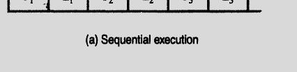
4 Single Bus Architecture


5 Input-Output Gating of the registers s in the single-bus architecture
6 Timing Diagram of a: Memory Read operation
7 Three-bus organization of datapath; Or CPU architecture
8 Data Flow (Fetch Operation) Source: Stallings
9 MIPS (Microprocessor without Interlocked Pipeline Stages) is a reduced instruction set computer (RISC) instruction ti set architecture t (ISA). Computer workstation systems using MIPS processors are: SGI, MIPS Computer Systems, Inc., Whitechapel Workstations, Olivetti, Siemens-Nixdorf, Acer, Digital Equipment Corporation, NEC, and DeskStation. Operating systems ported to the architecture include: SGI's IRIX, Microsoft's s Windows NT (until v4.0), Windows CE, Linux, BSD, UNIX System V, SINIX, QNX. The R8000 (1994) was the first superscalar MIPS design, able to execute two integer or floating point and two memory instructions per cycle. The design was spread over six chips: an integer unit (with 16 KB instruction and 16 KB data caches), a floating-point unit, three full-custom secondary cache tag RAMs (two for secondary cache accesses, one for bus snooping), and a cache controller ASIC. The design had two fully pipelined double precision multiplyadd units, which could stream data from the 4 MB off-chip secondary cache.
10 MIPS instruction set 32 general purpose registers Backwards compatible 32 bit wide (even on 64-bit processors) Load-store machine 3 categories of instructions Load-store Arithmetic and logical Jump and branch
11
12 Type -31- format (bits) -0- R opcode (6) rs (5) rt (5) rd (5) shamt (5) funct (6) I opcode (6) rs (5) rt (5) immediate (16) J opcode (6) Target Address (26) All MIPS instructions are 32 bits long. The three instruction formats: R-type (Register) I-type (Immediate) J-type (Jump) The different fields are: op: operation of the instruction (opcode) rs, rt, rd: the source and destination register specifiers shamt: shift amount (arithmetic/logical ) funct: selects ects the variant a of the operation o in the op field address / immediate: address offset or immediate value target address: target address of the jump instruction


13 Every instruction : starts with a 6-bit opcode. In addition to the opcode, R-type instructions specify three registers, a shift amount field, and a function field; I-type instructions specify two registers and a 16-bit immediate value; J-type instructions follow the opcode with a 26-bit jump target.
14 MIPS Instruction encoding reg means a register number between 0 and 31, address means a 16-bit address, and n.a. (not applicable) means this field does not appear in this format. add and sub instructions have the same value in the op field; the hardware uses the funct field to decide the variant of the operation: add (32) or subtract (34). In MIPS assembly language, registers $s0 to $s7 map onto registers 16 to 23, and registers $t0 to $t7 map onto registers 8 to 15. Hence,,$ $s0 means register 16,,$ $s1 means register 17,,$ $s2 means register 18,..., $t0 means register 8, $t1 means register 9 etc. add $t0, $s1, $s2
15 The assignment statement: A[300] = h + A[300]; is compiled into: /* <opn.> dtn, src lw $t0, 32($s3) # Temporary reg $t0 gets A[8] add $t0, $s2, $t0 # Temporary reg $t0 gets h + A[8] sw $t0, 48($s3) # Stores h + A[8] back into A[12] The Equivalent C-statement is: A[12] = h + A[8]; lw $t0, 1200($t1) # Temporary reg $t0 gets A[300] add $t0, $s2, $t0 # Temporary reg $t0 gets h + A[300] sw $t0, 1200($t1) # Stores h + A[300] back into A[300]; /* <opn.> src, dtn op rs rt rd Addr/Shamt Funct
16 MIPS Addressing Mode Summary Multiple l forms of addressing are generically called addressing modes. The MIPS addressing modes are the following: 1. Register addressing, where the operand is a register 2. Base or displacement addressing, where the operand is at the memory location, whose address is the sum of a register and a constant in the instruction 3. Immediate addressing, where the operand is a constant within the instruction itself 4. PC-relative addressing, where the address is the sum of the PC and a constant in the instruction 5. Pseudodirect addressing, where the jump address is the 26 bits of the instruction concatenated with the upper bits of the PC
17 Five MIPS addressing modes. The operands are shaded in color. The operand of mode 3 is in memory, whereas the operand for mode 2 is a register. Note that versions of load and store access bytes, halfwords, or words. For mode 1, the operand is 16 bits of the instruction itself. Modes 4 and 5 address instructions in memory, with mode 4 adding a 16-bit address shifted left 2 bits to the PC and mode 5 concatenating a 26-bit address shifted left 2 bits with the 4 upper bits of the PC.
18 sll/srl = Shift left/ right logical sll $t2, $s0, 4 # reg $t2 = reg $s0 << 4 bits 4*(2 30-1)
19
20 Addressing in Branches and Jumps j # go to location bne $s0, $s1, Exit # go to Exit, if $s0 <> $s1 A branch instruction would calculate the following: Program counter = Register + Branch address; This sum allows the program to be as large as 2 32 and still be able to use conditional branches, solving the branch address size problem. The question is then, which register? Since the program counter (PC) contains the address of the current instruction, ti we can branch within +/-(2 15 ) words of the current instruction if we use the PC as the register to be added to the address. Almost all loops and if statements are much smaller than 2 16 words, so the PC is the ideal choice. This form of branch addressing is called PC-relative addressing.
21 Addressing in Branches and Jumps Hence, the MIPS address is actually relative to the address of the following instruction (PC + 4) as opposed to the current instruction (PC). Like most recent computers, MIPS uses PC-relative addressing for all conditional branches because the destination of these instructions is likely to be close to the branch. On the other hand, jump-and-link instructions invoke procedures that have no reason to be near the call, and so they normally use other forms of addressing. Hence, the MIPS architecture offers long addresses for procedure calls by using the J-type format for both jump and jump-and-link instructions. Since all MIPS instructions are 4 bytes long, MIPS stretches the distance of the branch by having PC-relative addressing refer to the number of words to the next instruction instead of the number of bytes. Thus, the 16-bit field can branch four times as far by interpreting the field as a relative word address rather than as a relative byte address. Similarly, the 26-bit field in jump instructions is also a word address, meaning that it represents a 28-bit byte address. Since the PC is 32 bits, 4 bits must come from somewhere else. The MIPS jump instruction replaces only the lower 28 bits of the PC, leaving the upper 4 bits of the PC unchanged.
22 while (save[i] == k) /* C-code i += 1; Assume that i and k correspond to registers $s3 and $s5 and the base of the array save is in $s6. The while loop above, compiled into this MIPS assembler code: Loop: sll $t1, $s3, 2 # Temp reg $t1 = 4 * i add $t1, $t1, $s6 # $t1 = address of save[i] lw $t0, 0($t1) # Temp reg $t0 = save[i] bne $t0, $s5, Exit # go to Exit if save[i] <> k addi $s3, $s3, 1 # i = i + 1 j Loop # go to Loop Exit: If we assume we place the loop starting at location in memory, what is the MIPS machine code for this loop?
23 Loop: sll $t1, $s3, 2 # Temp reg $t1 = 4 * i add $t1, $t1, $s6 # $t1 = address of save[i] lw $t0, 0($t1) # Temp reg $t0 = save[i] bne $t0, $s5, Exit # go to Exit if save[i] <> k addi $s3, $s3, 1 # i = i + 1 j Loop # go to Loop Exit: beq $s0, $s1, L1; replace by a pair of instructions that offers a much greater branching distance L2: bne $s0, $s1, L2 j L1
24 Five MIPS addressing modes. The operands are shaded in color. The operand of mode 3 is in memory, whereas the operand for mode 2 is a register. Note that versions of load and store access bytes, halfwords, or words. For mode 1, the operand is 16 bits of the instruction itself. Modes 4 and 5 address instructions i in memory, with mode 4 adding a 16-bit address shifted left 2 bits to the PC and mode 5 concatenating a 26-bit address shifted left 2 bits with the 4 upper bits of the PC.
25 Features in a multi-cycle implementation of a MIPS processor : A single memory unit is used for both instructions and data. There is a single ALU, rather than an ALU and two adders. One or more registers are added after every major functional unit to hold the output of that unit until the value is used in a subsequent clock cycle. In this multi-cycle design, we assume that the clock cycle can accommodate at most one of the following operations: a memory access, a register file access (two reads or one write), or an ALU operation. Hence, any data produced by one of these three functional units (the memory, the register file, or the ALU) must be saved, into a temporary register for use on a later cycle. If it t d th th ibilit f ti i If it were not saved then the possibility of a timing race could occur, leading to the use of an incorrect value.
26 Source - D. A. Patterson and J. L. Hennessy, y, major functional blocks of the CPU, for multi-cycle datapath implementation of the ISA instructions (MIPS)
27 The following temporary registers are added to meet these requirements: The Instruction register (IR) and the Memory data register (MDR) are added to save the output of the memory for an instruction read and a data read, respectively. Two separate registers are used, since, both values are needed during the same clock cycle. The A and B registers are used to hold the register operand values read from the register file. The ALUOut register holds the output of the ALU. Because several functional units are shared for different purposes, use multiplexors. For example, since one memory is used for both instructions and data, we need a multiplexor to select between the two sources for a memory address, namely, the PC (for instruction access) and ALUOut (for data access).
28 A single ALU must accommodate all the inputs. Major parts of the datapath now consists of: 1. An additional multiplexor is added for the first ALU input. The multiplexor l chooses between the A register and the PC. 2. The multiplexor on the second ALU input is a 2-4 way multiplexor. The two additional inputs to the multiplexor are the constant 4 (used to increment the PC) and the sign-extended and shifted offset field (used in the branch address computation).
29 With the jump instruction and branch instruction, there are three possible sources for the value to be written into the PC: 1.The output of the ALU, which is the value PC + 4 during instruction ti fetch. This value should be stored directly into the PC. 2. The register ALUOut, which is where we will store the address of the branch target after it is computed. 3. The lower 26 bits of the Instruction register (IR) shifted left by two and concatenated with the upper 4 bits of the incremented PC, which is the source when the instruction is a jump. The PC is written both unconditionally and conditionally. During a normal increment and for jumps, the PC is written unconditionally. If the instruction is a conditional branch, the incremented PC is replaced with the value in ALUOut only if the two designated registers are equal.
30
31
32
33
34 The control function for a simple implementation is completely specified by this truth table.
35
36 Each MIPS instruction needs from three to five of these steps: 1. Instruction fetch step: Fetch the instruction from memory and compute the address of the next sequential instruction: IR <= Memory[PC]; PC <= PC + 4; 2. Instruction decode and register fetch step A <= Reg[IR[25:21]]; // Reg. rs in opcode B <= Reg[IR[20:16]]; // Reg. rt in opcode ALUOut <= PC + (sign-extend (IR[15-0]) << 2); // Branch target address 3. Execution, memory address computation, or branch completion i) Memory reference: ALUOut <= A + sign-extend (IR[15:0]); ii) Arithmetic-logical instruction (R-type): ALUOut <= A op B; iii) Branch: if (A == B) PC <= ALUOut;
37 3. Execution, memory address computation, or branch completion i) Memory reference: ALUOut <= A + sign-extend (IR[15:0]); ii) Arithmetic-logical instruction (R-type): ALUOut <= A op B; iii) Branch: if (A == B) PC <= ALUOut; iv) Jump: // {x, y} represents concatenation of bit fields x and y PC <= {PC [31:28], (IR[25:0]] <<2)}; 4. Memory access or R-type instruction completion step Memory reference: MDR <= Memory [ALUOut]; //Load or Memory [ALUOut] <= B; //Store from rt to Mem. Arithmetic-logical instruction (R-type): Reg[IR[15:11]] [ <= ALUOut; // Reg. rd in opcode 5. Memory read completion step - Load: Reg[IR[20:16]] <= MDR; // Reg. rt
38 first two steps are independent of the instruction class. After these steps, an instruction takes from one to three more cycles to complete, depending on the instruction class. In a multi-cycle implementation, a new instruction will be started as soon as the current instruction completes. The register file actually reads every cycle, but as long as the IR does not change, the values read from the register file are identical. In particular, the value read into register B during the Instruction ti decode d stage, for a branch or R-type instruction, ti is the same as the value stored into B during the Execution stage and then used in the Memory access stage for a store word instruction.
39 Remember this?? Now compare the two
40
41
42 Functions of Control Unit Sequencing Causing the CPU to step through a series of micro- operations Execution Causing the performance of each micro-op Use of Control Signals to accomplish the task
43 Types of Control Signals Clock One micro-instruction (or set of parallel microinstructions) per clock cycle o Instruction register Op-code for current instruction Determines which h micro-instructions i i are performed Flags State of CPU Results of previous operations From control bus Interrupts Acknowledgements
44 Model of Control Unit
45 HARDWIRED CONTROL The required control signals are determined by the following information: Contents of the control Step Counter Contents of the IR Contents of the condition code flags External I/P signals, MFC, IRQ etc.
46 Control Unit with Decoded Inputs
47 CLK Control Step Counter RESET STEP Decoder T 1 T 2 T n INS 1 External Inputs IR Instruction Decoder INS 2 ENCODER INS m RUN END Condition Codes CONTROL SIGNALS
48
49 For an ADD instruction (ISA): 1. PCout, MARin, READ, SEL #4, ADD, Zin MDRout, SEL Y, ADD, Zin For a Branch instruction (ISA): 1. PCout,, Zin Offset (IRout), ADD, Zin 5. Zout, PCin, END Z in T T 1 6. ADD T4. BR... END = T 7.ADD + T 5.BR + (T 5.CF + T 4.CF ).BRN +. When RUN = 0, the counter STOPS; required from W_MFC; Design logic mostly based on FSM (Finite State machine)
50 Z in T T6. ADD T4. BR... 1 END = T 7.ADD + T 5.BR + (T 5.CF + T 4.CF ).BRN +.
51 FSM based Hardware Control Unit design Moore type machine necessary - output signal depends on the current state. Next state depends on the input and current state. Each state generates a set of control signals. To implement any ISA, the system sequentially changes state from one to another. Control Unit implements the steps. For a sequence of N steps, there are S 0 to S N-1 stages. At each stage S i: a set of outputs O i,0.o i,m-1 are generated, depending on the S i. Categories of control signals: functions for ALU, select of storage units, select of data routes (based on design).
52 0 0 S S 1 1 S Typical Moore State Graph 1 S AB Moore state table A + B + X=0 X=1 Z (Present output) S S S 2 0 S S S 2 1 S S S 3 1 S S S 1 0
53 Moore network example X 1 X 2 onal Combinati Q 1 + D 1 F/F Clk Q 1 Z 1 Sub N/W for F/F inputs X m Q 2 + Q 1 Q 2 D 2 Clk F/F Q 2 Combinati -onal Sub N/W for Outputs Z 2 Z n Q k + D k F/F Q k Clk Q k Clk
54 The outputs of the combinational logic are the nextstate number and the control signals to be asserted for the current state. The inputs to the combinational logic are the current state and any inputs used to determine the next state. In this case, the inputs are the instruction register opcode bits. Notice that in the FSM for Hardwired Control, the outputs depend only on the current state, not on the inputs. Identifying i characteristic ti for a Moore machine is that t the output depends only on the current state. For a Moore machine, the box labeled combinational control logic can be split into two pieces. One piece has the control output and only the state input, while the other has only the next-state output.
55 START INSTRCN FETCH DECODE REG. FETCH MEM. ACCESS INSTRCN R-Type INSTRCN. BRANCH INSTRCN JUMP INSTRCN OVERALL state machine diagram for CPU
56 START INSTRCN. FETCH INSTRCN. DECODE/ Register FETCH MMEORY ADDRESS COMPN. EXECUTION BRANCH JUMP MEMORY ACCESS R-TYPE COMPN. WRITE BACK FSM Graph
57
58
59
60 Moore type machine - output signal depends on the current state. Next state depends on the input and current state.
61
62
63
64 Break the control function into two parts: -the next-state outputs, which depend on all the inputs, and - the control signal outputs, which depend only on the current-state bits Let s look at a ROM-based implementation, ti first.
65
66 e.g.: PCWrite is high in states 0 and 9; this corresponds to addresses with the 4 low-order bits being either 0000 or The bit will be high in the memory word independent of the inputs Op[5 0], so the addresses with the bit high are , , , ,..., , The general form of this is XXXXXX0000 or XXXXXX1001.
67 The truth table for next-state output bit (NS[0]). The next-state outputs depend on the value of Op[5 0], which is the opcode field, and the current state, given by S[3 0].
68 The four truth th tables for the four next-state output bits (NS[3 0]). The next-state outputs depend on the value of Op[5 0], which is the opcode field, and the current state, given by S[3 0].
69
70 The entry from the top yields , while the appropriate entry in the table below is Thus the control word at address is The column labeled Any other value applies only when the Op bits do not match one of the specified opcodes. For example, the word at address is obtained by finding (i) the upper 16 bits from the table on top, using only the state input bits (0001) and (ii) concatenating the lower 4 bits found by using the entire address (0001 to find address (0001 to find the row and to find the column).
71 For ALU Control & simple CPU control lines check slides: 32-35
72
73 TYPES of PLDS: PAL - PAL devices have arrays of transistor cells arranged in a "fixed-or, programmable-and" plane used to implement "sum-ofproducts" binary logic equations PLA - The PLA (also FPLA) has a set of programmable AND gate planes, which link to a set of programmable OR gate planes, which can then be conditionally complemented to produce an output. This layout allows for a large number of logic functions to be synthesized in the sum of products (and sometimes product of sums) in canonical forms. GAL - The GAL (Generic Array Logic) was an improvement on the PAL because one device was able to take the place of many PAL devices or could even have functionality not covered by the original range. Its primary benefit, however, was that it was erasable and reprogrammable making prototyping and design changes easier for engineers. A similar device called a PEEL (programmable electrically erasable logic) was introduced by the International CMOS Technology (ICT) corporation.
74 FPGA - FPGAs contain programmable logic components called "logic blocks", and a hierarchy of reconfigurable interconnects that allow the blocks to be "wired together - somewhat like a one-chip programmable breadboard. The most common FPGA architecture consists of an array of configurable logic blocks (CLBs), I/O pads, and routing channels. Generally, all the routing channels have the same width (number of wires). Multiple I/O pads may fit into the array programmable using HDL. CPLD between PALs and FPGAs. Has ROM and hence nonvolatile. Handles complex logics with feedback and arithmetic operations. ROM PLC - Automation of machinery control a small embedded system PLL??
75 Various optimizers and sequencers are used for efficient design. Difficult to design when complex operations/instructions are necessary Floating point, superscalar, pipelining etc. Correcting errors and debugging is difficult How do you implement W(MFC) in this state machine?? Minor modifications of the ISA requires lot of changes and redo the design. Complex instructions may require to go through several states and signals to be generated M d h d i i RISE l b /h ll f Many opcodes the design may require a RISE lab./hall for generating the truth table.
76 Microprogramming Micro-Instructions for: ADD (R3), R1
77
78 The PC is incremented every time a new micro- instruction is fetched from the micro-program (Control Store) memory, except in the following situations: 1. When a new instruction is loaded into the IR, the PC is loaded with the starting address of the micro- routine for that instruction. 2. When a Branch microinstruction is encountered and the branch condition is satisfied, the PC is loaded d with the branch address. 3. When an End microinstruction is encountered, the PC is loaded with the address of the first CW in the microroutine for the instruction fetch cycle (this address is 0).
79 Drawbacks of this simple micro-instrcn. system: - assigning individual bits to each control signal results in long microinstructions because the number of required signals is usually large. - only a few bits are set to 1 (for active gating) in any given microinstruction, which means the available bit space is poorly used. Assume: In total, 42 control signals are needed. e.g. - Read, Write, Select, WMFC, End; -Add, Subtract, AND, and XOR; - Separate signals to R i s ; PC, IR, MAR, MDR etc.
80 42 bits would be needed in each microinstruction. Fortunately, the length of the microinstructions can be reduced easily. Most signals are not needed simultaneously, and many signals are mutually exclusive. For example, only one function of the ALU can be activated at a time. The source for a data transfer must be unique because it is not possible to gate the contents of two different registers onto the bus at the same time. Read and Write signals to the memory cannot be active simultaneously. This suggests that signals can be grouped so that all mutually exclusive signals are placed in the same group. Thus, at most one microoperation per group is specified in any microinstruction
81 For example, four bits suffice to represent the 16 available functions in the ALU. Register output control signals can be placed in a group consisting of PC out, MDR out, Z out, Offset out, R0 out, R1 out, R2 out, R3 out and TEMP out. Thus, do this natural grouping (of mutually exclusive signals) and then - Select anyone by a 4-bit code. Most fields must include one inactive code for the case in which no action is required. Grouping control signals into fields requires a little more hardware because decoding circuits must be used to decode d the bit patterns of each field into individual id control signals. The cost of this additional hardware is more than offset by the reduced number of bits in each microinstruction, which results in a smaller CONTROL store.
82 Only 20 bits are needed to store the patterns for the 42 signals
83 VERTICAL ORGANIZATION is also possible, where compact codes are generated using highly encoded schemes. HORIZONTAL ORGANIZATION
84 MICROPROGRAM SEQUENCING Having a separate microroutine for each machine instruction results in a large total number of microinstructions and a large control store. If most machine instructions involve several addressing modes, there can be many instruction and addressing mode combinations. A separate microroutine for each of these combinations would produce considerable duplication of common parts. Its better to organize the microprogram so that the microroutines share as many common parts as possible. This requires many branch microinstructions to transfer control among the various parts. e.g. Consider an instruction of the type: Add R src, R dst Addressing modes: Addressing modes: register, autoincrement, autodecrement, and indexed, as well as the indirect forms of these four modes.
85 Address indicated by an OCTAL number; Note minor change in notation of microprogram instructions
86
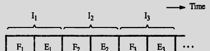
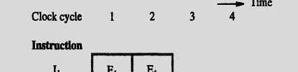
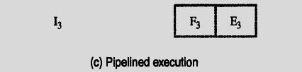
87 Branch Address Modification using Bit-ORing Consider the point labeled l in the figure. At this point, it is necessary to choose between actions required by direct and indirect addressing modes. If the indirect mode is specified in the instruction, then the microinstruction in location 170 is performed to fetch the operand from the memory. If the direct mode is specified, this fetch must be bypassed by branching immediately to location 171. The most efficient way to bypass microinstruction 170 is to have the preceding branch microinstructions specify the address 170 and then use an OR gate to change the least significant ifi bit of this address to 1 if the direct addressing mode is involved. This is known as the bit-oring technique for modifying branch addresses.
88 Wide BRANCH ADDRESSING The instruction decoder {lnstdec}, generates the starting address of the microroutine that implements the instruction that has just been loaded into the IR. In our example, register IR contains the Add instruction, for which the instruction decoder generates the micro- instruction address 101, which cannot be loaded as is into the microprogram counter ( PC). The bit-oring technique can be used at this point to modify the starting address generated by the instruction decoder to reach the appropriate path. Bit-Oring should change the address 101 to one of the five possible address values, 161, 141, 121, 101, or 111, depending on the addressing mode used in the instruction
89 Execute the instruction - Add (Rsrc)+, Rdst The instruction has a 3-bit field to specify the addressing mode for the source operand, as above. Bit patterns: 11, 10, 01, and 00, located in bits 10 and 9, denote the indexed, autodecrement, autoincrement, and register modes, respectively. For each of these modes, bit 8 is used to specify the indirect version.
90 Add (Rsrc)+, Rdst; IR 10-9 for Auto-increment mode: 01; IR 8 = 0 (no Indirect); Thus, PC 5-3 = (010) 2 = (2) 8 ; Modified PC for branching after (003) 8 = (121) 8 ; Modified PC for branching after (123) 8 = (171) 8 ; //Direct mode
91 Micro-instruction with next Address Field. <* For self-study in END SEM Exam. *>
92 The selection of the next microinstruction is controlled by the sequencing control outputs from the control logic. A typical implementation of a microcode controller The address select logic contains a set of dispatch tables as well as the logic to select from among the alternative next states. The combination of the current microprogram counter, incrementer, dispatch tables, and address select logic forms a sequencer that selects the next microinstruction.
93


94 PIPELINING Hence, 4 units of time slots used; Compared to 3*2 = 6 units of time required for a Sequential ential operation.
95 A pipelined processor may process each instruction in four steps, as follows: F Fetch: read the instruction from the memory; D Decode: decode d the instruction ti and fetch the source operand(s); E Execute: perform the operation specified by the instruction; W Write: store the result in the destination location. Here, 7 units of time slots used; Compared to 4*4 = 16 units of time required for a Sequential operation.
96
97 A Data Hazard, due to delayed EXEC cycle
98 Instruction or Control Hazard
99 An Instruction or Control Hazard, also possible due to Cache miss in W_MFC The Decode unit is idle in cycles 3 through 5, the Execute unit is idle in cycles 4 through 6, and the Write unit is idle in cycles 5 through 7. Such idle periods are called stalls. They are also often referred to as bubbles in the pipeline. Once created as a result of a delay in one of the pipeline pp stages, a bubble moves downstream until it reaches the last unit.
100 A Structural Hazard, also possible due conflict of usage of the same resource by two or more instructions
101 Data Hazard, due to concurrent instruction dependencies Assume A = 5; Concurrent execution leads to B = 20 (incorrect) Sequential execution leads to: B = 32 (Correct) No problem of concurrency in this case:
102 An Instructional Hazard, also possible due to - Branching Read: - Pre-fetching - Delayed Branch - Branch Prediction - Dispatch operation - Performance (throughput) Gain - Effect of Addressing modes - Condition codes - Datapath and Control - Superscalar CPU - Out of order execution
103 Pipelined MIPS, showing the five stages (instruction fetch, instruction decode, execute, memory access and write back
104 A superscalar CPU architecture implements a form of parallelism called instruction level parallelism within a single processor. It therefore allows faster CPU throughput than would otherwise be impossible at a given clock rate. A superscalar processor executes more than one instruction during a clock cycle by simultaneously dispatching multiple instructions to redundant functional units on the processor. Each functional unit is not a separate CPU core but an execution resource within a single CPU such as an arithmetic logic unit, a bit shifter, or a multiplier. In the Flynn Taxonomy, a superscalar processor is classified as a MIMD processor (Multiple Instructions, Multiple Data). While a superscalar CPU is typically also pipelined, pipelining and superscalar architecture t are considered d different performance enhancement techniques. The superscalar technique is traditionally associated with several identifying characteristics (within a given CPU core): Instructions are issued from a sequential instruction stream CPU hardware dynamically checks for data dependencies between instructions at run time (versus software checking at compile time) The CPU accepts multiple instructions per clock cycle
105
Basic Processing Unit: Some Fundamental Concepts, Execution of a. Complete Instruction, Multiple Bus Organization, Hard-wired Control,
 UNIT - 7 Basic Processing Unit: Some Fundamental Concepts, Execution of a Complete Instruction, Multiple Bus Organization, Hard-wired Control, Microprogrammed Control Page 178 UNIT - 7 BASIC PROCESSING
COMPUTER ORGANIZATION AND DESIGN. 5 th Edition. The Hardware/Software Interface. Chapter 4. The Processor
 COMPUTER ORGANIZATION AND DESIGN The Hardware/Software Interface 5 th Edition Chapter 4 The Processor Introduction CPU performance factors Instruction count Determined by ISA and compiler CPI and Cycle
Chapter 4. Instruction Execution. Introduction. CPU Overview. Multiplexers. Chapter 4 The Processor 1. The Processor.
 COMPUTER ORGANIZATION AND DESIGN The Hardware/Software Interface 5 th Edition COMPUTER ORGANIZATION AND DESIGN The Hardware/Software Interface 5 th Edition Chapter 4 The Processor The Processor - Introduction
COMPUTER ORGANIZATION AND DESIGN. 5 th Edition. The Hardware/Software Interface. Chapter 4. The Processor
 COMPUTER ORGANIZATION AND DESIGN The Hardware/Software Interface 5 th Edition Chapter 4 The Processor COMPUTER ORGANIZATION AND DESIGN The Hardware/Software Interface 5 th Edition The Processor - Introduction
ENE 334 Microprocessors
 ENE 334 Microprocessors Lecture 6: Datapath and Control : Dejwoot KHAWPARISUTH Adapted from Computer Organization and Design, 3 th & 4 th Edition, Patterson & Hennessy, 2005/2008, Elsevier (MK) http://webstaff.kmutt.ac.th/~dejwoot.kha/
UNIT 3 - Basic Processing Unit
 UNIT 3 - Basic Processing Unit Overview Instruction Set Processor (ISP) Central Processing Unit (CPU) A typical computing task consists of a series of steps specified by a sequence of machine instructions
Implementing the Control. Simple Questions
 Simple Questions How many cycles will it take to execute this code? lw $t2, 0($t3) lw $t3, 4($t3) beq $t2, $t3, Label add $t5, $t2, $t3 sw $t5, 8($t3) Label:... #assume not What is going on during the
Basic Processing Unit (Chapter 7)
") Basic Processing Unit (Chapter 7) IN1212-PDS 1 Problem instruction? y Decoder a ALU y f Reg IN1212-PDS 2 Basic cycle Assume an instruction occupies a single word in memory Basic cycle to be implemented:
Basic Processing Unit (Chapter 7) IN1212-PDS 1 Problem instruction? y Decoder a ALU y f Reg IN1212-PDS 2 Basic cycle Assume an instruction occupies a single word in memory Basic cycle to be implemented:
The Processor: Datapath & Control
 Chapter Five 1 The Processor: Datapath & Control We're ready to look at an implementation of the MIPS Simplified to contain only: memory-reference instructions: lw, sw arithmetic-logical instructions:
The Processing Unit. TU-Delft. in1210/01-pds 1
 The Processing Unit in1210/01-pds 1 Problem instruction? y Decoder a ALU y f Reg in1210/01-pds 2 Basic cycle! Assume an instruction occupies a single word in memory! Basic cycle to be implemented: 1. Fetch
CC 311- Computer Architecture. The Processor - Control
 CC 311- Computer Architecture The Processor - Control Control Unit Functions: Instruction code Control Unit Control Signals Select operations to be performed (ALU, read/write, etc.) Control data flow (multiplexor
Multicycle Approach. Designing MIPS Processor
 CSE 675.2: Introduction to Computer Architecture Multicycle Approach 8/8/25 Designing MIPS Processor (Multi-Cycle) Presentation H Slides by Gojko Babić and Elsevier Publishing We will be reusing functional
TDT4255 Computer Design. Lecture 4. Magnus Jahre. TDT4255 Computer Design
 1 TDT4255 Computer Design Lecture 4 Magnus Jahre 2 Outline Chapter 4.1 to 4.4 A Multi-cycle Processor Appendix D 3 Chapter 4 The Processor Acknowledgement: Slides are adapted from Morgan Kaufmann companion
Chapter 4. The Processor
 Chapter 4 The Processor Introduction CPU performance factors Instruction count Determined by ISA and compiler CPI and Cycle time Determined by CPU hardware We will examine two MIPS implementations A simplified
MC9211Computer Organization. Unit 4 Lesson 1 Processor Design
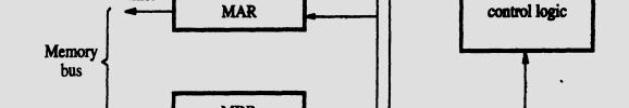
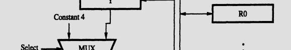
 MC92Computer Organization Unit 4 Lesson Processor Design Basic Processing Unit Connection Between the Processor and the Memory Memory MAR PC MDR R Control IR R Processo ALU R n- n general purpose registers
ECE369. Chapter 5 ECE369
 Chapter 5 1 State Elements Unclocked vs. Clocked Clocks used in synchronous logic Clocks are needed in sequential logic to decide when an element that contains state should be updated. State element 1
Topic #6. Processor Design
 Topic #6 Processor Design Major Goals! To present the single-cycle implementation and to develop the student's understanding of combinational and clocked sequential circuits and the relationship between
5.7. Microprogramming: Simplifying Control Design 5.7
 5.7 Microprogramming: Simplifying Control Design 5.7 For the of our simple MIPS subset, a graphical representation of the finite state machine, as in Figure 5.40 on page 345, is certainly adequate. We
Chapter 4 The Processor (Part 2)
") Department of Electr rical Eng ineering, Chapter 4 The Processor (Part 2) 王振傑 (Chen-Chieh Wang) ccwang@mail.ee.ncku.edu.tw ncku edu Feng-Chia Unive ersity Outline A Multicycle Implementation Mapping Control
Department of Electr rical Eng ineering, Chapter 4 The Processor (Part 2) 王振傑 (Chen-Chieh Wang) ccwang@mail.ee.ncku.edu.tw ncku edu Feng-Chia Unive ersity Outline A Multicycle Implementation Mapping Control
Chapter 4. The Processor
 Chapter 4 The Processor Introduction CPU performance factors Instruction count Determined by ISA and compiler CPI and Cycle time Determined by CPU hardware We will examine two MIPS implementations A simplified
Processor (I) - datapath & control. Hwansoo Han
 - datapath & control. Hwansoo Han") Processor (I) - datapath & control Hwansoo Han Introduction CPU performance factors Instruction count - Determined by ISA and compiler CPI and Cycle time - Determined by CPU hardware We will examine two
Processor (I) - datapath & control Hwansoo Han Introduction CPU performance factors Instruction count - Determined by ISA and compiler CPI and Cycle time - Determined by CPU hardware We will examine two
Lecture 5 and 6. ICS 152 Computer Systems Architecture. Prof. Juan Luis Aragón
 ICS 152 Computer Systems Architecture Prof. Juan Luis Aragón Lecture 5 and 6 Multicycle Implementation Introduction to Microprogramming Readings: Sections 5.4 and 5.5 1 Review of Last Lecture We have seen
Module 5 - CPU Design
 Module 5 - CPU Design Lecture 1 - Introduction to CPU The operation or task that must perform by CPU is: Fetch Instruction: The CPU reads an instruction from memory. Interpret Instruction: The instruction
Systems Architecture I
 Systems Architecture I Topics A Simple Implementation of MIPS * A Multicycle Implementation of MIPS ** *This lecture was derived from material in the text (sec. 5.1-5.3). **This lecture was derived from
Mapping Control to Hardware
 C A P P E N D I X A custom format such as this is slave to the architecture of the hardware and the instruction set it serves. The format must strike a proper compromise between ROM size, ROM-output decoding,
Chapter 4. The Processor
 Chapter 4 The Processor Introduction CPU performance factors Instruction count Determined by ISA and compiler CPI and Cycle time Determined by CPU hardware 4.1 Introduction We will examine two MIPS implementations
CPE 335. Basic MIPS Architecture Part II
 CPE 335 Computer Organization Basic MIPS Architecture Part II Dr. Iyad Jafar Adapted from Dr. Gheith Abandah slides http://www.abandah.com/gheith/courses/cpe335_s08/index.html CPE232 Basic MIPS Architecture
CISC 662 Graduate Computer Architecture. Lecture 4 - ISA
 CISC 662 Graduate Computer Architecture Lecture 4 - ISA Michela Taufer http://www.cis.udel.edu/~taufer/courses Powerpoint Lecture Notes from John Hennessy and David Patterson s: Computer Architecture,
ELEC 5200/6200 Computer Architecture and Design Spring 2017 Lecture 4: Datapath and Control
 ELEC 52/62 Computer Architecture and Design Spring 217 Lecture 4: Datapath and Control Ujjwal Guin, Assistant Professor Department of Electrical and Computer Engineering Auburn University, Auburn, AL 36849
The Processor: Datapath and Control. Jin-Soo Kim Computer Systems Laboratory Sungkyunkwan University
 The Processor: Datapath and Control Jin-Soo Kim (jinsookim@skku.edu) Computer Systems Laboratory Sungkyunkwan University http://csl.skku.edu Introduction CPU performance factors Instruction count Determined
Chapter 4. The Processor. Instruction count Determined by ISA and compiler. We will examine two MIPS implementations
 Chapter 4 The Processor Part I Introduction CPU performance factors Instruction count Determined by ISA and compiler CPI and Cycle time Determined by CPU hardware We will examine two MIPS implementations
Chapter 4. The Processor
 Chapter 4 The Processor Introduction CPU performance factors Instruction count Determined by ISA and compiler CPI and Cycle time Determined by CPU hardware We will examine two MIPS implementations A simplified
Introduction. ENG3380 Computer Organization and Architecture MIPS: Data Path Design Part 3. Topics. References. School of Engineering 1
 ENG8 Computer Organization and rchitecture MIPS: Data Path Design Part Winter 7 S. reibi School of Engineering University of Guelph Introduction Topics uilding a Complete Data Path for MIPS Multi Cycle
CISC 662 Graduate Computer Architecture. Lecture 4 - ISA MIPS ISA. In a CPU. (vonneumann) Processor Organization
 Processor Organization") CISC 662 Graduate Computer Architecture Lecture 4 - ISA MIPS ISA Michela Taufer http://www.cis.udel.edu/~taufer/courses Powerpoint Lecture Notes from John Hennessy and David Patterson s: Computer Architecture,
CISC 662 Graduate Computer Architecture Lecture 4 - ISA MIPS ISA Michela Taufer http://www.cis.udel.edu/~taufer/courses Powerpoint Lecture Notes from John Hennessy and David Patterson s: Computer Architecture,
PROBLEMS. 7.1 Why is the Wait-for-Memory-Function-Completed step needed when reading from or writing to the main memory?
 446 CHAPTER 7 BASIC PROCESSING UNIT (Corrisponde al cap. 10 - Struttura del processore) PROBLEMS 7.1 Why is the Wait-for-Memory-Function-Completed step needed when reading from or writing to the main memory?
Week 4: Assignment Solutions
 Week 4: Assignment Solutions 1. Which of the following statements are true for horizontal microinstruction encoding? a. If there are kcontrol signals, every control word stored in control memory (CM) consists
Computer Science 324 Computer Architecture Mount Holyoke College Fall Topic Notes: Data Paths and Microprogramming
 Computer Science 324 Computer Architecture Mount Holyoke College Fall 2007 Topic Notes: Data Paths and Microprogramming We have spent time looking at the MIPS instruction set architecture and building
RISC Processor Design
 RISC Processor Design Single Cycle Implementation - MIPS Virendra Singh Indian Institute of Science Bangalore virendra@computer.org Lecture 13 SE-273: Processor Design Feb 07, 2011 SE-273@SERC 1 Courtesy:
Lets Build a Processor
 Lets Build a Processor Almost ready to move into chapter 5 and start building a processor First, let s review Boolean Logic and build the ALU we ll need (Material from Appendix B) operation a 32 ALU result
Lecture 11: Control Unit and Instruction Encoding
 CSCI25 Computer Organization Lecture : Control Unit and Instruction Encoding Ming-Chang YANG mcyang@cse.cuhk.edu.hk Reading: Chap. 7.4~7.5 (5 th Ed.) Recall: Components of a Processor Register file: a
COMPUTER ORGANIZATION AND DESIGN
 COMPUTER ORGANIZATION AND DESIGN 5 Edition th The Hardware/Software Interface Chapter 4 The Processor 4.1 Introduction Introduction CPU performance factors Instruction count CPI and Cycle time Determined
Systems Architecture
 Systems Architecture Lecture 15: A Simple Implementation of MIPS Jeremy R. Johnson Anatole D. Ruslanov William M. Mongan Some or all figures from Computer Organization and Design: The Hardware/Software
Computer Architecture
 CS3350B Computer Architecture Winter 2015 Lecture 4.2: MIPS ISA -- Instruction Representation Marc Moreno Maza www.csd.uwo.ca/courses/cs3350b [Adapted from lectures on Computer Organization and Design,
Chapter 4. The Processor Designing the datapath
 Chapter 4 The Processor Designing the datapath Introduction CPU performance determined by Instruction Count Clock Cycles per Instruction (CPI) and Cycle time Determined by Instruction Set Architecure (ISA)
COMPUTER ORGANIZATION AND DESIGN The Hardware/Software Interface. 5 th. Edition. Chapter 4. The Processor
 COMPUTER ORGANIZATION AND DESIGN The Hardware/Software Interface 5 th Edition Chapter 4 The Processor Introduction CPU performance factors Instruction count Determined by ISA and compiler CPI and Cycle
The Processor. Z. Jerry Shi Department of Computer Science and Engineering University of Connecticut. CSE3666: Introduction to Computer Architecture
 The Processor Z. Jerry Shi Department of Computer Science and Engineering University of Connecticut CSE3666: Introduction to Computer Architecture Introduction CPU performance factors Instruction count
Digital System Design Using Verilog. - Processing Unit Design
 Digital System Design Using Verilog - Processing Unit Design 1.1 CPU BASICS A typical CPU has three major components: (1) Register set, (2) Arithmetic logic unit (ALU), and (3) Control unit (CU) The register
Chapter 4. The Processor. Computer Architecture and IC Design Lab
 Chapter 4 The Processor Introduction CPU performance factors CPI Clock Cycle Time Instruction count Determined by ISA and compiler CPI and Cycle time Determined by CPU hardware We will examine two MIPS
Computer Science 324 Computer Architecture Mount Holyoke College Fall Topic Notes: MIPS Instruction Set Architecture
 Computer Science 324 Computer Architecture Mount Holyoke College Fall 2009 Topic Notes: MIPS Instruction Set Architecture vonneumann Architecture Modern computers use the vonneumann architecture. Idea:
ECE 15B Computer Organization Spring 2011
 ECE 15B Computer Organization Spring 2011 Dmitri Strukov Partially adapted from Computer Organization and Design, 4 th edition, Patterson and Hennessy, Agenda Instruction formats Addressing modes Advanced
Computer Logic II CCE 2010
 Computer Logic II CCE 2010 Dr. Owen Casha Computer Logic II 1 The Processing Unit Computer Logic II 2 The Processing Unit In its simplest form, a computer has one unit that executes program instructions.
 Part A Questions 1. What is an ISP? ISP stands for Instruction Set Processor. This unit is simply called as processor which executes machine instruction and coordinates the activities of other units..
Lecture Topics. Announcements. Today: Single-Cycle Processors (P&H ) Next: continued. Milestone #3 (due 2/9) Milestone #4 (due 2/23)
 Next: continued. Milestone #3 (due 2/9) Milestone #4 (due 2/23)") Lecture Topics Today: Single-Cycle Processors (P&H 4.1-4.4) Next: continued 1 Announcements Milestone #3 (due 2/9) Milestone #4 (due 2/23) Exam #1 (Wednesday, 2/15) 2 1 Exam #1 Wednesday, 2/15 (3:00-4:20
Lecture Topics Today: Single-Cycle Processors (P&H 4.1-4.4) Next: continued 1 Announcements Milestone #3 (due 2/9) Milestone #4 (due 2/23) Exam #1 (Wednesday, 2/15) 2 1 Exam #1 Wednesday, 2/15 (3:00-4:20
CS/COE0447: Computer Organization
 CS/COE0447: Computer Organization and Assembly Language Datapath and Control Sangyeun Cho Dept. of Computer Science A simple MIPS We will design a simple MIPS processor that supports a small instruction
CS/COE0447: Computer Organization
 A simple MIPS CS/COE447: Computer Organization and Assembly Language Datapath and Control Sangyeun Cho Dept. of Computer Science We will design a simple MIPS processor that supports a small instruction
Chapter 4 The Processor 1. Chapter 4A. The Processor
 Chapter 4 The Processor 1 Chapter 4A The Processor Chapter 4 The Processor 2 Introduction CPU performance factors Instruction count Determined by ISA and compiler CPI and Cycle time Determined by CPU hardware
Introduction to CPU Design
 ١ Introduction to CPU Design Computer Organization & Assembly Language Programming Dr Adnan Gutub aagutub at uqu.edu.sa [Adapted from slides of Dr. Kip Irvine: Assembly Language for Intel-Based Computers]
Lecture 5: The Processor
 Lecture 5: The Processor CSCE 26 Computer Organization Instructor: Saraju P. ohanty, Ph. D. NOTE: The figures, text etc included in slides are borrowed from various books, websites, authors pages, and
Unsigned Binary Integers
 Unsigned Binary Integers Given an n-bit number x x n 1 n 2 1 0 n 12 xn 22 x12 x02 Range: 0 to +2 n 1 Example 2.4 Signed and Unsigned Numbers 0000 0000 0000 0000 0000 0000 0000 1011 2 = 0 + + 1 2 3 + 0
Unsigned Binary Integers
 Unsigned Binary Integers Given an n-bit number x x n 1 n 2 1 0 n 12 xn 22 x12 x02 Range: 0 to +2 n 1 Example 2.4 Signed and Unsigned Numbers 0000 0000 0000 0000 0000 0000 0000 1011 2 = 0 + + 1 2 3 + 0
CPU Organization (Design)
") ISA Requirements CPU Organization (Design) Datapath Design: Capabilities & performance characteristics of principal Functional Units (FUs) needed by ISA instructions (e.g., Registers, ALU, Shifters, Logic
ISA Requirements CPU Organization (Design) Datapath Design: Capabilities & performance characteristics of principal Functional Units (FUs) needed by ISA instructions (e.g., Registers, ALU, Shifters, Logic
Lecture 3: The Processor (Chapter 4 of textbook) Chapter 4.1
 Chapter 4.1") Lecture 3: The Processor (Chapter 4 of textbook) Chapter 4.1 Introduction Chapter 4.1 Chapter 4.2 Review: MIPS (RISC) Design Principles Simplicity favors regularity fixed size instructions small number
Lecture 3: The Processor (Chapter 4 of textbook) Chapter 4.1 Introduction Chapter 4.1 Chapter 4.2 Review: MIPS (RISC) Design Principles Simplicity favors regularity fixed size instructions small number
PESIT Bangalore South Campus
 INTERNAL ASSESSMENT TEST III Date : 21/11/2017 Max Marks : 40 Subject & Code : Computer Organization (15CS34) Semester : III (A & B) Name of the faculty: Mrs. Sharmila Banu Time : 11.30 am 1.00 pm Answer
These actions may use different parts of the CPU. Pipelining is when the parts run simultaneously on different instructions.
 MIPS Pipe Line 2 Introduction Pipelining To complete an instruction a computer needs to perform a number of actions. These actions may use different parts of the CPU. Pipelining is when the parts run simultaneously
ﻪﺘﻓﺮﺸﻴﭘ ﺮﺗﻮﻴﭙﻣﺎﻛ يرﺎﻤﻌﻣ MIPS يرﺎﻤﻌﻣ data path and ontrol control
 معماري كامپيوتر پيشرفته معماري MIPS data path and control abbasi@basu.ac.ir Topics Building a datapath support a subset of the MIPS-I instruction-set A single cycle processor datapath all instruction actions
Processing Unit CS206T
 Processing Unit CS206T Microprocessors The density of elements on processor chips continued to rise More and more elements were placed on each chip so that fewer and fewer chips were needed to construct
Note- E~ S. \3 \S U\e. ~ ~s ~. 4. \\ o~ (fw' \i<.t. (~e., 3\0)
") 5.4 A Multicycle Implementation 377 Similarly, if we had a machine with more powerful operations and addressing modes, instructions could vary from three or four functional unit delays to tens or even
5.4 A Multicycle Implementation 377 Similarly, if we had a machine with more powerful operations and addressing modes, instructions could vary from three or four functional unit delays to tens or even
2 MARKS Q&A 1 KNREDDY UNIT-I
 2 MARKS Q&A 1 KNREDDY UNIT-I 1. What is bus; list the different types of buses with its function. A group of lines that serves as a connecting path for several devices is called a bus; TYPES: ADDRESS BUS,
Multicycle conclusion
 Multicycle conclusion The last few lectures covered a lot of material! We introduced a multicycle datapath, where different instructions take different numbers of cycles to execute. A multicycle unit is
Micro-programmed Control Ch 15
 Micro-programmed Control Ch 15 Micro-instructions Micro-programmed Control Unit Sequencing Execution Characteristics 1 Hardwired Control (4) Complex Fast Difficult to design Difficult to modify Lots of
Machine Instructions vs. Micro-instructions. Micro-programmed Control Ch 15. Machine Instructions vs. Micro-instructions (2) Hardwired Control (4)
 Hardwired Control (4)") Micro-programmed Control Ch 15 Micro-instructions Micro-programmed Control Unit Sequencing Execution Characteristics 1 Machine Instructions vs. Micro-instructions Memory execution unit CPU control memory
Micro-programmed Control Ch 15 Micro-instructions Micro-programmed Control Unit Sequencing Execution Characteristics 1 Machine Instructions vs. Micro-instructions Memory execution unit CPU control memory
(1) Using a different mapping scheme will reduce which type of cache miss? (1) Which type of cache miss can be reduced by using longer lines?
 Using a different mapping scheme will reduce which type of cache miss? (1) Which type of cache miss can be reduced by using longer lines?") (1) Give a one-word definition of coherence. (1) Give a one-word definition of consistency. (1) Using a different mapping scheme will reduce which type of cache miss? (1) Which type of cache miss can be
(1) Give a one-word definition of coherence. (1) Give a one-word definition of consistency. (1) Using a different mapping scheme will reduce which type of cache miss? (1) Which type of cache miss can be
Micro-programmed Control Ch 15
 Micro-programmed Control Ch 15 Micro-instructions Micro-programmed Control Unit Sequencing Execution Characteristics 1 Hardwired Control (4) Complex Fast Difficult to design Difficult to modify Lots of
Math 230 Assembly Programming (AKA Computer Organization) Spring MIPS Intro
 Spring MIPS Intro") Math 230 Assembly Programming (AKA Computer Organization) Spring 2008 MIPS Intro Adapted from slides developed for: Mary J. Irwin PSU CSE331 Dave Patterson s UCB CS152 M230 L09.1 Smith Spring 2008 MIPS
Math 230 Assembly Programming (AKA Computer Organization) Spring 2008 MIPS Intro Adapted from slides developed for: Mary J. Irwin PSU CSE331 Dave Patterson s UCB CS152 M230 L09.1 Smith Spring 2008 MIPS
Block diagram view. Datapath = functional units + registers
 Computer design an application of digital logic design procedures Computer = processing unit + memory system Processing unit = control + datapath Control = finite state machine inputs = machine instruction,
The register set differs from one computer architecture to another. It is usually a combination of general-purpose and special purpose registers
 Part (6) CPU BASICS A typical CPU has three major components: 1- register set, 2- arithmetic logic unit (ALU), 3- control unit (CU). The figure below shows the internal structure of the CPU. The CPU fetches
CSEE 3827: Fundamentals of Computer Systems
 CSEE 3827: Fundamentals of Computer Systems Lecture 15 April 1, 2009 martha@cs.columbia.edu and the rest of the semester Source code (e.g., *.java, *.c) (software) Compiler MIPS instruction set architecture
Microprogrammed Control Approach
 Microprogrammed Control Approach Considering the FSM for our MIPS subset has 10 states, the complete MIPS instruction set, which contains more than 100 instructions, and considering that these instructions
Chapter 5: The Processor: Datapath and Control
 Chapter 5: The Processor: Datapath and Control Overview Logic Design Conventions Building a Datapath and Control Unit Different Implementations of MIPS instruction set A simple implementation of a processor
EECE 417 Computer Systems Architecture
 EECE 417 Computer Systems Architecture Department of Electrical and Computer Engineering Howard University Charles Kim Spring 2007 1 Computer Organization and Design (3 rd Ed) -The Hardware/Software Interface
Topic Notes: MIPS Instruction Set Architecture
 Computer Science 220 Assembly Language & Comp. Architecture Siena College Fall 2011 Topic Notes: MIPS Instruction Set Architecture vonneumann Architecture Modern computers use the vonneumann architecture.
The Processor (1) Jinkyu Jeong Computer Systems Laboratory Sungkyunkwan University
 Jinkyu Jeong Computer Systems Laboratory Sungkyunkwan University") The Processor (1) Jinkyu Jeong (jinkyu@skku.edu) Computer Systems Laboratory Sungkyunkwan University http://csl.skku.edu EEE3050: Theory on Computer Architectures, Spring 2017, Jinkyu Jeong (jinkyu@skku.edu)
The Processor (1) Jinkyu Jeong (jinkyu@skku.edu) Computer Systems Laboratory Sungkyunkwan University http://csl.skku.edu EEE3050: Theory on Computer Architectures, Spring 2017, Jinkyu Jeong (jinkyu@skku.edu)
LECTURE 3: THE PROCESSOR
 LECTURE 3: THE PROCESSOR Abridged version of Patterson & Hennessy (2013):Ch.4 Introduction CPU performance factors Instruction count Determined by ISA and compiler CPI and Cycle time Determined by CPU
Introduction. Datapath Basics
 Introduction CPU performance factors - Instruction count; determined by ISA and compiler - CPI and Cycle time; determined by CPU hardware 1 We will examine a simplified MIPS implementation in this course
CS31001 COMPUTER ORGANIZATION AND ARCHITECTURE. Debdeep Mukhopadhyay, CSE, IIT Kharagpur. Instructions and Addressing
 CS31001 COMPUTER ORGANIZATION AND ARCHITECTURE Debdeep Mukhopadhyay, CSE, IIT Kharagpur Instructions and Addressing 1 ISA vs. Microarchitecture An ISA or Instruction Set Architecture describes the aspects
Review: Abstract Implementation View
 Review: Abstract Implementation View Split memory (Harvard) model - single cycle operation Simplified to contain only the instructions: memory-reference instructions: lw, sw arithmetic-logical instructions:
CO Computer Architecture and Programming Languages CAPL. Lecture 18 & 19
 CO2-3224 Computer Architecture and Programming Languages CAPL Lecture 8 & 9 Dr. Kinga Lipskoch Fall 27 Single Cycle Disadvantages & Advantages Uses the clock cycle inefficiently the clock cycle must be
CSE140: Components and Design Techniques for Digital Systems
 CSE4: Components and Design Techniques for Digital Systems Tajana Simunic Rosing Announcements and Outline Check webct grades, make sure everything is there and is correct Pick up graded d homework at
The MIPS Processor Datapath
 The MIPS Processor Datapath Module Outline MIPS datapath implementation Register File, Instruction memory, Data memory Instruction interpretation and execution. Combinational control Assignment: Datapath
Initial Representation Finite State Diagram. Logic Representation Logic Equations
 Control Implementation Alternatives Control may be designed using one of several initial representations. The choice of sequence control, and how logic is represented, can then be determined independently;
Advanced Parallel Architecture Lesson 3. Annalisa Massini /2015
 Advanced Parallel Architecture Lesson 3 Annalisa Massini - 2014/2015 Von Neumann Architecture 2 Summary of the traditional computer architecture: Von Neumann architecture http://williamstallings.com/coa/coa7e.html
Mark Redekopp and Gandhi Puvvada, All rights reserved. EE 357 Unit 15. Single-Cycle CPU Datapath and Control
 EE 37 Unit Single-Cycle CPU path and Control CPU Organization Scope We will build a CPU to implement our subset of the MIPS ISA Memory Reference Instructions: Load Word (LW) Store Word (SW) Arithmetic
Micro-programmed Control Ch 17
 Micro-programmed Control Ch 17 Micro-instructions Micro-programmed Control Unit Sequencing Execution Characteristics Course Summary 1 Hardwired Control (4) Complex Fast Difficult to design Difficult to
CENG 3420 Lecture 06: Datapath
 CENG 342 Lecture 6: Datapath Bei Yu byu@cse.cuhk.edu.hk CENG342 L6. Spring 27 The Processor: Datapath & Control q We're ready to look at an implementation of the MIPS q Simplified to contain only: memory-reference
Computer Science 324 Computer Architecture Mount Holyoke College Fall Topic Notes: MIPS Instruction Set Architecture
 Computer Science 324 Computer Architecture Mount Holyoke College Fall 2007 Topic Notes: MIPS Instruction Set Architecture vonneumann Architecture Modern computers use the vonneumann architecture. Idea:
Hardwired Control (4) Micro-programmed Control Ch 17. Micro-programmed Control (3) Machine Instructions vs. Micro-instructions
 Micro-programmed Control Ch 17. Micro-programmed Control (3) Machine Instructions vs. Micro-instructions") Micro-programmed Control Ch 17 Micro-instructions Micro-programmed Control Unit Sequencing Execution Characteristics Course Summary Hardwired Control (4) Complex Fast Difficult to design Difficult to modify
Micro-programmed Control Ch 17 Micro-instructions Micro-programmed Control Unit Sequencing Execution Characteristics Course Summary Hardwired Control (4) Complex Fast Difficult to design Difficult to modify
LECTURE 6. Multi-Cycle Datapath and Control
 LECTURE 6 Multi-Cycle Datapath and Control SINGLE-CYCLE IMPLEMENTATION As we ve seen, single-cycle implementation, although easy to implement, could potentially be very inefficient. In single-cycle, we
Rui Wang, Assistant professor Dept. of Information and Communication Tongji University.
 Instructions: ti Language of the Computer Rui Wang, Assistant professor Dept. of Information and Communication Tongji University it Email: ruiwang@tongji.edu.cn Computer Hierarchy Levels Language understood
CENG 3420 Computer Organization and Design. Lecture 06: MIPS Processor - I. Bei Yu
 CENG 342 Computer Organization and Design Lecture 6: MIPS Processor - I Bei Yu CEG342 L6. Spring 26 The Processor: Datapath & Control q We're ready to look at an implementation of the MIPS q Simplified
Chapter 2A Instructions: Language of the Computer
 Chapter 2A Instructions: Language of the Computer Copyright 2009 Elsevier, Inc. All rights reserved. Instruction Set The repertoire of instructions of a computer Different computers have different instruction