Alfred Sargezi & Zain Ali. AMS Group - San Jose State University ams.sjsu.edu
|
|
|
- Spencer Collin McDonald
- 6 years ago
- Views:
Transcription
1 Cadence Inverter Transistor Sizing Tutorial Cadence Inverter Ocean Introduction Cadence Inverter Corners Tutorial Cadence Inverter VerilogA Tutorial Cadence Inverter Vout vs Vin Tutorial Alfred Sargezi & Zain Ali AMS Group - San Jose State University ams.sjsu.edu

2 Unix account and Cadence Setup Instructions 1. Set up a Unix account by visiting the following website Complete the Cadence Tutorial. This will setup cadence on your account and provide you with a general idea on how to use cadence. Type "csh" in linux terminal to switch to your directory. Alternatively, you can also go to your unix account management online and set it up as csh there.

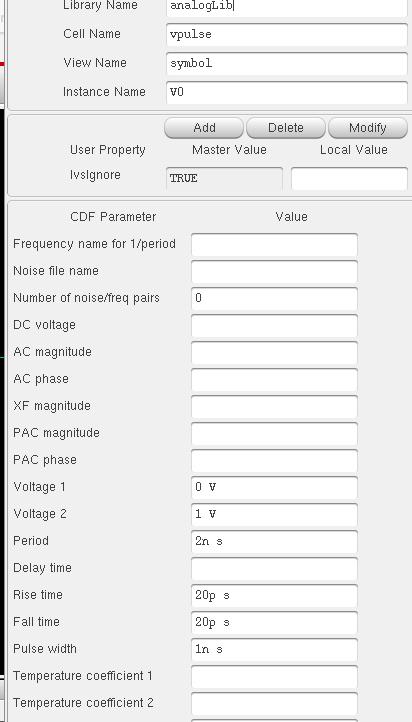
3 Testbench 1. Create a Inverter Testbench as follows: 2. Vpulse is created as follows:
4


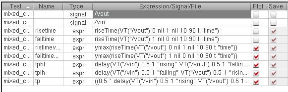
5 3. Launch ADE L and set up the following: 4. Run the ADE L once and launch calculator. Set up the following two test benches for tplh and tphl. We will be using the delay function in calculator. tplh


6 Switch rising and falling. To find tp, average them both. 5. Run a parametric analysis sweeping the width. In ADE L, under Tool select Parametric Analysis. 6. After the parametric analysis is complete, go back to calculator and plot the functions to find the optimal size for your transistors. 7. You can also use risetime and falltime to get the correct width value. We have to use the ymax function so we can extract a value since rise time and falltime are continuous functions in cadence. See below.
7
 and modify some files to get desired results instead of recreating the whole test bench. The following uses XL. 9.")
8 OCEAN and ADE XL 8. Ocean. Lets say you want to use a different transistor for whatever reason and want to finds its sizing. We can simply save a couple of scripts(inside ADE L and XL) and modify some files to get desired results instead of recreating the whole test bench. The following uses XL. 9. Start by opening up ADE XL and setting up a test bench inside it. Select Create New View and press OK. 10. Underneath data view you will see a couple of options.


9 11. Click and click to add test and it will open a window similar to ADE L.

 in the main virtuoso window and hit enter.")
10 12. This is very similar to L. Set up the test bench similar to what you did before. Run a transient analysis and select outputs and rise times, fall times, delays, etc. Leave width blank. 13. Under global variables in Data View you can add width. You can either set it up as a single value or run a sweep for certain variables. 14. ADE XL is much easier for running parametric analysis. Next we will save an ocean script. 15. You can either click on File Save script or Click on the Save script icon ( ) next to the normal button on the toolbar. Next step is to run the ocean script. The default directory will be the st45 folder where you./s45 script to start virtuoso is located. 16. To run the ocean script simply type load( size.ocn ) in the main virtuoso window and hit enter. Be patient, it will take a while to run depending on your sweep size.

11 17. If the plot window keeps closing go back to your ocean script. At the end there is a End XL Mode command section. Just comment ocnxlendxlmode() by pulling a semicolon in front of it. Rerun the ocean file and it won t close the plot anymore. 18. Once you have the plot you can figure out what the correct width ratio is. 19. Make a new schematic and name it inv_lowvt. Copy and paste the original components and simply change the transistors with pmos1v_lvt and nmos1v_lvt. Keep everything else the same. 20. Make a copy of size.ocn and name is size_lvt.ocn. Open it with a text editor (such as gedit) and replace all instances of inv with inv_lowvt. Run file size_lvt.ocn and it will plot the data with lowvt transistors. You can repeat the above steps with highvt and whatever else is in your library. 21. Note: This is just a proof of concept. If you are more comfortable with the ADE L/XL environment, just use that. This might help people process some information slightly faster. If you are interested in ocean just google a manual and look up functions.
. 23. You will get the following window.")

12 Corners 22. Corners: Under data view select Click to add corner. (If you are using ADE L then look under setup and then model libraries and you can do the same thing). 23. You will get the following window. Temperature is a predefined variable in Virtuoso. You can simply enter values. We are testing from -40 to 125. It s in degrees Celsius. You can also add parameters and design variables and sweep them here. 24. Under Model Group Select Click to edit. You will get the following window. Select Click to add. It might take a little while to load. Do not Click on the little explore button. Make sure you click on Click to add.


13 25. Mirror it to the image below. You can just type it in once and copy paste the model path. Make sure red arrow is selected and you should see a drop down menu. Add six of these so you can add all the different corners as shown below. Hit Ok.


14 26. It is very important you add all the names one by one. So for TT click on add/update after selecting it. Repeat for FF, SS and so on. 27. Once you add all of them you can see a dropdown menu Now go back to your Corner setup window. In the Model Group under Section you will see the 6 models if you set it up properly. Add all 6 of them one by one.
 and you should get something similar to this. 29.")

15 28. Now that temperature and Models are added simply hit the Add/Update Corner button(it s the red one below) and you should get something similar to this. 29. Save your sweep file using the Save button. Next time you need to run a corner analysis, simply reload the file and you can skip all of the above steps. 30. Go back to data view and make sure corner is selected.
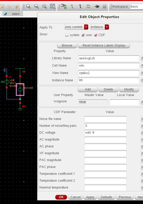
16 31. Make sure you only have one value for width. Rerun the simulation. If you sweep width again it will simply run 36*(number of widths) that you sweep. It will give you your rise and fall times for various corners. 32. Change the main power supply in the schematic and just call it vdd instead of 1V.
17

18 33. In Corners, under design variables, now select vdd and enter values 0.9, 1, Re-run the simulation. Now you will have your voltage corners too. You can vary the numbers as required. Just keep it mind, each variation adds 36 tests already in there. Modify the test bench for faster results.
 36. Create a new file. Use the following template. Save it in the same library as your inverter.")
19 Verilog - A 35. In the main virtuoso window type in editor = gedit and press enter. This will change the editor to gedit. (If you really like to use vi, you can skip this step. If you don t know what vi is, then just change your editor to gedit) 36. Create a new file. Use the following template. Save it in the same library as your inverter. We are basically making a veriloga file. It will open with gedit (if you set it up correctly). Name the file inv_veriloga. If you name it the same as your inverter you will not be able to create a symbol. 37. Write your Verilog code. If you did it properly, it will ask you to create a symbol. Else if will give you syntax errors. Sample code is below. // VerilogA for mixed_components, inv_veriloga, veriloga `include "constants.vams" `include "disciplines.vams" module inv_veriloga(in,out, vss, vdd); inout vdd, vss; input in; output out;
 and actual transistor level implementation. 40.")
20 electrical in, out, vss, vdd; analog begin if(v(in)>((v(vdd)-v(vss))/2)) V(out)<+ V(vss); else V(out)<+ V(vdd); end endmodule 38. Put everything in the same inverter test bench. 39. In ADE, plot the vin, vout and voutv. You can see the difference between an ideal model (veriloga) and actual transistor level implementation. 40. VerilogA becomes more useful when you are trying to implement complex systems. You might need to model it in varying ways depending on your output requirement.


21 Vout vs Vin + PVT 41. Copy and paste the inverter symbol one more time. Also add a DC source and declare it as a variable. I named my input dc souce as vcd, and changed input to the inverter to vcdin and output to outdc. 42. Declare the vdc as 1 under global variables and then select your corners to run.


22 43. Choose the analysis under DC analysis under tests in ADE XL. 44. Add the outputs vdcin and outdc to your results window. 45. In calculator, select the cross function. Subtract input from output to get the crossing point. cross((vs("/outdc") - VS("/vindc")) 0 1 "either" nil nil)

.")
23 46. Add the cross time equation to outputs. 47. Run the simulation. (Note: My run does not have all process corners). Should see something like this.

24 48. You will recieve plots of Vout vs Vin and then points of crossing for the Vin vs PVT. You can changes axes on the graph or extract data and plot in Matlab.
Cadence Inverter Transistor Sizing Tutorial Cadence Inverter Ocean Introduction Cadence Inverter Corners Tutorial Cadence Inverter VerilogA Tutorial
 Cadence Inverter Transistor Sizing Tutorial Cadence Inverter Ocean Introduction Cadence Inverter Corners Tutorial Cadence Inverter VerilogA Tutorial Alfred Sargezi & Zain Ali AMS Group - San Jose State
S Exercise 1C Testing the Ring Oscillator
 S-87.3148 Exercise 1C Testing the Ring Oscillator Aalto University School of Electrical Engineering Department of Micro- and Nanosciences (ECDL) 10.9.2014 1 1 Building the test bench In this exercise,
AMS 0.18 µm PDK Setup and Cadence Tutorial Contributors
 AMS 0.18 µm PDK Setup and Cadence Tutorial Contributors Muhammad Ahmed, Sita Asar, and Ayman Fayed, Power Management Research Lab, https://pmrl.osu.edu, Department of Electrical and Computer Engineering,
Cadence Tutorial A: Schematic Entry and Functional Simulation Created for the MSU VLSI program by Andrew Mason and the AMSaC lab group.
 Cadence Tutorial A: Schematic Entry and Functional Simulation Created for the MSU VLSI program by Andrew Mason and the AMSaC lab group. Revision Notes: Aug. 2003 update and edit A. Mason add intro/revision/contents
CPE/EE 427, CPE 527, VLSI Design I: Tutorial #2, Schematic Capture, DC Analysis, Transient Analysis (Inverter, NAND2)
") CPE/EE 427, CPE 527, VLSI Design I: Tutorial #2, Schematic Capture, DC Analysis, Transient Analysis (Inverter, NAND2) Joel Wilder, Aleksandar Milenkovic, ECE Dept., The University of Alabama in Huntsville
CPE/EE 427, CPE 527, VLSI Design I: Tutorial #2, Schematic Capture, DC Analysis, Transient Analysis (Inverter, NAND2) Joel Wilder, Aleksandar Milenkovic, ECE Dept., The University of Alabama in Huntsville
Revision Notes: July2004 Generate tutorial for single transistor analysis. Based on existing schematic entry tutorial developed for ECE410
 Cadence Analog Tutorial 1: Schematic Entry and Transistor Characterization Created for the MSU VLSI program by Professor A. Mason and the AMSaC lab group. Revision Notes: July2004 Generate tutorial for
The original document link is
 Tutorial:Analog Artist with HSPICE The original document link is http://www.eda.ncsu.edu/wiki/tutorial:analog_artist_with_hspice This tutorial will introduce you to the Cadence Environment: specifically
Cadence Tutorial. Introduction to Cadence 0.18um, Implementation and Simulation of an inverter. A. Moradi, A. Miled et M. Sawan
 Cadence Tutorial Introduction to Cadence 0.18um, Implementation and Simulation of an inverter A. Moradi, A. Miled et M. Sawan Section 1: Introduction to Cadence You will see how to create a new library
EE 330 Spring Laboratory 2: Basic Boolean Circuits
 EE 330 Spring 2013 Laboratory 2: Basic Boolean Circuits Objective: The objective of this experiment is to investigate methods for evaluating the performance of Boolean circuits. Emphasis will be placed
ESE 570 Cadence Lab Assignment 2: Introduction to Spectre, Manual Layout Drawing and Post Layout Simulation (PLS)
") ESE 570 Cadence Lab Assignment 2: Introduction to Spectre, Manual Layout Drawing and Post Layout Simulation (PLS) Objective Part A: To become acquainted with Spectre (or HSpice) by simulating an inverter,
ESE 570 Cadence Lab Assignment 2: Introduction to Spectre, Manual Layout Drawing and Post Layout Simulation (PLS) Objective Part A: To become acquainted with Spectre (or HSpice) by simulating an inverter,
EE115C Digital Electronic Circuits. Tutorial 2: Hierarchical Schematic and Simulation
 EE115C Digital Electronic Circuits Tutorial 2: Hierarchical Schematic and Simulation The objectives are to become familiar with Virtuoso schematic editor, learn how to create the symbol view of basic primitives,
Simulation with Verilog-XL
 Simulation with Verilog-XL Adapted from Princeton Cadence Page (http://www.ee.princeton.edu/~cadence/usr/verilog.html) Until now, we have been using the Analog Environment to do simulations. This simulator
Figure 1: ADE Test Editor
 Due to some issues that ADE GXL simulation environment has (probably because of inappropriate setup), we will run simulations in the ADE L design environment, which includes all the necessary tools that
EE 330 Spring 2018 Laboratory 2: Basic Boolean Circuits
 EE 330 Spring 2018 Laboratory 2: Basic Boolean Circuits Contents Objective:... 2 Part 1: Introduction... 2 Part 2 Simulation of a CMOS Inverter... 3 Part 2.1 Attaching technology information... 3 Part
Cadence Schematic Tutorial. EEE5320/EEE4306 Fall 2015 University of Florida ECE
 Cadence Schematic Tutorial EEE5320/EEE4306 Fall 2015 University of Florida ECE 1 Remote access You may access the Linux server directly from the NEB Computer Lab using your GatorLink username and password.
DOWNLOAD PDF CADENCE WAVEFORM CALCULATOR USER GUIDE
 Chapter 1 : CSE / Cadence Tutorial The Cadence Design Communities support Cadence users and technologists interacting to exchange ideas, news, technical information, and best practices to solve problems
PSpice with Orcad 10
 PSpice with Orcad 10 1. Creating Circuits Using PSpice Tutorial 2. AC Analysis 3. Step Response 4. Dependent Sources 5. Variable Phase VSin Source Page 1 of 29 Creating Circuits using PSpice Start Orcad
PSpice Tutorial. Physics 160 Spring 2006
 PSpice Tutorial This is a tutorial designed to guide you through the simulation assignment included in the first homework set. You may either use the program as installed in the lab, or you may install
Cadence IC Design Manual
 Cadence IC Design Manual For EE5518 ZHENG Huan Qun Lin Long Yang Revised on May 2017 Department of Electrical & Computer Engineering National University of Singapore 1 P age Contents 1 INTRODUCTION...
LTSPICE MANUAL. For Teaching Module EE4415 ZHENG HAUN QUN. December 2016
 LTSPICE MANUAL For Teaching Module EE4415 ZHENG HAUN QUN December 2016 DEPARTMENT OF ELECTRICAL AND COMPUTER ENGINNERING NATIONAL UNIVERSITY OF SINGAPORE Contents 1. Introduction... 2 1.1 Installation...
Cadence Tutorial D: Using Design Variables and Parametric Analysis Document Contents Introduction Using Design Variables Apply Apply
 Cadence Tutorial D: Using Design Variables and Parametric Analysis Created for the MSU VLSI program by Casey Wallace Last Updated by: Patrick O Hara SS15 Document Contents Introduction Using Design Variables
Cadence Virtuoso Schematic Design and Circuit Simulation Tutorial
 Cadence Virtuoso Schematic Design and Circuit Simulation Tutorial Introduction This tutorial is an introduction to schematic capture and circuit simulation for ENGN1600 using Cadence Virtuoso. These courses
Cadence Tutorial C: Simulating DC and Timing Characteristics 1
 Cadence Tutorial C: Simulating DC and Timing Characteristics Created for the MSU VLSI program by Professor A. Mason and the AMSaC lab group Last updated by Patrick O Hara SS15 Document Contents Introduction
Basic Analog Simulation in Cadence
 York University Department of Electrical Engineering and Computer Science EMIL Tutorial Series Tutorial #1 Basic Analog Simulation in Cadence In this tutorial we step through how to start Cadence (or at
Select the technology library: NCSU_TechLib_ami06, then press OK.
 ECE 126 Inverter Tutorial: Schematic & Symbol Creation Created for GWU by Anis Nurashikin Nordin & Thomas Farmer Tutorial adapted from: http://www.ee.ttu.edu/ee/cadence/commondirectory/final%20tutorials/digitalcircuitsimulationusingvirtuoso.doc
Professor Muller Fall 2016 Sameet Ramakrishnan Eric Chang Adapted from prior EE140 and EE141 labs. EE 140/240A Lab 0 Full IC Design Flow
 Professor Muller Fall 2016 Sameet Ramakrishnan Eric Chang Adapted from prior EE140 and EE141 labs EE 140/240A Lab 0 Full IC Design Flow In this lab, you will walk through the full process an analog designer
EE 330 Fall 2017 Lab 1: Cadence Custom IC design tools - Setup, Schematic capture and simulation
 EE 330 Fall 2017 Lab 1: Cadence Custom IC design tools - Setup, Schematic capture and simulation Table of Contents Objective... 2 1. Setup... 2 Set Bash Shell for the account... 2 2. Starting Cadence Custom
EE 330 Spring 2018 Lab 1: Cadence Custom IC design tools Setup, Schematic capture and simulation
 EE 330 Spring 2018 Lab 1: Cadence Custom IC design tools Setup, Schematic capture and simulation Table of Contents Objective... 2 1. Setup... 2 Set Bash Shell for the account... 2 2. Starting Cadence Custom
EE 330 Laboratory Experiment Number 11
 EE 330 Laboratory Experiment Number 11 Design and Simulation of Digital Circuits using Hardware Description Languages Fall 2017 Contents Purpose:... 3 Background... 3 Part 1: Inverter... 4 1.1 Simulating
Analog Custom Design and Testing Using OCEAN Scripting in Cadence
 Analog Custom Design and Testing Using OCEAN Scripting in Cadence Mostafa Rahimi Azghadi School of Electrical and Electronic Engineering, The University of Adelaide, Adelaide, SA 5005, Australia Email:
Lab 1: Cadence Custom IC design tools- Setup, Schematic capture and simulation
 Lab 1: Cadence Custom IC design tools- Setup, Schematic capture and simulation Brittany Duffy EE 330- Integrated Electronics Lab Section B Professor Randy Geiger 1/24/13 Introduction The main goal of this
There are three windows that are opened. The screen that you will probably spend the most time in is the SCHEMATIC page.
 Pspice Tutorial Create a new project and select Analog or Mixed A/D. Choose an appropriate project name and a path. A new window pop up with the Pspice project type, select Create a blank project and click
Cadence Tips & Tricks
 Cadence Tips & Tricks ALICIA KLINEFELTER ECE 3663, SPRING 2013 Outline 1. Using NXClient for Cadence 2. Cadence Setup 3. Schematic Labels 4. Exporting plots for presentations/papers/homework 5. Presenting
Introduction to CCV and Cadence Virtuoso for Electronic Circuit Simulation
 Introduction to CCV and Cadence Virtuoso for Electronic Circuit Simulation Introduction ENGN1600 will be using the Cadence Virtuoso software suite for its circuit design and SPICE components. Part of the
Laboratory 3. EE 342 (VLSI Circuit Design) - Using Spectre netlist and Calculator for simulation
 - Using Spectre netlist and Calculator for simulation") EE 342 (VLSI Circuit Design) Laboratory 3 - Using Spectre netlist and Calculator for simulation By Mulong Li, 2013 1 Background knowledge Spectre: is a SPICE-class circuit simulator. It provides the basic
EE 342 (VLSI Circuit Design) Laboratory 3 - Using Spectre netlist and Calculator for simulation By Mulong Li, 2013 1 Background knowledge Spectre: is a SPICE-class circuit simulator. It provides the basic
Experiment 0: Introduction to Cadence
 UNIVERSITY OF CALIFORNIA AT BERKELEY College of Engineering Department of Electrical Engineering and Computer Sciences EE105 Lab Experiments Experiment 0: Introduction to Cadence Contents 1. Introduction...
Cadence Tutorial: Schematic Entry and Circuit Simulation of a CMOS Inverter
 Cadence Tutorial: Schematic Entry and Circuit Simulation of a CMOS Inverter Introduction This tutorial describes the steps involved in the design and simulation of a CMOS inverter using the Cadence Virtuoso
DC Circuit Simulation
 Chapter 2 DC Circuit Simulation 2.1 Starting the Project Manager 1. Select Project Manager from the Start All Program Cadence Release 16.5 Project Manager. 2. Select Allegro PCB Designer (Schematic) from
EE 330 Laboratory Experiment Number 11 Design and Simulation of Digital Circuits using Hardware Description Languages
 EE 330 Laboratory Experiment Number 11 Design and Simulation of Digital Circuits using Hardware Description Languages Fall 2015 Purpose: The purpose of this experiment is to develop methods for using Hardware
Tutorial on getting started in Cadence. Advanced Analog Circuits Spring 2015 Instructor: Prof. Harish Krishnaswamy TA: Jahnavi Sharma
 Tutorial on getting started in Cadence Advanced Analog Circuits Spring 2015 Instructor: Prof. Harish Krishnaswamy TA: Jahnavi Sharma Getting Started Start Cadence from the terminal by using the command
Getting Started with Orcad Lite, Release 9.2
 Getting Started with Orcad Lite, Release 9.2 Professor Robert Hofinger Purdue University - Columbus You start a new project (program) by going to the File menu in the upper left corner, then New, and then
EEC 118 Spring 2011 Lab #5 Manchester Carry-Chain Adder
 EEC 118 Spring 2011 Lab #5 Manchester Carry-Chain Adder Rajeevan Amirtharajah Dept. of Electrical and Computer Engineering University of California, Davis Issued: May 9, 2011 Due: May 20, 2011, 5 PM in
Cadence Tutorial A: Schematic Entry and Functional Simulation Created for the MSU VLSI program by Professor A. Mason and the AMSaC lab group.
 Cadence Tutorial A: Schematic Entry and Functional Simulation Created for the MSU VLSI program by Professor A. Mason and the AMSaC lab group. Revision Notes: Jan. 2006 Updated for use with spectre simulator
Lab 1: An Introduction to Cadence
 GIF-4201/GEL-7016 (Micro-électronique) Lab 1: An Introduction to Cadence Schematic, simulation and layout Gabriel Gagnon-Turcotte, Mehdi Noormohammadi Khiarak and Benoit Gosselin Department of Electrical
Laboratory Manual 1, MSPS. Introduction to Behavioral-Level Simulation
 No Rev Date Repo Page 0001 B 2011-09-07 MSPS 1 of 33 Title Introduction to Behavioral-Level Simulation File MSPS_0001_LM_cadenceBehavioral_B.odt Type EX -- Laboratory Manual 1, Area MSPS ES : docs : courses
UNIVERSITY OF WATERLOO
 UNIVERSITY OF WATERLOO UW ASIC DESIGN TEAM: Cadence Tutorial Description: Part I: Layout & DRC of a CMOS inverter. Part II: Extraction & LVS of a CMOS inverter. Part III: Post-Layout Simulation. The Cadence
EE 471: Transport Phenomena in Solid State Devices
 EE 471: Transport Phenomena in Solid State Devices HW7 Due: 4/17/18 For this homework, you will download a free PC version of the industry standard SPICE circuit simulator called LTspice, provided by Linear
Getting started. Starting Capture. To start Capture. This chapter describes how to start OrCAD Capture.
 Getting started 1 This chapter describes how to start OrCAD Capture. Starting Capture The OrCAD Release 9 installation process puts Capture in the \PROGRAM FILES\ORCAD\CAPTURE folder, and adds Pspice Student
CS755 CAD TOOL TUTORIAL
 CS755 CAD TOOL TUTORIAL CREATING SCHEMATIC IN CADENCE Shi-Ting Zhou shi-ting@cs.wisc.edu After you have figured out what you want to design, and drafted some pictures and diagrams, it s time to input schematics
Using PSpice to Simulate Transmission Lines K. A. Connor Summer 2000 Fields and Waves I
 Using PSpice to Simulate Transmission Lines K. A. Connor Summer 2000 Fields and Waves I We want to produce the image shown above as a screen capture or below as the schematic of this circuit. R1 V1 25
EECE 285 VLSI Design. Cadence Tutorial EECE 285 VLSI. By: Kevin Dick Co-author: Jeff Kauppila Co-author: Dr. Arthur Witulski
 Cadence Tutorial EECE 285 VLSI By: Kevin Dick Co-author: Jeff Kauppila Co-author: Dr. Arthur Witulski 1 Table of Contents Purpose of Cadence 1) The Purpose of Cadence pg. 4 Linux 1) The Purpose of Linux
CS/EE 5720/6720 Analog IC Design Tutorial for Schematic Design and Analysis using Spectre
 CS/EE 5720/6720 Analog IC Design Tutorial for Schematic Design and Analysis using Spectre Introduction to Cadence EDA: The Cadence toolset is a complete microchip EDA (Electronic Design Automation) system,
Using Cadence Virtuoso, a UNIX based OrCAD PSpice like program, Remotely on a Windows Machine
 Using Cadence Virtuoso, a UNIX based OrCAD PSpice like program, Remotely on a Windows Machine A. Launch PuTTY. 1. Load the Saved Session that has Enable X11 forwarding and the Host Name is cvl.ece.vt.edu.
ANALOG MICROELECTRONICS ( A)
") ANALOG MICROELECTRONICS (304-534A) IBM 130 nm CMOS Technology An Introduction to Cadence Virtuoso Layout Tool and the Analog Simulation Environment Prepared By - Azhar A. Chowdhury Updated by Ming Yang
ANALOG MICROELECTRONICS (304-534A) IBM 130 nm CMOS Technology An Introduction to Cadence Virtuoso Layout Tool and the Analog Simulation Environment Prepared By - Azhar A. Chowdhury Updated by Ming Yang
EEC 116 Fall 2011 Lab #3: Digital Simulation Tutorial
 EEC 116 Fall 2011 Lab #3: Digital Simulation Tutorial Dept. of Electrical and Computer Engineering University of California, Davis Issued: October 10, 2011 Due: October 19, 2011, 4PM Reading: Rabaey Insert
EDDA. Fredrik Jonsson. December 7, Electronic Design Description Automation
 EDDA Fredrik Jonsson December 7, 2007 CVS revision 1.4 1 Electronic Design Description Automation The EDDA documentation system is a collection of scripts created to simplify the process of running ocean
Cadence Analog Circuit Tutorial
 Cadence Analog Circuit Tutorial Schematic Entry for Analog Designs- Passive Circuits (RLC Circuit) In this tutorial, we will build the circuit shown in figure 1 below, using the Cadence Composer tool.
Creating Verilog Tutorial Netlist Release Date: 01/13/2005(Version 2)
") Creating Verilog Tutorial 2-1 - Creating a verilog netlist for a schematic: The verilog netlist is necessary for automatic layout (placement and routing) tools. It contains information about the I/O pins
Creating Verilog Tutorial 2-1 - Creating a verilog netlist for a schematic: The verilog netlist is necessary for automatic layout (placement and routing) tools. It contains information about the I/O pins
ECE 546 HOMEWORK No 10 Due Thursday, April 19, yes last
 ECE 546 HOMEWORK No 10 Due Thursday, April 19, 2018 In this homework you will extract the pulse response of the given channel, extract the decision feedback equalization (DFE) coefficients to equalize
Amplifier Simulation Tutorial. Design Kit: Cadence 0.18μm CMOS PDK (gpdk180) (Cadence Version 6.1.5)
 (Cadence Version 6.1.5)") Amplifier Simulation Tutorial Design Kit: Cadence 0.18μm CMOS PDK (gpdk180) (Cadence Version 6.1.5) Yongsuk Choi, Marvin Onabajo This tutorial provides a quick introduction to the use of Cadence tools
Amplifier Simulation Tutorial Design Kit: Cadence 0.18μm CMOS PDK (gpdk180) (Cadence Version 6.1.5) Yongsuk Choi, Marvin Onabajo This tutorial provides a quick introduction to the use of Cadence tools
APPENDIX-A INTRODUCTION TO OrCAD PSPICE
 220 APPENDIX-A INTRODUCTION TO OrCAD PSPICE 221 APPENDIX-A INTRODUCTION TO OrCAD PSPICE 1.0 INTRODUCTION Computer aided circuit analysis provides additional information about the circuit performance that
How To Plot Transconductance and Even More. By Ruida Yun
 How To Plot Transconductance and Even More By Ruida Yun g m /I d based methodology is preferred for short-channel length analog circuit design however there is no GUI support for this method in the current
ECE 331: Electronics Principles I Fall 2014
 ECE 331: Electronics Principles I Fall 2014 Lab #0: Introduction to Computer Modeling and Laboratory Measurements Report due at your registered lab period on the week of Sept. 8-12 Week 1 Accessing Linux
ECE 683 OSU DIGITAL CELL LIBRARY DOCUMENTATION. Matt Silverman 12/5/2005. Timing Characterization Using Cadence
 ECE 683 OSU DIGITAL CELL LIBRARY DOCUMENTATION Matt Silverman 12/5/2005 Timing Characterization Using Cadence TABLE OF CONTENTS INTRODUCTION... 3 TRANSIENT ANALYSIS WITH CADENCE -------------------------------------------------------------------
University of California, Berkeley College of Engineering Department of Electrical Engineering and Computer Science
 University of California, Berkeley College of Engineering Department of Electrical Engineering and Computer Science EE240B Spring 2018 Eric Chang, Prof. Elad Alon Virtuoso/ADEXL/BAG tutorial This tutorial
The following is a procedure for extracting a layout, doing a layout vs. schematic check, and then simulating the extracted layout with Cadence.
 The following is a procedure for extracting a layout, doing a layout vs. schematic check, and then simulating the extracted layout with Cadence. (This might not be the best way, but it works!) 1) Realize
ECEN 474 Homework #2 Notes
 ECEN 474 Homework #2 Notes February 22, 2018 Due: 3-6-2018, 5:00PM Homeworks will not be received after due. Instructor: Sam Palermo 1. (50 points) Technology Characterization for Design In this problem,
Cadence Virtuoso Simulation of a pixel
 MEMS AND MICROSENSORS 2018/2019 Cadence Virtuoso Simulation of a pixel 11/12/2018 Giorgio Mussi giorgio.mussi@polimi.it Introduction In this lab, we will use Cadence Virtuoso to simulate a sub-array of
Microelectronica. Full-Custom Design with Cadence Tutorial
 Área Científica de Electrónica Microelectronica Full-Custom Design with Cadence Tutorial AustriaMicroSystems C35B3 (HIT-Kit 3.70) Marcelino Santos Table of contends 1. Starting Cadence... 3 Starting Cadence
Introduction to PSpice
 Introduction to PSpice Simulation Software 1 The Origins of SPICE In the 1960 s, simulation software begins CANCER Computer Analysis of Nonlinear Circuits, Excluding Radiation Developed at the University
Introduction to laboratory exercises in Digital IC Design.
 Introduction to laboratory exercises in Digital IC Design. A digital ASIC typically consists of four parts: Controller, datapath, memory, and I/O. The digital ASIC below, which is an FFT/IFFT co-processor,
Setting up an initial ".tcshrc" file
 ECE445 Fall 2005 Introduction to SaberSketch The SABER simulator is a tool for computer simulation of analog systems, digital systems and mixed signal systems. SaberDesigner consists of the three tools,
EE 330 Laboratory Experiment Number 11 Design, Simulation and Layout of Digital Circuits using Hardware Description Languages
 EE 330 Laboratory Experiment Number 11 Design, Simulation and Layout of Digital Circuits using Hardware Description Languages Purpose: The purpose of this experiment is to develop methods for using Hardware
Tutorial: Working with the Xilinx tools 14.4
 Tutorial: Working with the Xilinx tools 14.4 This tutorial will show you how to: Part I: Set up a new project in ISE Part II: Implement a function using Schematics Part III: Implement a function using
1. Working with PSpice:
 Applied Electronics, Southwest Texas State University, 1, 13 1. Working with PSpice: PSpice is a circuit simulator. It uses the Kirchhoff s laws and the iv-relation of the used components to calculate
ECE425: Introduction to VLSI System Design Machine Problem 3 Due: 11:59pm Friday, Dec. 15 th 2017
 ECE425: Introduction to VLSI System Design Machine Problem 3 Due: 11:59pm Friday, Dec. 15 th 2017 In this MP, you will use automated tools to synthesize the controller module from your MP2 project into
This is a brief tutorial about building a Symbol for a Schematic in Cadence IC design tool environment for hierarchical design of schematics.
 This is a brief tutorial about building a Symbol for a Schematic in Cadence IC design tool environment for hierarchical design of schematics. 1. > cd work035 2. > cadsetup ams035 3. > virtuoso& IMPORTANT:
Logging in, starting a shell tool, and starting the Cadence Tool Suite
 EEE 4134 VLSI I Laboratory Lab 0 (Introductory Lab) Logging into Cadence Server, Tool Setup, Cell Library Creation, Introduction to Custom IC Design flow Objectives: To login, start a shell tool and start
A Crash Course on Using Agilent Advanced Design System (ADS)
") A Crash Course on Using Agilent Advanced Design System (ADS) By Chris Sanabria, sanabria@ece.ucsb.edu 2/9/02 If you are an engineer and have anything to do with circuit simulation, in particular high frequency
A Crash Course on Using Agilent Advanced Design System (ADS) By Chris Sanabria, sanabria@ece.ucsb.edu 2/9/02 If you are an engineer and have anything to do with circuit simulation, in particular high frequency
EXCEL BASICS: MICROSOFT OFFICE 2007
 EXCEL BASICS: MICROSOFT OFFICE 2007 GETTING STARTED PAGE 02 Prerequisites What You Will Learn USING MICROSOFT EXCEL PAGE 03 Opening Microsoft Excel Microsoft Excel Features Keyboard Review Pointer Shapes
Chapter 4: Programming with MATLAB
 Chapter 4: Programming with MATLAB Topics Covered: Programming Overview Relational Operators and Logical Variables Logical Operators and Functions Conditional Statements For Loops While Loops Debugging
CMOS Design Lab Manual
 CMOS Design Lab Manual Developed By University Program Team CoreEl Technologies (I) Pvt. Ltd. 1 Objective Objective of this lab is to learn the Mentor Graphics HEP2 tools as well learn the flow of the
Lab 2. Standard Cell layout.
 Lab 2. Standard Cell layout. The purpose of this lab is to demonstrate CMOS-standard cell design. Use the lab instructions and the cadence manual (http://www.es.lth.se/ugradcourses/cadsys/cadence.html)
Administrivia. Next Monday is Thanksgiving holiday. Tuesday and Wednesday the lab will be open for make-up labs. Lecture as usual on Thursday.
 Administrivia Next Monday is Thanksgiving holiday. Tuesday and Wednesday the lab will be open for make-up labs. Lecture as usual on Thursday. Lab notebooks will be due the week after Thanksgiving, when
ANALOG MODELING WITH VERILOG-A USING CADENCE TOOLS. Eng. Sherief Fathi
 ANALOG MODELING WITH VERILOG-A USING CADENCE TOOLS Eng. Sherief Fathi Hardware Description Language (HDL) In electronics, a hardware description language (HDL) is a specialized computer language used to
Lab 5: Circuit Simulation with PSPICE
 Page 1 of 11 Laboratory Goals Introduce text-based PSPICE as a design tool Create transistor circuits using PSPICE Simulate output response for the designed circuits Introduce the Tektronics 571 Curve
ECE210 Spice/MATLAB Project 1 Fall 2011 Voltage Divider Analysis and Simulation
 ECE210 Spice/MATLAB Project 1 Fall 2011 Voltage Divider Analysis and Simulation This three-part project assignment will count for 30 homework points. Since the major portion of the project involves a MATLAB
Cadence Tutorial 2: Layout, DRC/LVS and Circuit Simulation with Extracted Parasitics
 Cadence Tutorial 2: Layout, DRC/LVS and Circuit Simulation with Extracted Parasitics Introduction This tutorial describes how to generate a mask layout in the Cadence Virtuoso Layout Editor. Use of DIVA
Step 2: After opening the file, you should see following window. Select all the code, right click and then copy the code
 Step 1: Open chapter 12 and click on LEP-T12-2.pol under PolymathTM Code Step 2: After opening the file, you should see following window. Select all the code, right click and then copy the code Step 3:
EE434 ASIC & Digital Systems. From Layout to SPICE Simulation (Virtuoso, Calibre, HSpice) Spring 2017 Dae Hyun Kim
 Spring 2017 Dae Hyun Kim") EE434 ASIC & Digital Systems From Layout to SPICE Simulation (Virtuoso, Calibre, HSpice) Spring 2017 Dae Hyun Kim daehyun@eecs.wsu.edu 1 Preparation for Lab2 Download the following file into your working
EE434 ASIC & Digital Systems From Layout to SPICE Simulation (Virtuoso, Calibre, HSpice) Spring 2017 Dae Hyun Kim daehyun@eecs.wsu.edu 1 Preparation for Lab2 Download the following file into your working
Pspice Tutorial for ELEN 3081 Written by Menachem Gielchinsky
 Introduction Pspice Tutorial for ELEN 3081 Written by Menachem Gielchinsky Welcome to Pspice. Pspice is a program Electrical Engineers use to simulate circuits. In the past an older program known as Hspice
EXCEL BASICS: MICROSOFT OFFICE 2010
 EXCEL BASICS: MICROSOFT OFFICE 2010 GETTING STARTED PAGE 02 Prerequisites What You Will Learn USING MICROSOFT EXCEL PAGE 03 Opening Microsoft Excel Microsoft Excel Features Keyboard Review Pointer Shapes
Boise State University Digital Systems Laboratory
 by S. M. Loo, Arlen Planting Department of Electrical and Computer Engineering Boise State University First Released: Spring 2005 with ISE 6.3i Updated: Fall 2006 with ISE 8.1i Updated: Spring 2009 with
How to make a Work Profile for Windows 10
 How to make a Work Profile for Windows 10 Setting up a new profile for Windows 10 requires you to navigate some screens that may lead you to create the wrong type of account. By following this guide, we
CSE 101 Introduction to Computers Development / Tutorial / Lab Environment Setup
 CSE 101 Introduction to Computers Development / Tutorial / Lab Environment Setup Purpose: The purpose of this lab is to setup software that you will be using throughout the term for learning about Python
Transitioning Teacher Websites
 Transitioning Teacher Websites Google sites is an online web building tool that can be accessed and updated from anywhere there is an internet connection. Here is a brief video introduction of Google sites.
GETTING STARTED WITH ADS
 ADS Startup Tutorial v2 Page 1 of 17 GETTING STARTED WITH ADS Advanced Design System (ADS) from Agilent Technologies is an extremely powerful design tool for many aspects of electrical and computer engineering
Lab 1: Analysis of DC and AC circuits using PSPICE
 Lab 1: Analysis of DC and AC circuits using PSPICE 1. Objectives. 1) Familiarize yourself with PSPICE simulation software environment. 2) Obtain confidence in performing DC and AC circuit simulation. 2.
SOUTHERN POLYTECHNIC S. U.
 SOUTHERN POLYTECHNIC S. U. ECET 1012 Laboratory Exercise #4 ELECTRICAL & COMPUTER ENGINEERING TECHNOLOGY Introduction to PSpice Name Lab Section Date Overview: This laboratory experiment introduces the
Lab 2: Functional Simulation Using. Affirma Analog Simulator
 Lab 2: Functional Simulation Using Affirma Analog Simulator This Lab will go over: 1. Creating a test bench 2. Simulation in Spectre Spice using the Analog Design environment 1. Creating a test bench: