Computer-Aided Design (CAD) Logic Synthesis Tutorial. Prepared by Ray Cheung
|
|
|
- Rodger Dawson
- 6 years ago
- Views:
Transcription
1 Computer-Aided Design (CAD) Logic Synthesis Tutorial Prepared by Ray Cheung
2 What is Logic Synthesis? Logic Synthesis - Takes the circuit description at the RTL level and generates an optimal implementation in terms of an interconnection of logic gates.
3 Tutorial Outline: SIS Tutorial Combinational & Sequential Circuit Rewiring Tutorial ATPG technique RAMBO, REWIRE, RAMFIRE, GBAW GBAW lab exercises
4 Part 1: Introduction to SIS package Sequential Interactive Synthesis
5 Outline : SIS Elements inside SIS Interactive SIS vs. SIS library BLIF & SIS file formats X-Windows based SIS (XSIS) SIS automated scripts Technology mapping libraries
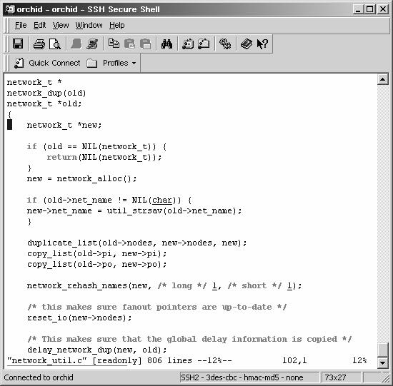
6 What is SIS? SIS is an interactive tool for synthesis and optimization of sequential and combinational circuits. Why it is so important? It serves as a framework for various algorithms can be tested and compared. It can be used standalone or integrated into other programs. It provides a well-defined library for us. The current RAMBO and GBAW are both implemented on top of the SIS library.
7 The History of SIS It was born in UC Berkeley Built on top of MIS package which is a logic optimization system in 90. The latest SIS version is sis-1.4. It is particularly useful for synthesizing and optimizing sequential circuits.
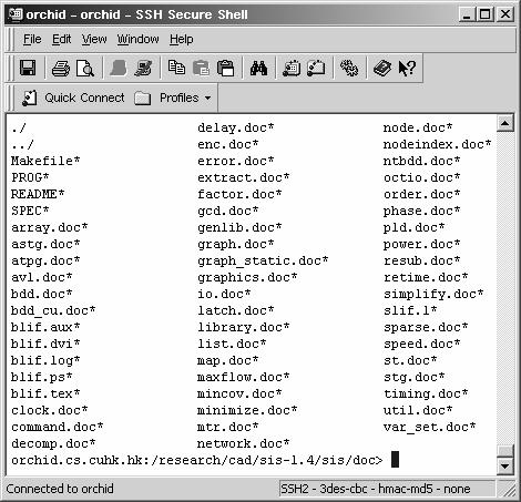
8 SIS Family It contains NOVA (State assignment) JEDI (State assignment) STAMINA (State minimization) SRED (State minimization) ESPRESSO (Boolean function minimization) BLIF2VST (BLIF to structural VHDL translator) VST2BLIF (structural VHDL to BLIF translator) XSIS (a graphical interface to SIS)

9 SIS Package
10 SIS Capabilities All the capabilities are controlled interactively by the user, include: State minimization State assignment Optimization for area and delay by using retiming Optimization by using the standard algebraic and Boolean combinational techniques from MISII,

11 SIS Shell Input your command here

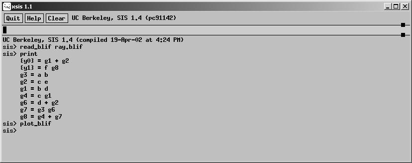
12 SIS commands?

13 Our concern SIS Library


14 SIS Library Model the circuit Model the logic gates

15 A closer look SIS library

16 Library Path
17 BLIF Format What is BLIF? Berkeley Logic Interchange Format Is it the same as our *.sis files? Yes, just different extension. It is used to describe a logic-level level hierarchical circuit in textual form. The circuit can be an arbitrary combinational or sequential network.

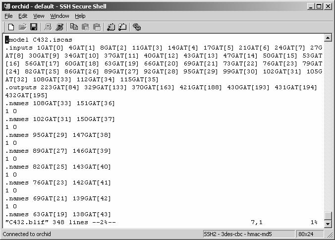
18 BLIF files

19 BLIF format Exercise : Can you sketch the circuit?
20 XSIS
21 SIS Scripts Some carefully crafted standard scripts of misii operations. Used to automate the process and guide the optimization steps. They are developed by experienced experts. Any novice designer can easily use these scripts.

22 SIS Scripts

23 Genlib Format Delay and load information Used to specify library gates in SIS. Logic function


24 How to Map Circuit? Technology mapping issue Map by mcnc1.genlib


25 How about mcnc11.genlib? Map into 2-input gates

26 Interactive Environment

27 Mapping Library

28 Script.boolean Reduce the number of literals
29 Script.algebraic
30 Area calculation A) F = X YZ X + X YZX YZ + XZ 8 literals (X,, Y, Z, X, X, Y, Z, Z, X, Z) B) F = X Y(Z X + Z ) Z ) + XZ = X Y X Y + XZ 4 literals (X,, Y, X, Z)
31 Part 2: Combinational and Sequential Circuit Synthesis
32 Outline : Circuit Synthesis Logic Synthesis Fundamentals Combinational Circuit It has outputs that depend only on the current value of the inputs. Sequential Circuit Composes of combinational logic blocks and registers. It has outputs that may depend upon the past value as well as the current input values.
33 Logic Synthesis Fundamentals Refer to CEG 5330 course materials Cover, minimum cover, prime, The Espresso Minimizer Cube, Kernel, Co-kernel Two-level logic minimization Multi-level level logic minimization Sequential vs. Combinational Technology mapping,
34 Combinational Circuit
35 Synchronous circuit & its representation
36 SDC, ODC & EDC Satisfiability don t t care sets (SDC) It captures conditions which can never happen in the network. Observability don t t care sets (ODC) It captures changes which may occur without affecting the outputs. External don t t care sets (EDC) User-specified specified
37 State Transition Graph (STG) Each state is symbolic STG and its logic representation
38 STG Manipulations From STG to netlist State minimization Produce a machine with fewer states State assignment Assign a binary code for each symbolic state A latch is used to store each bit of the binary code STG extraction Inverse of state assignment Extract the STG from the logic netlist SIS command: stg_extract
39 Sequential Circuit Optimization State minimization & assignment of FSM Retiming techniques Reduce cycle time Minimize the number of registers Cycle-Time Minimization Resynthesis Particularly use between registers Rewiring
40 Rewiring Example Both logic gates and the number of FF are reduced.
41 Part 3: Rewiring Engines
42 Outline : Rewiring Engines Introduction ATPG Technique RAMBO REWIRE RAMFIRE Graph based Technique GBAW
43 Introduction Alternative Wiring What is Alternative Wire? Add a redundant wire into a circuit (so as to make) Another wire (target( wire) ) becomes redundant Remove target wire. Without changing the circuit functionality. 2 fundamentally different approaches RAMBO/RAMFIRE Automatic Test Pattern Generation (ATPG)-based GBAW Graph-based
44 Alternative Wiring - Application 1 Useful in different areas Logic Optimization final circuit becomes smaller c g 4 b g 1 redundant d g 5 O 1 e alternative c g 2 g 6 w a wire d w r O 2 a g 7 g 8 g 9 b g 3 f target wire b g 1 d g 5 O 1 e c g 2 g 6 c a g 8 g 9 O 2 b g 3 f
45 Alternative Wiring - Application 2 Circuit Partitioning the interconnect wires between partitions is reduced from 3 to 2. e f a b O 1 e f a b O 1 c d O 2 c d O 2 (a) An alternative wire in an irredundant circuit (b) No gain for logic synthesis, but gain for partitioning
46 ATPG a b c d e f 1 0 s-a-1 1 (0/1) (0/1) Logic Circuit A Fault A Fault value A Test Vector Test Vector: (a, b, c, d, e) = (1, 0, 0, 1, 0)
47 Definition Transitive Fanin & Fanout If there is a path connected from ni to nj ni is the transitive fanin of nj nj is the transitive fanout of ni Propagation path ni nj
48 Definition Transitive Fanin & Fanout Cone Fanin Cone of wire w are the wires connecting the transitive fanins of ni Fanout Cone of wire w are the wires connecting the transitive fanouts of nj ni w nj Transitive Fanin Transitive Fanin Not Transitive
49 Definition Dominator d of a wire w All paths from w to any primary outputs have to pass through d Dominator w PO Not Dominator
50 Definition Controlling Value It determines the output value of a gate without considering the side inputs 0 for AND gate 1 for OR gate Sensitizing/non-controlling value Complement of controlling value 1 for AND gate 0 for OR gate
51 Testing Single Stuck-at (SSA) fault The wire will always give 0 or 1 Stuck-at fault Test Propagate the fault Set the dominators side inputs to sensitizing value to propagate the fault to any primary output Activate the fault Set the wire under test to 0 for s-a-1 s 1 or 1 for s-a-0s
52 Testing c 1 b d 0 g1 g4 0 g5 0 0 For Propagate Activate d->g6 stuck the fault at 1 test o1 e c d 1 a b 1 f g2 0 0 D g3 g6 D g7 1 D 0 g8 D 1 g9 D o2 Test for stuck-at 1
53 Testing The values are called Mandatory Assignment (MA) MAs must be satisfied The MAs that used to propagate the fault are called Observability Mandatory Assigment (OMA)
54 Testing c 1 b d 0 g1 g4 0 g5 0 0 Green is OMA!!! o1 e c d 1 a b 1 g2 0 0 D g3 g6 D g7 1 D 0 g8 D 1 g9 D o2 f
55 How RAMBO works c g4 b d g1 g5 o1 e c d g2 g6 g7 g8 g9 o2 a b f g3 Wire becomes redundant
56 REWIRE Proposed by Professor S.C.Chang in Fast Boolean Optimization by Rewiring in 1996 ATPG-based algorithm Speed: GBAW > REWIRE > RAMBO AWs Searching Power: RAMBO > REWIRE > GBAW
57 How REWIRE works c b d e c d g1 g2 g4 g5 g6 1. Set all the dominators side input to non-controlling value 0 2. Recursive forward implication 3. Recursive backward implication g7 g8 g9 o1 o2 Every node is a destination node, n d Find OMA for n d Generate an array of wt a b f g3 1 1
58 How REWIRE works (2) c b d e c d g1 g2 g4 g5 g6 0 g7 g8 1. Transitive fanin cone of n d 2. Transitive fanout cone of n d 3. k levels of transitive fanin of dominator of n d g9 o1 o2 Every node is a destination node, n d Find OMA for n d Generate an array of wt Filter irredundant wire from wt a b f 1 1 g wires in wt
59 How REWIRE works (3) If one of the input node of an AND {OR} gate has an OMA of 0 {1}, all other input wires are irredundant c b d e c d g1 g2 g4 g5 g6 0 g7 All the direct inputs of an AND {OR} gate are irredundant if the AND gate has an OMA of 0 {1} g8 g9 o1 o2 Every node is a destination node, n d Find OMA for n d Generate an array of wt Filter irredundant wire from wt a b f 1 1 g wires in wt
60 How REWIRE works (4) v c b d e c d a b f g1 g2 0 g3 0 D_ 1 g4 g5 g6 0 0 D_ g7 D_ 1 g8 D_ Suppose we consider d->g6 g9 D_ o1 o2 Every node is a destination node, n d Find OMA for n d Generate an array of wt Filter irredundant wire from wt Perform stuck-at-fault test at wt Determination of alternative wires Finally, we get the alternative wire g1->g6 and o1->g6 for target wire d->g6
61 RAMFIRE - Single-Pass Redundancy Addition And Removal Operation 1: Given a target wire w t to be removed, which redundant wires, when added, will make w t redundant? Operation 2: After the addition of a redundant wire w a, which wires become redundant and hence removable? RAMFIRE identifies redundant wires in one pass without trial-and and-error search.
62 GBAW * -- No Need of Boolean Knowledge. High Locality properties on AWs observed in benchmarks (analogy: RISC v.s. CISC) Topological locality: 96% 1 st. Aws are 2-local2 Pattern locality: very uneven appearance of AWs patterns Application locality: probably no need to try all patterns A Pre-analyzed Pattern (graph) - based AW Scheme Methodology: pattern matching Advantage: Fast, As Effective No need for porting ATPG package Equally easy to do backward transformations *received Honorable Mention Award of IEEE International VLSI Design 2000
63 GBAW Most AWs are close to target wires Graph-based AW scheme Search alternative wire by isomorphism between local sub-networks and the pre-defined patterns. Easy for both forward and backward search. Use Configuration to denote a Boolean network. No need of Boolean implication/operations. Powerful in finding alternative wires and Very Fast!
64 GBAW Configuration A Boolean network G with its sub-network S. Below shows the mapping from network to configuration. Node y define as a triplet (op, d - (y), d + (y)) op is the Boolean operator (AND, OR, NAND, NOR) d - (y)) is the in-degree of y, d + (y)) is the out-degree of y. (AND, dc, dc) both fanins or fanouts are also don t t care. a b g 1 S g 2 g 3 G f 1 c d f 2 (a) Boolean network G (AND,2,1) (AND,2,2) (AND,dc,1) (AND,dc,dc) a g 1 g 2 a g 1 g 2 b c b c D 1 D 2 (b) A configuration of S (c) Another configuration of S
65 How GBAW works Pattern Matching No Boolean implication a g1 g2 2-Local Pattern b g3 g4 g7 g8 c g6 g5
66 0-local pattern Bold line target wire Dotted line alternative wire 0-local means the edge distance between target and alternative wire is 0. (op 1,k,dc) (dc,dc,dc) a 1 a 2 g 1 g 2 a k g 3 (op 3,k,dc) g 4 (dc,dc,dc)
67 1-local patterns AND AND (or NAND) a (op 1,dc,1) g 1 (op 2,dc,dc) g 2 (a) Case 1-1, op 1 =AND, op 2 =AND (or NAND); or op 1 =OR, op 2 =OR(or NOR) (op 1,k,dc) a 1 g 1 a 2... a k (op 2,k,dc) g 2 (b) Case 1-2, op 1 =AND, op 2 =AND (or NAND); or op 1 =OR, op 2 =OR(or NOR) AND AND (or NAND) a (op 1,dc,1) g 1 (op 2,dc,dc) g 2 (c) Case 1-3, op 1 =NOR, op 2 =NAND (or AND); or op 1 =NAND, op 2 =OR(or NOR)
68 2-local patterns (NOR,dc,1) (NAND,dc,1) (NOR,dc,dc) a g 1 g 2 g 3 (OR,dc,1) (a) Case 2-1 (AND,dc,1) a 1 a 2... a k g 1 g 4 g 2 g 2 (NOR,dc,dc) or (OR,dc,dc) Forward alternative wire Backward alternative wire (AND,k,dc) (b) Case 2-2 dc (OR,dc,h) (AND,t,1) (OR,dc,dc) 1... t-1 dc (OR,s,dc) (AND,h,dc) dc 1... s-1 dc dc (c) Case 2-3 (AND,s,dc)
69 Forward & Backward capabilities Implement Reverse Searching Increase GBAW s search power Forward Order Search from fanin to fanout Search from fanout to fanin Backward Order
70 Verification of 2-local 2 pattern x (a*x) y ((a*x) *y) z (((a*x) *y) *z) Target wire exists: g 3 = (((a*x) *y)*z) *y)*z) = (((a +x +x )*y)*z) )*y)*z) = ((a y + x y)*z) )*z) Alternative wire exists: g 3 = ((a y) *( *(x y) *z) = original g 3
71 Pattern Clusters a What is the meaning of pattern Clusters? g3 2-Local Pattern (Cluster 3 Set 6a) a g1 g2 g3 b1 g5 b2 b g4 2-Local Pattern (Cluster 1) bn
72 Pattern Locality Matching Found Pattern Name Matching Found _2a 2_3a 2_4a 2_5 2_n3_2 2_n3_4 2_n3_6 Very uneven appearance of AW patterns Top figure: Pattern Locality for 1-1 Local Bottom figure: Pattern Locality for 2-2 Local Pattern Name

73 Rewiring GUI interface Benchmark: small.blif The current user interface allows users interactively locate any possible redundant rewires in the circuit by using either GBAW, RAMBO and REWIRE.

74 Rewiring GUI interface Benchmark: des.blif The system is built on top of Java and C languages.
75 Rewiring Framework application? application 3 Area 2 5? Power 4? 1 Delay efficient rewire engine design methodology RAMBO / GBAW / Logical/Physical Co-Design Applicationindependent rewiring engine provides efficient routines for for logic logic alternative exploration
76 Part 4 Implementation details Checking fan-in and fan-out and lab exercises Using sr_local2_n3_6.c as an example, we show how the code run and how the node is named
77 main() [program initialization] sram(); [statistic reporting] [statistic reporting]
78 sram() for a wire <node1< -> fanout1> transformxxx xxx(wire); [match different AW patterns]
79 For greedy simplification sram() for a wire <node1< -> fanout1> transformxxx xxx(wire); [match different AW patterns] [transform the first matched pattern]
80 For incremental perturbation sram() for a wire <node1< -> fanout1> transformxxx xxx(wire); [match different AW patterns] [record all matched patterns] transform_incremental(); [transform the min-cost pattern]
81 Check if any element with the structure is NULL (Function is_node_ok is defined in sr_util.c) /*** fanout1 ***/ if (!is_node_ok(fanout1)) if (gate_type(fanout1)!= T_NOT) fo1_not = fanout1; fanout1 = node_get_fanout(fo1_not, 0); node1 Not Not yet yet checked checked Checking Checking Require Require further further checking checking Checked Checked fanout1 a g 1 g 2 g 3 g 5 b g 4 if (!is_node_ok(fanout1)) if (gate_type(fanout1) == T_PO) if (node_num_fanin(fanout1)!= 2) if (node_num_fanout(fanout1)!= 1) /*** fanout2 ***/ fanout2 = node_get_fanout(fanout1, 0); if (!is_node_ok(fanout2)) if (gate_type(fanout2) == T_PO) if (node_num_fanout(fanout2)!= 1) if (node_num_fanin(fanout2)!= 2) /*** fanout3 ***/ fanout3 = node_get_fanout(fanout2, 0); if (!is_node_ok(fanout3)) if (gate_type(fanout3) == T_PO)
82 Check whether the fan-out of fanout1 is a NOT gate /*** fanout1 ***/ if (!is_node_ok(fanout1)) if (gate_type(fanout1)!= T_NOT) fo1_not = fanout1; fanout1 = node_get_fanout(fo1_not, 0); if (!is_node_ok(fanout1)) if (gate_type(fanout1) == T_PO) if (node_num_fanin(fanout1)!= 2) if (node_num_fanout(fanout1)!= 1) node1 fanout1 a g 1 g 2 g 3 g 5 b g 4 /*** fanout2 ***/ fanout2 = node_get_fanout(fanout1, 0); if (!is_node_ok(fanout2)) if (gate_type(fanout2) == T_PO) if (node_num_fanout(fanout2)!= 1) if (node_num_fanin(fanout2)!= 2) /*** fanout3 ***/ fanout3 = node_get_fanout(fanout2, 0); if (!is_node_ok(fanout3)) if (gate_type(fanout3) == T_PO)
83 /*** fanout1 ***/ if (!is_node_ok(fanout1)) Rename fanout1 to fo1_not if (gate_type(fanout1)!= T_NOT) fanout1 now become the fan-out of the NOT gate fo1_not = fanout1; fanout1 = node_get_fanout(fo1_not, 0); if (!is_node_ok(fanout1)) if (gate_type(fanout1) == T_PO) if (node_num_fanin(fanout1)!= 2) if (node_num_fanout(fanout1)!= 1) node1 fo1_not fanout1 a g 1 g 2 g 3 g 5 b g 4 /*** fanout2 ***/ fanout2 = node_get_fanout(fanout1, 0); if (!is_node_ok(fanout2)) if (gate_type(fanout2) == T_PO) if (node_num_fanout(fanout2)!= 1) if (node_num_fanin(fanout2)!= 2) /*** fanout3 ***/ fanout3 = node_get_fanout(fanout2, 0); if (!is_node_ok(fanout3)) if (gate_type(fanout3) == T_PO)
84 Again check if any element with the structure is NULL /*** fanout1 ***/ if (!is_node_ok(fanout1)) if (gate_type(fanout1)!= T_NOT) fo1_not = fanout1; fanout1 = node_get_fanout(fo1_not, 0); if (!is_node_ok(fanout1)) if (gate_type(fanout1) == T_PO) if (node_num_fanin(fanout1)!= 2) if (node_num_fanout(fanout1)!= 1) node1 fo1_not fanout1 a g 1 g 2 g 3 g 5 b g 4 /*** fanout2 ***/ fanout2 = node_get_fanout(fanout1, 0); if (!is_node_ok(fanout2)) if (gate_type(fanout2) == T_PO) if (node_num_fanout(fanout2)!= 1) if (node_num_fanin(fanout2)!= 2) /*** fanout3 ***/ fanout3 = node_get_fanout(fanout2, 0); if (!is_node_ok(fanout3)) if (gate_type(fanout3) == T_PO)
85 Fan-out of fanout cannot be Primary Output /*** fanout1 ***/ if (!is_node_ok(fanout1)) if (gate_type(fanout1)!= T_NOT) fo1_not = fanout1; fanout1 = node_get_fanout(fo1_not, 0); if (!is_node_ok(fanout1)) if (gate_type(fanout1) == T_PO) if (node_num_fanin(fanout1)!= 2) if (node_num_fanout(fanout1)!= 1) node1 fo1_not fanout1 a g 1 g 2 g 3 g 5 b g 4 /*** fanout2 ***/ fanout2 = node_get_fanout(fanout1, 0); if (!is_node_ok(fanout2)) if (gate_type(fanout2) == T_PO) if (node_num_fanout(fanout2)!= 1) if (node_num_fanin(fanout2)!= 2) /*** fanout3 ***/ fanout3 = node_get_fanout(fanout2, 0); if (!is_node_ok(fanout3)) if (gate_type(fanout3) == T_PO)
86 fanout1 must have 2 fan-in(s) /*** fanout1 ***/ if (!is_node_ok(fanout1)) if (gate_type(fanout1)!= T_NOT) fo1_not = fanout1; fanout1 = node_get_fanout(fo1_not, 0); if (!is_node_ok(fanout1)) if (gate_type(fanout1) == T_PO) if (node_num_fanin(fanout1)!= 2) if (node_num_fanout(fanout1)!= 1) node1 fo1_not fanout1 a g 1 g 2 g 3 g 5 b g 4 /*** fanout2 ***/ fanout2 = node_get_fanout(fanout1, 0); if (!is_node_ok(fanout2)) if (gate_type(fanout2) == T_PO) if (node_num_fanout(fanout2)!= 1) if (node_num_fanin(fanout2)!= 2) /*** fanout3 ***/ fanout3 = node_get_fanout(fanout2, 0); if (!is_node_ok(fanout3)) if (gate_type(fanout3) == T_PO)
87 fanout1 must have 1 fan-out /*** fanout1 ***/ if (!is_node_ok(fanout1)) if (gate_type(fanout1)!= T_NOT) fo1_not = fanout1; fanout1 = node_get_fanout(fo1_not, 0); if (!is_node_ok(fanout1)) if (gate_type(fanout1) == T_PO) if (node_num_fanin(fanout1)!= 2) if (node_num_fanout(fanout1)!= 1) node1 fo1_not fanout1 a g 1 g 2 g 3 g 5 b g 4 /*** fanout2 ***/ fanout2 = node_get_fanout(fanout1, 0); if (!is_node_ok(fanout2)) if (gate_type(fanout2) == T_PO) if (node_num_fanout(fanout2)!= 1) if (node_num_fanin(fanout2)!= 2) /*** fanout3 ***/ fanout3 = node_get_fanout(fanout2, 0); if (!is_node_ok(fanout3)) if (gate_type(fanout3) == T_PO)
88 Name fanout2 be the fan-out of fanout1 /*** fanout1 ***/ if (!is_node_ok(fanout1)) if (gate_type(fanout1)!= T_NOT) fo1_not = fanout1; fanout1 = node_get_fanout(fo1_not, 0); if (!is_node_ok(fanout1)) if (gate_type(fanout1) == T_PO) if (node_num_fanin(fanout1)!= 2) if (node_num_fanout(fanout1)!= 1) node1 fanout1 fanout2 fo1_not a g 1 g 2 g 3 g 5 b g 4 /*** fanout2 ***/ fanout2 = node_get_fanout(fanout1, 0); if (!is_node_ok(fanout2)) if (gate_type(fanout2) == T_PO) if (node_num_fanout(fanout2)!= 1) if (node_num_fanin(fanout2)!= 2) /*** fanout3 ***/ fanout3 = node_get_fanout(fanout2, 0); if (!is_node_ok(fanout3)) if (gate_type(fanout3) == T_PO)
89 Check if any element with the structure is NULL /*** fanout1 ***/ if (!is_node_ok(fanout1)) if (gate_type(fanout1)!= T_NOT) fo1_not = fanout1; fanout1 = node_get_fanout(fo1_not, 0); if (!is_node_ok(fanout1)) if (gate_type(fanout1) == T_PO) if (node_num_fanin(fanout1)!= 2) if (node_num_fanout(fanout1)!= 1) node1 fanout1 fanout2 fo1_not a g 1 g 2 g 3 g 5 b g 4 /*** fanout2 ***/ fanout2 = node_get_fanout(fanout1, 0); if (!is_node_ok(fanout2)) if (gate_type(fanout2) == T_PO) if (node_num_fanout(fanout2)!= 1) if (node_num_fanin(fanout2)!= 2) /*** fanout3 ***/ fanout3 = node_get_fanout(fanout2, 0); if (!is_node_ok(fanout3)) if (gate_type(fanout3) == T_PO)
90 Fan-out of fanout2 cannot be Primary Output /*** fanout1 ***/ if (!is_node_ok(fanout1)) if (gate_type(fanout1)!= T_NOT) fo1_not = fanout1; fanout1 = node_get_fanout(fo1_not, 0); if (!is_node_ok(fanout1)) if (gate_type(fanout1) == T_PO) if (node_num_fanin(fanout1)!= 2) if (node_num_fanout(fanout1)!= 1) node1 fanout1 fanout2 fo1_not a g 1 g 2 g 3 g 5 b g 4 /*** fanout2 ***/ fanout2 = node_get_fanout(fanout1, 0); if (!is_node_ok(fanout2)) if (gate_type(fanout2) == T_PO) if (node_num_fanout(fanout2)!= 1) if (node_num_fanin(fanout2)!= 2) /*** fanout3 ***/ fanout3 = node_get_fanout(fanout2, 0); if (!is_node_ok(fanout3)) if (gate_type(fanout3) == T_PO)
91 Number of fan-out of fanout2 must be 1 /*** fanout1 ***/ if (!is_node_ok(fanout1)) if (gate_type(fanout1)!= T_NOT) fo1_not = fanout1; fanout1 = node_get_fanout(fo1_not, 0); if (!is_node_ok(fanout1)) if (gate_type(fanout1) == T_PO) if (node_num_fanin(fanout1)!= 2) if (node_num_fanout(fanout1)!= 1) node1 fanout1 fanout2 fo1_not a g 1 g 2 g 3 g 5 b g 4 /*** fanout2 ***/ fanout2 = node_get_fanout(fanout1, 0); if (!is_node_ok(fanout2)) if (gate_type(fanout2) == T_PO) if (node_num_fanout(fanout2)!= 1) if (node_num_fanin(fanout2)!= 2) /*** fanout3 ***/ fanout3 = node_get_fanout(fanout2, 0); if (!is_node_ok(fanout3)) if (gate_type(fanout3) == T_PO)
92 Number of fan-in(s) of fanout2 must be 2 /*** fanout1 ***/ if (!is_node_ok(fanout1)) if (gate_type(fanout1)!= T_NOT) fo1_not = fanout1; fanout1 = node_get_fanout(fo1_not, 0); if (!is_node_ok(fanout1)) if (gate_type(fanout1) == T_PO) if (node_num_fanin(fanout1)!= 2) if (node_num_fanout(fanout1)!= 1) node1 fanout1 fanout2 fo1_not a g 1 g 2 g 3 g 5 b g 4 /*** fanout2 ***/ fanout2 = node_get_fanout(fanout1, 0); if (!is_node_ok(fanout2)) if (gate_type(fanout2) == T_PO) if (node_num_fanout(fanout2)!= 1) if (node_num_fanin(fanout2)!= 2) /*** fanout3 ***/ fanout3 = node_get_fanout(fanout2, 0); if (!is_node_ok(fanout3)) if (gate_type(fanout3) == T_PO)
93 Name fan-out of fanout2 be fanout3 /*** fanout1 ***/ if (!is_node_ok(fanout1)) if (gate_type(fanout1)!= T_NOT) node1 fanout1 fanout2 fanout3 fo1_not a g 1 g 2 g 3 g 5 b g 4 fo1_not = fanout1; fanout1 = node_get_fanout(fo1_not, 0); if (!is_node_ok(fanout1)) if (gate_type(fanout1) == T_PO) if (node_num_fanin(fanout1)!= 2) if (node_num_fanout(fanout1)!= 1) /*** fanout2 ***/ fanout2 = node_get_fanout(fanout1, 0); if (!is_node_ok(fanout2)) if (gate_type(fanout2) == T_PO) if (node_num_fanout(fanout2)!= 1) if (node_num_fanin(fanout2)!= 2) /*** fanout3 ***/ fanout3 = node_get_fanout(fanout2, 0); if (!is_node_ok(fanout3)) if (gate_type(fanout3) == T_PO)
94 Check if any element with the structure is NULL node1 fanout1 fanout2 fanout3 fo1_not a g 1 g 2 g 3 g 5 b g 4 /*** fanout1 ***/ if (!is_node_ok(fanout1)) if (gate_type(fanout1)!= T_NOT) fo1_not = fanout1; fanout1 = node_get_fanout(fo1_not, 0); if (!is_node_ok(fanout1)) if (gate_type(fanout1) == T_PO) if (node_num_fanin(fanout1)!= 2) if (node_num_fanout(fanout1)!= 1) /*** fanout2 ***/ fanout2 = node_get_fanout(fanout1, 0); if (!is_node_ok(fanout2)) if (gate_type(fanout2) == T_PO) if (node_num_fanout(fanout2)!= 1) if (node_num_fanin(fanout2)!= 2) /*** fanout3 ***/ fanout3 = node_get_fanout(fanout2, 0); if (!is_node_ok(fanout3)) if (gate_type(fanout3) == T_PO)
95 fanout3 itself cannot be Primary Output /*** fanout1 ***/ if (!is_node_ok(fanout1)) if (gate_type(fanout1)!= T_NOT) node1 fanout1 fanout2 fanout3 fo1_not a g 1 g 2 g 3 g 5 b g 4 fo1_not = fanout1; fanout1 = node_get_fanout(fo1_not, 0); if (!is_node_ok(fanout1)) if (gate_type(fanout1) == T_PO) if (node_num_fanin(fanout1)!= 2) if (node_num_fanout(fanout1)!= 1) /*** fanout2 ***/ fanout2 = node_get_fanout(fanout1, 0); if (!is_node_ok(fanout2)) if (gate_type(fanout2) == T_PO) if (node_num_fanout(fanout2)!= 1) if (node_num_fanin(fanout2)!= 2) /*** fanout3 ***/ fanout3 = node_get_fanout(fanout2, 0); if (!is_node_ok(fanout3)) if (gate_type(fanout3) == T_PO)
96 gt_fo1 = gate_type(fanout1); gt_fo2 = gate_type(fanout2); gt_fo3 = gate_type(fanout3); Now, let s consider this block of codes Name the other fan-in of fanout2 be fanin1 Check if fanin1 a non-primary output and has only 1 fan-out node1 fanout1 fanout2 fanout3 fo1_not a g 1 g 2 g 3 g 5 fanin1 b g 4 /*** fanin1 ***/ match=0; foreach_fanin(fanout2,j1,temp){ if (temp == fanout1) continue; fanin1 = temp; if (!is_node_ok(fanin1)) continue; if (gate_type(fanin1) == T_PO) continue; if (node_num_fanout(fanin1)!= 1) continue; gt_fi1 = gate_type(fanin1); foreach_fanin(fanin1,j2,temp){ fanin2 = temp; if (!is_node_ok(fanin2)) continue; if (gate_type(fanin2) == T_PO) continue; if (gate_type(fanin2)!= T_NOT) continue; node2 = node_get_fanin(fanin2, 0); if (!is_node_ok(node2)) continue; if (gate_type(node2) == T_PO) continue; foreach_fanin(fanout1,j3,temp){ fanin3 = temp; if (!is_node_ok(fanin3)) continue; if (gate_type(fanin3) == T_PO) continue; if (!strcmp(fanin3->name, node1->name)) continue; if (!strcmp(fanin3->name, node2->name)){ match=1; break; } if (match==1) break; } if (match==1) break; } if (match==1) break; } if (match==0)
97 gt_fo1 = gate_type(fanout1); gt_fo2 = gate_type(fanout2); gt_fo3 = gate_type(fanout3); Here are 3 nested for-loop (Marco) Name the fan-in of fanin1 to fanin2 fanin2 must be a NOT gate and must be be a Primary Output Name the fan-in of fanin2 to node2 match is a flag that check whether node2 is also fan-in of fanout1 node1 fanout1 fanout2 fanout3 fo1_not a g 1 g 2 g 3 fanin2 g 5 fanin1 b g node2 4 /*** fanin1 ***/ match=0; foreach_fanin(fanout2,j1,temp){ if (temp == fanout1) continue; fanin1 = temp; if (!is_node_ok(fanin1)) continue; if (gate_type(fanin1) == T_PO) continue; if (node_num_fanout(fanin1)!= 1) continue; gt_fi1 = gate_type(fanin1); foreach_fanin(fanin1,j2,temp){ fanin2 = temp; if (!is_node_ok(fanin2)) continue; if (gate_type(fanin2) == T_PO) continue; if (gate_type(fanin2)!= T_NOT) continue; node2 = node_get_fanin(fanin2, 0); if (!is_node_ok(node2)) continue; if (gate_type(node2) == T_PO) continue; foreach_fanin(fanout1,j3,temp){ fanin3 = temp; if (!is_node_ok(fanin3)) continue; if (gate_type(fanin3) == T_PO) continue; if (!strcmp(fanin3->name, node1->name)) continue; if (!strcmp(fanin3->name, node2->name)){ match=1; break; } if (match==1) break; } if (match==1) break; } if (match==1) break; } if (match==0)
98 Here are also several nested for-loop After performing some checking, we determine whether both node1 and node2 eventually meet at g4 after passing through a NOT gate. Finally, we check whether the combination of logic gates match the possible patterns node1 fanout1 fanout2 fanout3 fo1_not a g 1 g 2 g 3 /*** g4 ***/ /*** cluster a ***/ match=0; foreach_fanout(node1, gen1, fanout11) { if (!is_node_ok(fanout11)) continue; if (gate_type(fanout11) == T_PO) continue; if (!strcmp(fo1_not->name, fanout11->name)) continue; if (node_num_fanin(fanout11)!= 2) continue; foreach_fanout(node2, gen3, fanout12) { if (!is_node_ok(fanout12)) continue; if (gate_type(fanout12) == T_PO) continue; if (node_num_fanin(fanout12)!= 2) continue; if (!strcmp(fanout1->name, fanout12->name)) continue; if (!strcmp(fanout11->name, fanout12->name)){ if (((gt_fo3 == T_NAND) (gt_fo3 == T_AND))&& ( ((gt_fi1 == T_OR)&&(gt_fo2 == T_NAND)&&(gt_fo1 == T_OR)) ((gt_fi1 == T_NOR)&&(gt_fo2 == T_OR)&&(gt_fo1 == T_NOR)) )){ if (gate_type(fanout12) == T_OR){ not = 0; match=1; break; } else if (gate_type(fanout12) == T_NOR){ not = 1; match=1; break; } } else if (((gt_fo3 == T_NOR) (gt_fo3 == T_OR))&& ( ((gt_fi1 == T_OR)&&(gt_fo2 == T_AND)&&(gt_fo1 == T_OR)) ((gt_fi1 == T_NOR)&&(gt_fo2 == T_NOR)&&(gt_fo1 == T_NOR)) )){ if (gate_type(fanout12) == T_NOR){ not = 0; match=1; break; } else if (gate_type(fanout12) == T_OR){ not = 1; match=1; break; } } else if (((gt_fo3 == T_NAND) (gt_fo3 == T_AND))&&( ((gt_fi1 == T_AND)&&(gt_fo2 == T_OR)&&(gt_fo1 == T_AND)) ((gt_fi1 == T_NAND)&&(gt_fo2 == T_NAND)&&(gt_fo1 == T_NAND)) )){ if (gate_type(fanout12) == T_NAND){ not = 0; match=1; break; } else if (gate_type(fanout12) == T_AND){ not = 1; match=1; break; b node2 fanin2 g 5 fanin1 g 4 } } else if (((gt_fo3 == T_NOR) (gt_fo3 == T_OR))&&( ((gt_fi1 == T_AND)&&(gt_fo2 == T_NOR)&&(gt_fo1 == T_AND)) ((gt_fi1 == T_NAND)&&(gt_fo2 == T_AND)&&(gt_fo1 == T_NAND)) )){ if (gate_type(fanout12) == T_AND){ not = 0; match=1; break; } else if (gate_type(fanout12) == T_NAND){ not = 1; match=1; break; } } } if (match==1) break; } if (match==1) break; }
99 #ifdef WIRE printf("2_n3_6 add: %s to %s\n",fanout11->name, fanout3->name); printf("2_n3_6 rm: %s to %s\n",fo1_not->name, fanout1->name); printf("2_n3_6 rm: %s to %s\n",fanin2->name, fanin1->name); #endif #ifdef TRANSFORM_ALL_AW if (not == 0) do_add(fanout11,fanout3,t_buf,0); else if (not == 1) do_add(fanout11,fanout3,t_not,0); do_rm(fo1_not,fanout1); do_rm(fanin2,fanin1); #endif #ifdef LOGIC_OPTIMIZATION add_aw(node1, fanout1, node1, fanout2, T_BUF,0,12301); #endif return MY_OK; node1 fanout1 fanout2 fanout3 fo1_not If the 2_n3_6 pattern is found, the result will be display in stdout, perform redundancy addition and removal and logic optimization a g 1 g 2 g 3 g 5 fanin1 b node2 fanin2 g 4

100 Warm-up exercise
101 Answer of warming up exercise Finding the occurrence of pattern 2_n3_6 in circuit C7552.sis
102 How to get the answer Consider the code segment in sr_main.c #ifdef NEW_CLUSTER_3 #ifdef WIRE #endif flag1 = transform2_n3_6(node1, fanout1); if (flag1 == MY_OK) { printf("local 2_n3_6: Node %s -> Node %s.\n", node1_name,fanout1_name); After pattern is found, Local 2_n3_6 will be printed to stdout./gbaw.test /test/c7552.sis grep Local 2_n3_6 Number of lines give the number of pattern found
103 How to get the answer (con( con t) Output Local 2_n3_6: Node [60016] -> Node [61726]. Local 2_n3_6: Node [60292] -> Node [61970]. Local 2_n3_6: Node [60294] -> Node [62480]. Local 2_n3_6: Node [60317] -> Node [62350]. Local 2_n3_6: Node [60319] -> Node [62397]. Local 2_n3_6: Node [60321] -> Node [62289]. Local 2_n3_6: Node [60323] -> Node [62408]. Local 2_n3_6: Node [60365] -> Node [61983]. Local 2_n3_6: Node [60367] -> Node [62433]. Local 2_n3_6: Node [60339] -> Node [62241]. Local 2_n3_6: Node [60341] -> Node [62523]. Local 2_n3_6: Node [60274] -> Node [61806]. Local 2_n3_6: Node [60276] -> Node [61885]. Local 2_n3_6: Node [60270] -> Node [61796]. Local 2_n3_6: Node [60272] -> Node [61859]. Local 2_n3_6: Node [60230] -> Node [61850]. Local 2_n3_6: Node [60226] -> Node [61839]. Local 2_n3_6: Node [60228] -> Node [62027]. Totally 18 pattern is matched
104 Topological Statistics Exercise To change the Distribution Locality Version into Topological Locality Version & obtain statistics for both versions on circuits starts with C, e.g. C3540.sis, etc Verification of Stat can be found in ICCAD_02.doc document.

105 File hierarchy Source code Technical papers FYP Reports FYP Presentations Today s s slides GBAW statistics Today s s benchmark
106 Thanks for your patience!
SIS: A System for Sequential Circuit Synthesis
 SIS: A System for Sequential Circuit Synthesis Electronics Research Laboratory Memorandum No. UCB/ERL M92/41 Ellen M. Sentovich Kanwar Jit Singh Luciano Lavagno Cho Moon Rajeev Murgai Alexander Saldanha
SIS Logic Synthesis System
 SIS Logic Synthesis System Michele Lora Tiziano Villa University of Verona Dep. Computer Science Italy Slides courtesy of Giuseppe and Luigi Di Guglielmo, Davide Bresolin, Michele Lora and Tiziano Villa
CSE241 VLSI Digital Circuits UC San Diego
 CSE241 VLSI Digital Circuits UC San Diego Winter 2003 Lecture 05: Logic Synthesis Cho Moon Cadence Design Systems January 21, 2003 CSE241 L5 Synthesis.1 Kahng & Cichy, UCSD 2003 Outline Introduction Two-level
VLSI System Design Part II : Logic Synthesis (1) Oct Feb.2007
 Oct Feb.2007") VLSI System Design Part II : Logic Synthesis (1) Oct.2006 - Feb.2007 Lecturer : Tsuyoshi Isshiki Dept. Communications and Integrated Systems, Tokyo Institute of Technology isshiki@vlsi.ss.titech.ac.jp
VLSI System Design Part II : Logic Synthesis (1) Oct.2006 - Feb.2007 Lecturer : Tsuyoshi Isshiki Dept. Communications and Integrated Systems, Tokyo Institute of Technology isshiki@vlsi.ss.titech.ac.jp
Functional extension of structural logic optimization techniques
 Functional extension of structural logic optimization techniques J. A. Espejo, L. Entrena, E. San Millán, E. Olías Universidad Carlos III de Madrid # e-mail: { ppespejo, entrena, quique, olias}@ing.uc3m.es
ECE260B CSE241A Winter Logic Synthesis
 ECE260B CSE241A Winter 2007 Logic Synthesis Website: /courses/ece260b-w07 ECE 260B CSE 241A Static Timing Analysis 1 Slides courtesy of Dr. Cho Moon Introduction Why logic synthesis? Ubiquitous used almost
1/28/2013. Synthesis. The Y-diagram Revisited. Structural Behavioral. More abstract designs Physical. CAD for VLSI 2
 Synthesis The Y-diagram Revisited Structural Behavioral More abstract designs Physical CAD for VLSI 2 1 Structural Synthesis Behavioral Physical CAD for VLSI 3 Structural Processor Memory Bus Behavioral
Don't Cares in Multi-Level Network Optimization. Hamid Savoj. Abstract
 Don't Cares in Multi-Level Network Optimization Hamid Savoj University of California Berkeley, California Department of Electrical Engineering and Computer Sciences Abstract An important factor in the
Reference. Wayne Wolf, FPGA-Based System Design Pearson Education, N Krishna Prakash,, Amrita School of Engineering
 FPGA Fabrics Reference Wayne Wolf, FPGA-Based System Design Pearson Education, 2004 Logic Design Process Combinational logic networks Functionality. Other requirements: Size. Power. Primary inputs Performance.
Chapter 3. Gate-Level Minimization. Outlines
 Chapter 3 Gate-Level Minimization Introduction The Map Method Four-Variable Map Five-Variable Map Outlines Product of Sums Simplification Don t-care Conditions NAND and NOR Implementation Other Two-Level
Outline. EECS Components and Design Techniques for Digital Systems. Lec 11 Putting it all together Where are we now?
 Outline EECS 5 - Components and Design Techniques for Digital Systems Lec Putting it all together -5-4 David Culler Electrical Engineering and Computer Sciences University of California Berkeley Top-to-bottom
VLSI Test Technology and Reliability (ET4076)
") VLSI Test Technology and Reliability (ET476) Lecture 5 Combinational Circuit Test Generation (Chapter 7) Said Hamdioui Computer Engineering Lab elft University of Technology 29-2 Learning aims of today
VLSI Test Technology and Reliability (ET476) Lecture 5 Combinational Circuit Test Generation (Chapter 7) Said Hamdioui Computer Engineering Lab elft University of Technology 29-2 Learning aims of today
Unit 4: Formal Verification
 Course contents Unit 4: Formal Verification Logic synthesis basics Binary-decision diagram (BDD) Verification Logic optimization Technology mapping Readings Chapter 11 Unit 4 1 Logic Synthesis & Verification
ELCT201: DIGITAL LOGIC DESIGN
 ELCT201: DIGITAL LOGIC DESIGN Dr. Eng. Haitham Omran, haitham.omran@guc.edu.eg Dr. Eng. Wassim Alexan, wassim.joseph@guc.edu.eg Lecture 3 Following the slides of Dr. Ahmed H. Madian محرم 1439 ه Winter
CS8803: Advanced Digital Design for Embedded Hardware
 CS883: Advanced Digital Design for Embedded Hardware Lecture 2: Boolean Algebra, Gate Network, and Combinational Blocks Instructor: Sung Kyu Lim (limsk@ece.gatech.edu) Website: http://users.ece.gatech.edu/limsk/course/cs883
Overview. Design flow. Principles of logic synthesis. Logic Synthesis with the common tools. Conclusions
 Logic Synthesis Overview Design flow Principles of logic synthesis Logic Synthesis with the common tools Conclusions 2 System Design Flow Electronic System Level (ESL) flow System C TLM, Verification,
Sequential Logic Synthesis
 Sequential Logic Synthesis Logic Circuits Design Seminars WS2010/2011, Lecture 9 Ing. Petr Fišer, Ph.D. Department of Digital Design Faculty of Information Technology Czech Technical University in Prague
VLSI System Testing. Outline
 ECE 538 VLSI System Testing Krish Chakrabarty Test Generation: 2 ECE 538 Krish Chakrabarty Outline Problem with -Algorithm POEM FAN Fault-independent ATPG Critical path tracing Random test generation Redundancy
ESE535: Electronic Design Automation. Today. LUT Mapping. Simplifying Structure. Preclass: Cover in 4-LUT? Preclass: Cover in 4-LUT?
 ESE55: Electronic Design Automation Day 7: February, 0 Clustering (LUT Mapping, Delay) Today How do we map to LUTs What happens when IO dominates Delay dominates Lessons for non-luts for delay-oriented
SIS Logic Synthesis System
 SIS Logic Synthesis System Luigi Di Guglielmo Davide Bresolin Tiziano Villa University of Verona Dep. Computer Science Italy Introduc>on Logic Synthesis performs the transla>on from a high level descrip>on
ELCT201: DIGITAL LOGIC DESIGN
 ELCT201: DIGITAL LOGIC DESIGN Dr. Eng. Haitham Omran, haitham.omran@guc.edu.eg Dr. Eng. Wassim Alexan, wassim.joseph@guc.edu.eg Lecture 3 Following the slides of Dr. Ahmed H. Madian ذو الحجة 1438 ه Winter
Variable, Complement, and Literal are terms used in Boolean Algebra.
 We have met gate logic and combination of gates. Another way of representing gate logic is through Boolean algebra, a way of algebraically representing logic gates. You should have already covered the
Chapter 8. 8 Minimization Techniques. 8.1 Introduction. 8.2 Single-Output Minimization Design Constraints
 8 Minimization Techniques 8.1 Introduction The emphasis is on clean, irredundant, minimal designs has been dramatically affected by the evolution of LSI [VLSI] technology. There are instances where a minimal
COE 561 Digital System Design & Synthesis Introduction
 1 COE 561 Digital System Design & Synthesis Introduction Dr. Aiman H. El-Maleh Computer Engineering Department King Fahd University of Petroleum & Minerals Outline Course Topics Microelectronics Design
Redundant States in Sequential Circuits
 Redundant States in Sequential Circuits Removal of redundant states is important because Cost: the number of memory elements is directly related to the number of states Complexity: the more states the
ECE260B CSE241A Winter Logic Synthesis
 ECE260B CSE241A Winter 2005 Logic Synthesis Website: / courses/ ece260bw05 ECE 260B CSE 241A Static Timing Analysis 1 Slides courtesy of Dr. Cho Moon Introduction Why logic synthesis? Ubiquitous used almost
MVSIS v1.1 Manual. Jie-Hong Jiang, Yunjian Jiang, Yinghua Li, Alan Mishchenko*, Subarna Sinha Tiziano Villa**, Robert Brayton
 MVSIS v1.1 Manual Jie-Hong Jiang, Yunjian Jiang, Yinghua Li, Alan Mishchenko*, Subarna Sinha Tiziano Villa**, Robert Brayton Department of Electrical Engineering and Computer Sciences University of California,
Introduction. Sungho Kang. Yonsei University
 Introduction Sungho Kang Yonsei University Outline VLSI Design Styles Overview of Optimal Logic Synthesis Model Graph Algorithm and Complexity Asymptotic Complexity Brief Summary of MOS Device Behavior
Quick Look under the Hood of ABC
 Quick Look under the Hood of ABC A Programmer s Manual December 25, 2006 Network ABC is similar to SIS/MVSIS in that it processes the design by applying a sequence of transformations to the current network,
Boolean Algebra and Logic Gates
 Boolean Algebra and Logic Gates Binary logic is used in all of today's digital computers and devices Cost of the circuits is an important factor Finding simpler and cheaper but equivalent circuits can
Chapter 2. Boolean Algebra and Logic Gates
 Chapter 2. Boolean Algebra and Logic Gates Tong In Oh 1 Basic Definitions 2 3 2.3 Axiomatic Definition of Boolean Algebra Boolean algebra: Algebraic structure defined by a set of elements, B, together
CS137: Electronic Design Automation
 CS137: Electronic Design Automation Day 4: January 16, 2002 Clustering (LUT Mapping, Delay) Today How do we map to LUTs? What happens when delay dominates? Lessons for non-luts for delay-oriented partitioning
Chapter 2. Boolean Expressions:
 Chapter 2 Boolean Expressions: A Boolean expression or a function is an expression which consists of binary variables joined by the Boolean connectives AND and OR along with NOT operation. Any Boolean
EECS150 - Digital Design Lecture 5 - Verilog Logic Synthesis
 EECS150 - Digital Design Lecture 5 - Verilog Logic Synthesis Jan 31, 2012 John Wawrzynek Spring 2012 EECS150 - Lec05-verilog_synth Page 1 Outline Quick review of essentials of state elements Finite State
Advanced Digital Logic Design EECS 303
 Advanced Digital Logic Design EECS 303 http://ziyang.eecs.northwestern.edu/eecs303/ Teacher: Robert Dick Office: L477 Tech Email: dickrp@northwestern.edu Phone: 847 467 2298 Outline 1. 2. 2 Robert Dick
VHDL for Synthesis. Course Description. Course Duration. Goals
 VHDL for Synthesis Course Description This course provides all necessary theoretical and practical know how to write an efficient synthesizable HDL code through VHDL standard language. The course goes
VLSI Test Technology and Reliability (ET4076)
") VLSI Test Technology and Reliability (ET4076) Lecture 4(part 2) Testability Measurements (Chapter 6) Said Hamdioui Computer Engineering Lab Delft University of Technology 2009-2010 1 Previous lecture What
VLSI Test Technology and Reliability (ET4076) Lecture 4(part 2) Testability Measurements (Chapter 6) Said Hamdioui Computer Engineering Lab Delft University of Technology 2009-2010 1 Previous lecture What
01 Introduction to Digital Logic. ENGR 3410 Computer Architecture Mark L. Chang Fall 2008
 Introduction to Digital Logic ENGR 34 Computer Architecture Mark L. Chang Fall 28 Acknowledgements Patterson & Hennessy: Book & Lecture Notes Patterson s 997 course notes (U.C. Berkeley CS 52, 997) Tom
COPYRIGHTED MATERIAL INDEX
 INDEX Absorption law, 31, 38 Acyclic graph, 35 tree, 36 Addition operators, in VHDL (VHSIC hardware description language), 192 Algebraic division, 105 AND gate, 48 49 Antisymmetric, 34 Applicable input
Additional Slides to De Micheli Book
 Additional Slides to De Micheli Book Sungho Kang Yonsei University Design Style - Decomposition 08 3$9 0 Behavioral Synthesis Resource allocation; Pipelining; Control flow parallelization; Communicating
Overview. CSE372 Digital Systems Organization and Design Lab. Hardware CAD. Two Types of Chips
 Overview CSE372 Digital Systems Organization and Design Lab Prof. Milo Martin Unit 5: Hardware Synthesis CAD (Computer Aided Design) Use computers to design computers Virtuous cycle Architectural-level,
Preizkušanje elektronskih vezij
 Laboratorij za načrtovanje integriranih vezij Univerza v Ljubljani Fakulteta za elektrotehniko Preizkušanje elektronskih vezij Generacija testnih vzorcev Test pattern generation Overview Introduction Theoretical
Verilog for High Performance
 Verilog for High Performance Course Description This course provides all necessary theoretical and practical know-how to write synthesizable HDL code through Verilog standard language. The course goes
Homework 3 Handout 19 February 18, 2016
 CSEE E6861y Prof. Steven Nowick Homework 3 Handout 19 February 18, 2016 This homework is due at the beginning of class on Thursday, March 3. NOTE: A correct answer without adequate explanation or derivation
Based on slides/material by. Topic Design Methodologies and Tools. Outline. Digital IC Implementation Approaches
 Based on slides/material by Topic 11 Peter Y. K. Cheung Department of Electrical & Electronic Engineering Imperial College London K. Masselos http://cas.ee.ic.ac.uk/~kostas J. Rabaey http://bwrc.eecs.berkeley.edu/classes/icbook/instructors.html
Chapter 3. Boolean Algebra and Digital Logic
 Chapter 3 Boolean Algebra and Digital Logic Chapter 3 Objectives Understand the relationship between Boolean logic and digital computer circuits. Learn how to design simple logic circuits. Understand how
ECE 156B Fault Model and Fault Simulation
 ECE 156B Fault Model and Fault Simulation Lecture 6 ECE 156B 1 What is a fault A fault is a hypothesis of what may go wrong in the manufacturing process In fact, a fault model is not trying to model the
HIERARCHICAL DESIGN. RTL Hardware Design by P. Chu. Chapter 13 1
 HIERARCHICAL DESIGN Chapter 13 1 Outline 1. Introduction 2. Components 3. Generics 4. Configuration 5. Other supporting constructs Chapter 13 2 1. Introduction How to deal with 1M gates or more? Hierarchical
Outline HIERARCHICAL DESIGN. 1. Introduction. Benefits of hierarchical design
 Outline HIERARCHICAL DESIGN 1. Introduction 2. Components 3. Generics 4. Configuration 5. Other supporting constructs Chapter 13 1 Chapter 13 2 1. Introduction How to deal with 1M gates or more? Hierarchical
Last Name Student Number. Last Name Student Number
 University of Toronto Faculty of Applied Science and Engineering Department of Electrical and Computer Engineering Midterm Examination ECE 241F - Digital Systems Wednesday October 13, 2004, 6:00pm [5]
Formal Equivalence Checking. Logic Verification
 Formal Equivalence Checking Logic Verification Verification of Test Gate RTL Full-chip functional verification Equivalence Checking Schematic Full-chip functional verification to verify the correctness
Combinational Equivalence Checking
 Combinational Equivalence Checking Virendra Singh Associate Professor Computer Architecture and Dependable Systems Lab. Dept. of Electrical Engineering Indian Institute of Technology Bombay viren@ee.iitb.ac.in
A Toolbox for Counter-Example Analysis and Optimization
 A Toolbox for Counter-Example Analysis and Optimization Alan Mishchenko Niklas Een Robert Brayton Department of EECS, University of California, Berkeley {alanmi, een, brayton}@eecs.berkeley.edu Abstract
Two HDLs used today VHDL. Why VHDL? Introduction to Structured VLSI Design
 Two HDLs used today Introduction to Structured VLSI Design VHDL I VHDL and Verilog Syntax and ``appearance'' of the two languages are very different Capabilities and scopes are quite similar Both are industrial
Digital VLSI Testing Prof. Santanu Chattopadhyay Department of Electronics and EC Engineering India Institute of Technology, Kharagpur.
 Digital VLSI Testing Prof. Santanu Chattopadhyay Department of Electronics and EC Engineering India Institute of Technology, Kharagpur Lecture 05 DFT Next we will look into the topic design for testability,
Chapter 6. Logic Design Optimization Chapter 6
 Chapter 6 Logic Design Optimization Chapter 6 Optimization The second part of our design process. Optimization criteria: Performance Size Power Two-level Optimization Manipulating a function until it is
Don t Cares and Multi-Valued Logic Network Minimization
 Don t Cares and Multi-Valued Logic Network Minimization Yunian Jiang Robert K. Brayton Department of Electrical Engineering and Computer Sciences University of California, Berkeley wiang,brayton @eecs.berkeley.edu
Register Transfer Level in Verilog: Part I
 Source: M. Morris Mano and Michael D. Ciletti, Digital Design, 4rd Edition, 2007, Prentice Hall. Register Transfer Level in Verilog: Part I Lan-Da Van ( 范倫達 ), Ph. D. Department of Computer Science National
ABC basics (compilation from different articles)
") 1. AIG construction 2. AIG optimization 3. Technology mapping ABC basics (compilation from different articles) 1. BACKGROUND An And-Inverter Graph (AIG) is a directed acyclic graph (DAG), in which a node
1. AIG construction 2. AIG optimization 3. Technology mapping ABC basics (compilation from different articles) 1. BACKGROUND An And-Inverter Graph (AIG) is a directed acyclic graph (DAG), in which a node
VLSI Test Technology and Reliability (ET4076)
") VLSI Test Technology and Reliability (ET4076) Lecture 2 (p2) Fault Modeling (Chapter 4) Said Hamdioui Computer Engineering Lab Delft University of Technology 2009-2010 1 Previous lecture What are the different
VLSI Test Technology and Reliability (ET4076) Lecture 2 (p2) Fault Modeling (Chapter 4) Said Hamdioui Computer Engineering Lab Delft University of Technology 2009-2010 1 Previous lecture What are the different
Retiming. Adapted from: Synthesis and Optimization of Digital Circuits, G. De Micheli Stanford. Outline. Structural optimization methods. Retiming.
 Retiming Adapted from: Synthesis and Optimization of Digital Circuits, G. De Micheli Stanford Outline Structural optimization methods. Retiming. Modeling. Retiming for minimum delay. Retiming for minimum
VHDL. VHDL History. Why VHDL? Introduction to Structured VLSI Design. Very High Speed Integrated Circuit (VHSIC) Hardware Description Language
 Hardware Description Language") VHDL Introduction to Structured VLSI Design VHDL I Very High Speed Integrated Circuit (VHSIC) Hardware Description Language Joachim Rodrigues A Technology Independent, Standard Hardware description Language
VHDL Introduction to Structured VLSI Design VHDL I Very High Speed Integrated Circuit (VHSIC) Hardware Description Language Joachim Rodrigues A Technology Independent, Standard Hardware description Language
Combinational Logic & Circuits
 Week-I Combinational Logic & Circuits Spring' 232 - Logic Design Page Overview Binary logic operations and gates Switching algebra Algebraic Minimization Standard forms Karnaugh Map Minimization Other
Digital Design. Chapter 4. Principles Of. Simplification of Boolean Functions
 Principles Of Digital Design Chapter 4 Simplification of Boolean Functions Karnaugh Maps Don t Care Conditions Technology Mapping Optimization, Conversions, Decomposing, Retiming Boolean Cubes for n =,
Combinational Logic Circuits
 Chapter 2 Combinational Logic Circuits J.J. Shann (Slightly trimmed by C.P. Chung) Chapter Overview 2-1 Binary Logic and Gates 2-2 Boolean Algebra 2-3 Standard Forms 2-4 Two-Level Circuit Optimization
Software Optimization Using Hardware Synthesis Techniques Bret Victor,
 EE 219B LOGIC SYNTHESIS, MAY 2000 Software Optimization Using Hardware Synthesis Techniques Bret Victor, bret@eecs.berkeley.edu Abstract Although a myriad of techniques exist in the hardware design domain
Multi-valued Logic Synthesis. Robert K Brayton Sunil P Khatri University of California Berkeley, CA brayton,
 Multi-valued Logic Synthesis Robert K Brayton Sunil P Khatri University of California Berkeley, CA 9470 brayton, linus @iceecsberkeleyedu Abstract We survey some of the methods used for manipulating, representing,
Advanced VLSI Design Prof. Virendra K. Singh Department of Electrical Engineering Indian Institute of Technology Bombay
 Advanced VLSI Design Prof. Virendra K. Singh Department of Electrical Engineering Indian Institute of Technology Bombay Lecture 40 VLSI Design Verification: An Introduction Hello. Welcome to the advance
01 Introduction to Digital Logic. ENGR 3410 Computer Architecture Mark L. Chang Fall 2006
 Introduction to Digital Logic ENGR 34 Computer Architecture Mark L. Chang Fall 26 Acknowledgements Patterson & Hennessy: Book & Lecture Notes Patterson s 997 course notes (U.C. Berkeley CS 52, 997) Tom
Software Implementation of Break-Up Algorithm for Logic Minimization
 vol. 2, no. 6. 2, pp. 141-145, 2017 DOI: https://doi.org/10.24999/ijoaem/02060034 Software Implementation of Break-Up Algorithm for Logic Minimization Koustuvmoni Bharadwaj and Sahadev Roy Abstract In
Origins of Stuck-Faults. Combinational Automatic Test-Pattern Generation (ATPG) Basics. Functional vs. Structural ATPG.
 Basics. Functional vs. Structural ATPG.") Combinational Automatic Test-Pattern Generation (ATPG) Basics Algorithms and representations Structural vs functional test efinitions Search spaces Completeness Algebras Types of Algorithms Origins of
Combinational Automatic Test-Pattern Generation (ATPG) Basics Algorithms and representations Structural vs functional test efinitions Search spaces Completeness Algebras Types of Algorithms Origins of
101-1 Under-Graduate Project Digital IC Design Flow
 101-1 Under-Graduate Project Digital IC Design Flow Speaker: Ming-Chun Hsiao Adviser: Prof. An-Yeu Wu Date: 2012/9/25 ACCESS IC LAB Outline Introduction to Integrated Circuit IC Design Flow Verilog HDL
FPGA. Logic Block. Plessey FPGA: basic building block here is 2-input NAND gate which is connected to each other to implement desired function.
 FPGA Logic block of an FPGA can be configured in such a way that it can provide functionality as simple as that of transistor or as complex as that of a microprocessor. It can used to implement different
Topics. FPGA Design EECE 277. Interconnect and Logic Elements Part 2. Laboratory Assignment #1 Save Everything!!! Guest Lecture
 FPGA Design EECE 277 Interconnect and Logic Elements Part 2 Dr. William H. Robinson February 4, 2005 http://eecs.vanderbilt.edu/courses/eece277/ Topics The sky is falling. I must go and tell the King.
Review. EECS Components and Design Techniques for Digital Systems. Lec 05 Boolean Logic 9/4-04. Seq. Circuit Behavior. Outline.
 Review EECS 150 - Components and Design Techniques for Digital Systems Lec 05 Boolean Logic 94-04 David Culler Electrical Engineering and Computer Sciences University of California, Berkeley Design flow
IMPLEMENTATION OF AN ATPG USING PODEM ALGORITHM
 IMPLEMENTATION OF AN ATPG USING PODEM ALGORITHM SACHIN DHINGRA ELEC 7250: VLSI testing OBJECTIVE: Write a test pattern generation program using the PODEM algorithm. ABSTRACT: PODEM (Path-Oriented Decision
Chap.3 3. Chap reduces the complexity required to represent the schematic diagram of a circuit Library
 3.1 Combinational Circuits 2 Chap 3. logic circuits for digital systems: combinational vs sequential Combinational Logic Design Combinational Circuit (Chap 3) outputs are determined by the present applied
Lecture 3 Introduction to VHDL
 CPE 487: Digital System Design Spring 2018 Lecture 3 Introduction to VHDL Bryan Ackland Department of Electrical and Computer Engineering Stevens Institute of Technology Hoboken, NJ 07030 1 Managing Design
VLSI Test Technology and Reliability (ET4076)
") VLSI Test Technology and Reliability (ET4076) Lecture 8 (1) Delay Test (Chapter 12) Said Hamdioui Computer Engineering Lab Delft University of Technology 2009-2010 1 Learning aims Define a path delay fault
VLSI Test Technology and Reliability (ET4076) Lecture 8 (1) Delay Test (Chapter 12) Said Hamdioui Computer Engineering Lab Delft University of Technology 2009-2010 1 Learning aims Define a path delay fault
ICS 252 Introduction to Computer Design
 ICS 252 Introduction to Computer Design Logic Optimization Eli Bozorgzadeh Computer Science Department-UCI Hardware compilation flow HDL RTL Synthesis netlist Logic synthesis library netlist Physical design
Experiment 4 Boolean Functions Implementation
 Experiment 4 Boolean Functions Implementation Introduction: Generally you will find that the basic logic functions AND, OR, NAND, NOR, and NOT are not sufficient to implement complex digital logic functions.
ECE 5745 Complex Digital ASIC Design Topic 12: Synthesis Algorithms
 ECE 5745 Complex Digital ASIC Design Topic 12: Synthesis Algorithms Christopher Batten School of Electrical and Computer Engineering Cornell University http://www.csl.cornell.edu/courses/ece5745 RTL to
VHDL: RTL Synthesis Basics. 1 of 59
 VHDL: RTL Synthesis Basics 1 of 59 Goals To learn the basics of RTL synthesis. To be able to synthesize a digital system, given its VHDL model. To be able to relate VHDL code to its synthesized output.
EE 3170 Microcontroller Applications
 EE 3170 Microcontroller Applications Lecture 4 : Processors, Computers, and Controllers - 1.2 (reading assignment), 1.3-1.5 Based on slides for ECE3170 by Profs. Kieckhafer, Davis, Tan, and Cischke Outline
IN multilevel logic synthesis, an important step in minimizing
 1096 IEEE TRANSACTIONS ON COMPUTER-AIDED DESIGN OF INTEGRATED CIRCUITS AND SYSTEMS, VOL. 18, NO. 8, AUGUST 1999 Efficient Boolean Division and Substitution Using Redundancy Addition and Removing Shih-Chieh
Circuit versus CNF Reasoning for Equivalence Checking
 Circuit versus CNF Reasoning for Equivalence Checking Armin Biere Institute for Formal Models and Verification Johannes Kepler University Linz, Austria Equivalence Checking Workshop 25 Madonna di Campiglio,
History: Combinational Logic! single FSM! Hierarchy. Facilities for managing networks of FSMs MISII. Facilities for handling latches
 Sequential Synthesis History: Combinational Logic! single FSM! Hierarchy of FSM's. Sequential Circuit Optimization (single machine) SIS Facilities for managing networks of FSMs MISII Facilities for handling
Bawar Abid Abdalla. Assistant Lecturer Software Engineering Department Koya University
 Logic Design First Stage Lecture No.5 Boolean Algebra Bawar Abid Abdalla Assistant Lecturer Software Engineering Department Koya University Boolean Operations Laws of Boolean Algebra Rules of Boolean Algebra
ECE 595Z Digital Systems Design Automation
 ECE 595Z Digital Systems Design Automation Anand Raghunathan, raghunathan@purdue.edu How do you design chips with over 1 Billion transistors? Human designer capability grows far slower than Moore s law!
ECE 551: Digital System Design & Synthesis
 ECE 551: Digital System Design & Synthesis Lecture Set 9 9.1: Constraints and Timing (In separate file) 9.2: Optimization - Part 1 (In separate file) 9.3: Optimization - Part 2 04/14/03 1 ECE 551 - Digital
Binary logic. Dr.Abu-Arqoub
 Binary logic Binary logic deals with variables like (a, b, c,, x, y) that take on two discrete values (, ) and with operations that assume logic meaning ( AND, OR, NOT) Truth table is a table of all possible
Verilog. What is Verilog? VHDL vs. Verilog. Hardware description language: Two major languages. Many EDA tools support HDL-based design
 Verilog What is Verilog? Hardware description language: Are used to describe digital system in text form Used for modeling, simulation, design Two major languages Verilog (IEEE 1364), latest version is
Boolean Representations and Combinatorial Equivalence
 Chapter 2 Boolean Representations and Combinatorial Equivalence This chapter introduces different representations of Boolean functions. It then discusses the applications of these representations for proving
LOGIC SYNTHESIS AND VERIFICATION ALGORITHMS. Gary D. Hachtel University of Colorado. Fabio Somenzi University of Colorado.
 LOGIC SYNTHESIS AND VERIFICATION ALGORITHMS by Gary D. Hachtel University of Colorado Fabio Somenzi University of Colorado Springer Contents I Introduction 1 1 Introduction 5 1.1 VLSI: Opportunity and
Code No: R Set No. 1
 Code No: R059210504 Set No. 1 II B.Tech I Semester Regular Examinations, November 2006 DIGITAL LOGIC DESIGN ( Common to Computer Science & Engineering, Information Technology and Computer Science & Systems
Combinational Devices and Boolean Algebra
 Combinational Devices and Boolean Algebra Silvina Hanono Wachman M.I.T. L02-1 6004.mit.edu Home: Announcements, course staff Course information: Lecture and recitation times and locations Course materials
3. Formal Equivalence Checking
 3. Formal Equivalence Checking 1 3. Formal Equivalence Checking Jacob Abraham Department of Electrical and Computer Engineering The University of Texas at Austin Verification of Digital Systems Spring
(Refer Slide Time 6:48)
") Digital Circuits and Systems Prof. S. Srinivasan Department of Electrical Engineering Indian Institute of Technology Madras Lecture - 8 Karnaugh Map Minimization using Maxterms We have been taking about
Digital Circuits and Systems Prof. S. Srinivasan Department of Electrical Engineering Indian Institute of Technology Madras Lecture - 8 Karnaugh Map Minimization using Maxterms We have been taking about
KING FAHD UNIVERSITY OF PETROLEUM & MINERALS COMPUTER ENGINEERING DEPARTMENT
 KING FAHD UNIVERSITY OF PETROLEUM & MINERALS COMPUTER ENGINEERING DEPARTMENT COE 202: Digital Logic Design Term 162 (Spring 2017) Instructor: Dr. Abdulaziz Barnawi Class time: U.T.R.: 11:00-11:50AM Class
VLSI System Testing. Fault Simulation
 ECE 538 VLSI System Testing Krish Chakrabarty Fault Simulation ECE 538 Krish Chakrabarty Fault Simulation Problem and motivation Fault simulation algorithms Serial Parallel Deductive Concurrent Random