DSP Resources. Main features: 1 adder-subtractor, 1 multiplier, 1 add/sub/logic ALU, 1 comparator, several pipeline stages
|
|
|
- Barnard Snow
- 6 years ago
- Views:
Transcription
1 DSP Resources Specialized FPGA columns for complex arithmetic functionality DSP48 Tile: two DSP48 slices, interconnect Each DSP48 is a self-contained arithmeticlogical unit with add/sub/multiply/logic operations
2 DSP Resources DSP columns are, whenever possible, paired with Block RAM columns DSP48 tiles line up with RAMB36 (36Kb Block RAM) DSP48 slices line up with RAMB18 Setup results in very fast routing from Block RAM to DSP slices
3 DSP Resources Main features: 1 adder-subtractor, 1 multiplier, 1 add/sub/logic ALU, 1 comparator, several pipeline stages
4 Common DSP48 Applications Generic multiplication Generic Multiply-Accumulate: = ()() FIR Filters: y n = ( ) symmetric coefficients: =±( 1 ) Barrel shifters Replacing fabric adder trees with fast adder cascades
5 DSP48 Slice
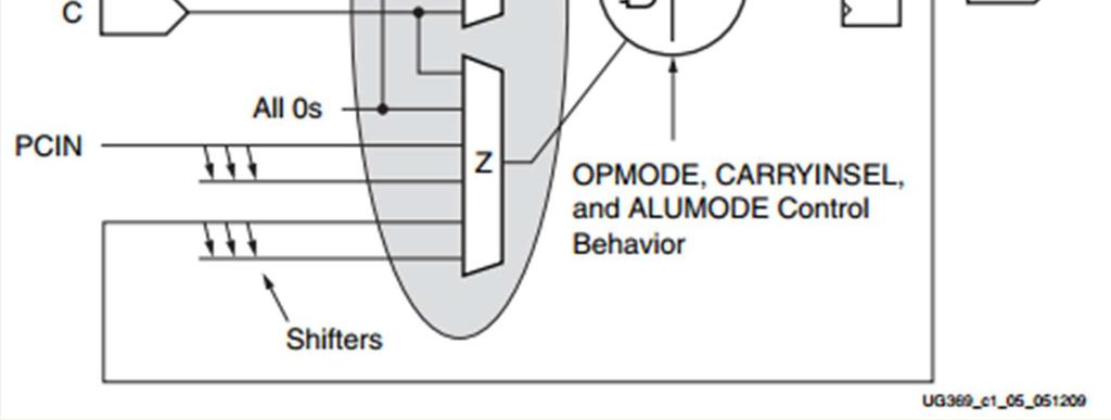
6 DSP48 Slice 4 main control signals: INMODE (5b) controls pre-adders and input registers OPMODE (7b) controls X, Y, Z multiplexers CARRYINSEL (3b) controls source of carry for the final ALU ALUMODE (4b) controls ALU function Each has positive clock-enable, synchronous positive reset (OPMODE and CARRYINSEL share control signals)
7 DSP48 Slice: Input Preadder Block Preadder on A, D inputs Pipeline registers
8 DSP48 Slice: Input Pipeline Block Pipeline on on B input

9 DSP48E1 Slice: Multiplexers
10 DSP48E1 Slice: ALU 2 Modes: 3-input and 2-input 3-Input mode (arithmetic): ALUMODE Function 4 d0 X+Y+Z+CIN 4 d1 X+Y+CIN-Z-1 4 d2 -X-Y-Z-CIN-1 4 d3 Z-(X+Y+CIN) 2-Input mode (logic): 16 logic functions between X and Z
11 DSP48E1 Slice: ALU Arithmetic can be segmented into 2 or 4 SIMD
12 HDL Guide to Multipliers Described using multiplication operator ( * ) Can be combinatorial or registered Implemented as fabric (LUTs) or DSP48 slices based on operand size Per-device thresholds Virtex-7: 6x6 bit multiplier in fabric, larger in DSP48 DSP48 multiplication is natively signed 18x25 bit signed multiplication 17x24 unsigned multiplication (sign bit set to zero)
13 HDL Guide to Multipliers Pipeline registers can be absorbed into the DSP48 slice Up to 2 output pipeline levels Control signals: synchronous positive reset, positive enable clock) begin if(reset) begin result_r1 <= 0; result_r2 <= 0; end else if(en) begin result_r1 <= op_a * op_b; result_r2 <= result_r1; end end
14 HDL Guide to Multipliers Preadd-multipliers clock) if(reset) if(en) begin preadd <= op_b + op_c; result_r1 <= op_a * preadd; result_r2 <= result_r1; end Adder, multiplier and all pipeline stages absorbed into a DSP48 slice Same result for pre-subtraction
15 HDL Guide to Multipliers Preaddsub-multipliers (?) clock) if(reset) begin mult_in_preadd <= 0; result_r1 <= 0; result_r2 <= 0; end else if(en) begin if(paddsub) mult_in_preadd <= op_b - op_c; else mult_in_preadd <= op_b + op_c; result_r1 <= op_a * mult_in_preadd; result_r2 <= result_r1; end
16 HDL Guide to Multipliers Preaddsub-multipliers B and C operands do not exceed 25 bits Paddsub control signal selects subtraction when high (fabric inverter inserted if not) Optionally, a clock-enabled register on paddsub input can be absorbed to improve timing Because paddsub controls part of the INMODE register in the DSP48 slice, and INMODE is reset as a whole, reset is not available for paddsub only Use of reset will result in fabric Flip-Flop for paddsub Clock-enable can be dedicated
17 HDL Guide to MAC Multiply-accumulate block with pre-adder Multiplication result can be accumulated into 48- bit result output 32 samples accumulation at maximum multiplication operand size (32-stage FIR) Related function: preaddsub-multiplypostaddsub multiplier output added or subtracted from 48-bit input Switching operands results in fabric postaddsub Postaddsub control signals same as preaddsub
 Slow speed (fmax) Consumes Resources Wastes Power 8-input adder tree (48b): ~4ns delay and")
18 HDL Guide to DSP48 Adder Cascades Adder trees can only be implemented in fabric Asymptotically optimal delay O(logN) Slow speed (fmax) Consumes Resources Wastes Power 8-input adder tree (48b): ~4ns delay and 336 LUTs
19 HDL Guide to DSP48 Adder Cascades Adder cascades Non-optimal delay O(N) Fast speed (fmax) Requires only DSP48 resources 8-input, 48b adder tree converts to 7-stage adder ~10ns delay (7 DSP48 slices)
20 HDL Guide to DSP48 Barrel Shifters Traditional way to code barrel shifter: assign sh = (input << amount) (input >> amount) 16-bit input results in 48-LUT implementation Idea: use shift-by-multiply: assign mult = input * (1 << amount) assign sh = mult[15:0] mult[31:16] Implemented using 1 DSP48 and 32 LUTs If amount is already decoded: 1 DSP48, 16 LUTs
21 HDL Guide to DSP48 Barrel Shifters Eliminate LUTs by using DSP48 built-in wire shift and adders

22 HDL Guide to DSP48 Barrel Shifters Implement in single DSP48 slice using multiply-accumulate and time multiplexing
23 Exercise: Complex Number Multiplier X = a + bj Y = c + dj using DSP48 Slices Compute X*Y and report resource utilization, fmax
24 Further Reading Virtex-4 FPGA XtremeDSP User Guide 7-Series FPGA DSP Resources User Guide DSP: Designing for Optimal Results
Parallel FIR Filters. Chapter 5
 Chapter 5 Parallel FIR Filters This chapter describes the implementation of high-performance, parallel, full-precision FIR filters using the DSP48 slice in a Virtex-4 device. ecause the Virtex-4 architecture
FPGA Architecture Overview. Generic FPGA Architecture (1) FPGA Architecture
 FPGA Architecture") FPGA Architecture Overview dr chris dick dsp chief architect wireless and signal processing group xilinx inc. Generic FPGA Architecture () Generic FPGA architecture consists of an array of logic tiles
FPGA Architecture Overview dr chris dick dsp chief architect wireless and signal processing group xilinx inc. Generic FPGA Architecture () Generic FPGA architecture consists of an array of logic tiles
TSEA44 - Design for FPGAs
 2015-11-24 Now for something else... Adapting designs to FPGAs Why? Clock frequency Area Power Target FPGA architecture: Xilinx FPGAs with 4 input LUTs (such as Virtex-II) Determining the maximum frequency
Xilinx ASMBL Architecture
 FPGA Structure Xilinx ASMBL Architecture Design Flow Synthesis: HDL to FPGA primitives Translate: FPGA Primitives to FPGA Slice components Map: Packing of Slice components into Slices, placement of Slices
FPGA architecture and design technology
 CE 435 Embedded Systems Spring 2017 FPGA architecture and design technology Nikos Bellas Computer and Communications Engineering Department University of Thessaly 1 FPGA fabric A generic island-style FPGA
Hoplite-DSP Harnessing the Xilinx DSP48 Multiplexers to efficiently support NoCs on FPGAs. Chethan Kumar H B and Nachiket Kapre
 -DSP Harnessing the Xilinx DSP Multiplexers to efficiently support NoCs on FPGAs Chethan Kumar H B and Nachiket Kapre nachiket@ieee.org FPL 201 paper Jan Gray co-author Specs 60 s+100 FFs 2.9ns clock Smallest
IA Digital Electronics - Supervision I
 IA Digital Electronics - Supervision I Nandor Licker Due noon two days before the supervision 1 Overview The goal of this exercise is to design an 8-digit calculator capable of adding
Altera FLEX 8000 Block Diagram
 Altera FLEX 8000 Block Diagram Figure from Altera technical literature FLEX 8000 chip contains 26 162 LABs Each LAB contains 8 Logic Elements (LEs), so a chip contains 208 1296 LEs, totaling 2,500 16,000
Basic FPGA Architectures. Actel FPGAs. PLD Technologies: Antifuse. 3 Digital Systems Implementation Programmable Logic Devices
 3 Digital Systems Implementation Programmable Logic Devices Basic FPGA Architectures Why Programmable Logic Devices (PLDs)? Low cost, low risk way of implementing digital circuits as application specific
ECE 645: Lecture 1. Basic Adders and Counters. Implementation of Adders in FPGAs
 ECE 645: Lecture Basic Adders and Counters Implementation of Adders in FPGAs Required Reading Behrooz Parhami, Computer Arithmetic: Algorithms and Hardware Design Chapter 5, Basic Addition and Counting,
Topics. Midterm Finish Chapter 7
 Lecture 9 Topics Midterm Finish Chapter 7 Xilinx FPGAs Chapter 7 Spartan 3E Architecture Source: Spartan-3E FPGA Family Datasheet CLB Configurable Logic Blocks Each CLB contains four slices Each slice
Digital Circuit Design and Language. Datapath Design. Chang, Ik Joon Kyunghee University
 Digital Circuit Design and Language Datapath Design Chang, Ik Joon Kyunghee University Typical Synchronous Design + Control Section : Finite State Machine + Data Section: Adder, Multiplier, Shift Register
Block RAM. Size. Ports. Virtex-4 and older: 18Kb Virtex-5 and newer: 36Kb, can function as two 18Kb blocks
 Block RAM Dedicated FPGA resource, separate columns from CLBs Designed to implement large (Kb) memories Multi-port capabilities Multi-clock capabilities FIFO capabilities Built-in error detection and correction
Each DSP includes: 3-input, 48-bit adder/subtractor
 Virtex-4 DSP Architecture 2 2 DSP slices per tile 16-256 tiles in 1-8 columns Each DSP includes: 3-input, 48-bit adder/subtractor P P = Z±(X+Y+Cin) Optional accum reg C (48) 18x18-bit 2's-comp multiplier
UNIT-III REGISTER TRANSFER LANGUAGE AND DESIGN OF CONTROL UNIT
 UNIT-III 1 KNREDDY UNIT-III REGISTER TRANSFER LANGUAGE AND DESIGN OF CONTROL UNIT Register Transfer: Register Transfer Language Register Transfer Bus and Memory Transfers Arithmetic Micro operations Logic
Let s put together a Manual Processor
 Lecture 14 Let s put together a Manual Processor Hardware Lecture 14 Slide 1 The processor Inside every computer there is at least one processor which can take an instruction, some operands and produce
Basic FPGA Architecture Xilinx, Inc. All Rights Reserved
 Basic FPGA Architecture 2005 Xilinx, Inc. All Rights Reserved Objectives After completing this module, you will be able to: Identify the basic architectural resources of the Virtex -II FPGA List the differences
Review from last time. CS152 Computer Architecture and Engineering Lecture 6. Verilog (finish) Multiply, Divide, Shift
 Multiply, Divide, Shift") Review from last time CS152 Computer Architecture and Engineering Lecture 6 Verilog (finish) Multiply, Divide, Shift February 11, 2004 John Kubiatowicz (www.cs.berkeley.edu/~kubitron) lecture slides: http://www-inst.eecs.berkeley.edu/~cs152/
Review from last time CS152 Computer Architecture and Engineering Lecture 6 Verilog (finish) Multiply, Divide, Shift February 11, 2004 John Kubiatowicz (www.cs.berkeley.edu/~kubitron) lecture slides: http://www-inst.eecs.berkeley.edu/~cs152/
INTRODUCTION TO FPGA ARCHITECTURE
 3/3/25 INTRODUCTION TO FPGA ARCHITECTURE DIGITAL LOGIC DESIGN (BASIC TECHNIQUES) a b a y 2input Black Box y b Functional Schematic a b y a b y a b y 2 Truth Table (AND) Truth Table (OR) Truth Table (XOR)
FPGA Design Challenge :Techkriti 14 Digital Design using Verilog Part 1
 FPGA Design Challenge :Techkriti 14 Digital Design using Verilog Part 1 Anurag Dwivedi Digital Design : Bottom Up Approach Basic Block - Gates Digital Design : Bottom Up Approach Gates -> Flip Flops Digital
The DSP Primer 8. FPGA Technology. DSPprimer Home. DSPprimer Notes. August 2005, University of Strathclyde, Scotland, UK
 The DSP Primer 8 FPGA Technology Return DSPprimer Home Return DSPprimer Notes August 2005, University of Strathclyde, Scotland, UK For Academic Use Only THIS SLIDE IS BLANK August 2005, For Academic Use
Digital Design with FPGAs. By Neeraj Kulkarni
 Digital Design with FPGAs By Neeraj Kulkarni Some Basic Electronics Basic Elements: Gates: And, Or, Nor, Nand, Xor.. Memory elements: Flip Flops, Registers.. Techniques to design a circuit using basic
CHAPTER 4. DIGITAL DOWNCONVERTER FOR WiMAX SYSTEM
 CHAPTER 4 IMPLEMENTATION OF DIGITAL UPCONVERTER AND DIGITAL DOWNCONVERTER FOR WiMAX SYSTEM 4.1 Introduction FPGAs provide an ideal implementation platform for developing broadband wireless systems such
The Nios II Family of Configurable Soft-core Processors
 The Nios II Family of Configurable Soft-core Processors James Ball August 16, 2005 2005 Altera Corporation Agenda Nios II Introduction Configuring your CPU FPGA vs. ASIC CPU Design Instruction Set Architecture
Using Library Modules in Verilog Designs
 Using Library Modules in Verilog Designs This tutorial explains how Altera s library modules can be included in Verilog-based designs, which are implemented by using the Quartus R II software. Contents:
REGISTER TRANSFER LANGUAGE
 REGISTER TRANSFER LANGUAGE The operations executed on the data stored in the registers are called micro operations. Classifications of micro operations Register transfer micro operations Arithmetic micro
Design of Embedded DSP Processors
 Design of Embedded DSP Processors Unit 3: Microarchitecture, Register file, and ALU 9/11/2017 Unit 3 of TSEA26-2017 H1 1 Contents 1. Microarchitecture and its design 2. Hardware design fundamentals 3.
Stratix II vs. Virtex-4 Performance Comparison
 White Paper Stratix II vs. Virtex-4 Performance Comparison Altera Stratix II devices use a new and innovative logic structure called the adaptive logic module () to make Stratix II devices the industry
Intel Stratix 10 Variable Precision DSP Blocks User Guide
 Intel Stratix 10 Variable Precision DSP Blocks User Guide Updated for Intel Quartus Prime Design Suite: 17.1 Subscribe Send Feedback Latest document on the web: PDF HTML Contents Contents 1 Intel Stratix
EECS150 - Digital Design Lecture 5 - Verilog Logic Synthesis
 EECS150 - Digital Design Lecture 5 - Verilog Logic Synthesis Jan 31, 2012 John Wawrzynek Spring 2012 EECS150 - Lec05-verilog_synth Page 1 Outline Quick review of essentials of state elements Finite State
Binary Adders. Ripple-Carry Adder
 Ripple-Carry Adder Binary Adders x n y n x y x y c n FA c n - c 2 FA c FA c s n MSB position Longest delay (Critical-path delay): d c(n) = n d carry = 2n gate delays d s(n-) = (n-) d carry +d sum = 2n
A SIMULINK-TO-FPGA MULTI-RATE HIERARCHICAL FIR FILTER DESIGN
 A SIMULINK-TO-FPGA MULTI-RATE HIERARCHICAL FIR FILTER DESIGN Xiaoying Li 1 Fuming Sun 2 Enhua Wu 1, 3 1 University of Macau, Macao, China 2 University of Science and Technology Beijing, Beijing, China
Achieving Breakthrough Performance with Virtex-4, the World s Fastest FPGA
 Achieving Breakthrough Performance with Virtex-4, the World s Fastest FPGA Xilinx 90nm Design Seminar Series: Part I Xilinx - #1 in 90 nm We Asked our Customers: What are your challenges? Shorter design
Virtex-II Architecture
 Virtex-II Architecture Block SelectRAM resource I/O Blocks (IOBs) edicated multipliers Programmable interconnect Configurable Logic Blocks (CLBs) Virtex -II architecture s core voltage operates at 1.5V
Arithmetic Circuits. Nurul Hazlina Adder 2. Multiplier 3. Arithmetic Logic Unit (ALU) 4. HDL for Arithmetic Circuit
 4. HDL for Arithmetic Circuit") Nurul Hazlina 1 1. Adder 2. Multiplier 3. Arithmetic Logic Unit (ALU) 4. HDL for Arithmetic Circuit Nurul Hazlina 2 Introduction 1. Digital circuits are frequently used for arithmetic operations 2. Fundamental
Nurul Hazlina 1 1. Adder 2. Multiplier 3. Arithmetic Logic Unit (ALU) 4. HDL for Arithmetic Circuit Nurul Hazlina 2 Introduction 1. Digital circuits are frequently used for arithmetic operations 2. Fundamental
Synthesis Options FPGA and ASIC Technology Comparison - 1
 Synthesis Options Comparison - 1 2009 Xilinx, Inc. All Rights Reserved Welcome If you are new to FPGA design, this module will help you synthesize your design properly These synthesis techniques promote
RUN-TIME RECONFIGURABLE IMPLEMENTATION OF DSP ALGORITHMS USING DISTRIBUTED ARITHMETIC. Zoltan Baruch
 RUN-TIME RECONFIGURABLE IMPLEMENTATION OF DSP ALGORITHMS USING DISTRIBUTED ARITHMETIC Zoltan Baruch Computer Science Department, Technical University of Cluj-Napoca, 26-28, Bariţiu St., 3400 Cluj-Napoca,
Lecture 7. Standard ICs FPGA (Field Programmable Gate Array) VHDL (Very-high-speed integrated circuits. Hardware Description Language)
 VHDL (Very-high-speed integrated circuits. Hardware Description Language)") Standard ICs FPGA (Field Programmable Gate Array) VHDL (Very-high-speed integrated circuits Hardware Description Language) 1 Standard ICs PLD: Programmable Logic Device CPLD: Complex PLD FPGA: Field Programmable
Standard ICs FPGA (Field Programmable Gate Array) VHDL (Very-high-speed integrated circuits Hardware Description Language) 1 Standard ICs PLD: Programmable Logic Device CPLD: Complex PLD FPGA: Field Programmable
Topics. Midterm Finish Chapter 7
 Lecture 9 Topics Midterm Finish Chapter 7 ROM (review) Memory device in which permanent binary information is stored. Example: 32 x 8 ROM Five input lines (2 5 = 32) 32 outputs, each representing a memory
CS429: Computer Organization and Architecture
 CS429: Computer Organization and Architecture Dr. Bill Young Department of Computer Sciences University of Texas at Austin Last updated: January 2, 2018 at 11:23 CS429 Slideset 5: 1 Topics of this Slideset
Using Library Modules in Verilog Designs. 1 Introduction. For Quartus II 13.0
 Using Library Modules in Verilog Designs For Quartus II 13.0 1 Introduction This tutorial explains how Altera s library modules can be included in Verilog-based designs, which are implemented by using
Field Programmable Gate Array (FPGA)
") Field Programmable Gate Array (FPGA) Lecturer: Krébesz, Tamas 1 FPGA in general Reprogrammable Si chip Invented in 1985 by Ross Freeman (Xilinx inc.) Combines the advantages of ASIC and uc-based systems
Field Programmable Gate Array (FPGA) Lecturer: Krébesz, Tamas 1 FPGA in general Reprogrammable Si chip Invented in 1985 by Ross Freeman (Xilinx inc.) Combines the advantages of ASIC and uc-based systems
COSC 243. Computer Architecture 1. COSC 243 (Computer Architecture) Lecture 6 - Computer Architecture 1 1
 Lecture 6 - Computer Architecture 1 1") COSC 243 Computer Architecture 1 COSC 243 (Computer Architecture) Lecture 6 - Computer Architecture 1 1 Overview Last Lecture Flip flops This Lecture Computers Next Lecture Instruction sets and addressing
COSC 243 Computer Architecture 1 COSC 243 (Computer Architecture) Lecture 6 - Computer Architecture 1 1 Overview Last Lecture Flip flops This Lecture Computers Next Lecture Instruction sets and addressing
Chapter 5. Digital Design and Computer Architecture, 2 nd Edition. David Money Harris and Sarah L. Harris. Chapter 5 <1>
 Chapter 5 Digital Design and Computer Architecture, 2 nd Edition David Money Harris and Sarah L. Harris Chapter 5 Chapter 5 :: Topics Introduction Arithmetic Circuits umber Systems Sequential Building
Qsys and IP Core Integration
 Qsys and IP Core Integration Stephen A. Edwards (after David Lariviere) Columbia University Spring 2016 IP Cores Altera s IP Core Integration Tools Connecting IP Cores IP Cores Cyclone V SoC: A Mix of
The Xilinx XC6200 chip, the software tools and the board development tools
 The Xilinx XC6200 chip, the software tools and the board development tools What is an FPGA? Field Programmable Gate Array Fully programmable alternative to a customized chip Used to implement functions
HDL Coding Style Xilinx, Inc. All Rights Reserved
 HDL Coding Style Objective After completing this module, you will be able to: Select a proper coding style to create efficient FPGA designs Specify Xilinx resources that need to be instantiated for various
Writing Circuit Descriptions 8
 8 Writing Circuit Descriptions 8 You can write many logically equivalent descriptions in Verilog to describe a circuit design. However, some descriptions are more efficient than others in terms of the
The Need of Datapath or Register Transfer Logic. Number 1 Number 2 Number 3 Number 4. Numbers from 1 to million. Register
 The Need of Datapath or Register Transfer Logic Number 1 Number 2 Number 3 Number 4 Numbers from 1 to million Register (a) (b) Circuits to add several numbers: (a) combinational circuit to add four numbers;
This document is downloaded from DR-NTU, Nanyang Technological University Library, Singapore.
 This document is downloaded from DR-NTU, Nanyang Technological University Library, Singapore. Title Architecture and application-aware management of complexity of mapping multiplication to FPGA DSP blocks
HIGH-PERFORMANCE RECONFIGURABLE FIR FILTER USING PIPELINE TECHNIQUE
 HIGH-PERFORMANCE RECONFIGURABLE FIR FILTER USING PIPELINE TECHNIQUE Anni Benitta.M #1 and Felcy Jeba Malar.M *2 1# Centre for excellence in VLSI Design, ECE, KCG College of Technology, Chennai, Tamilnadu
EXPERIMENT NUMBER 11 REGISTERED ALU DESIGN
 11-1 EXPERIMENT NUMBER 11 REGISTERED ALU DESIGN Purpose Extend the design of the basic four bit adder to include other arithmetic and logic functions. References Wakerly: Section 5.1 Materials Required
The Next Generation 65-nm FPGA. Steve Douglass, Kees Vissers, Peter Alfke Xilinx August 21, 2006
 The Next Generation 65-nm FPGA Steve Douglass, Kees Vissers, Peter Alfke Xilinx August 21, 2006 Hot Chips, 2006 Structure of the talk 65nm technology going towards 32nm Virtex-5 family Improved I/O Benchmarking
Computer Arithmetic Multiplication & Shift Chapter 3.4 EEC170 FQ 2005
 Computer Arithmetic Multiplication & Shift Chapter 3.4 EEC170 FQ 200 Multiply We will start with unsigned multiply and contrast how humans and computers multiply Layout 8-bit 8 Pipelined Multiplier 1 2
Course Overview Revisited
 Course Overview Revisited void blur_filter_3x3( Image &in, Image &blur) { // allocate blur array Image blur(in.width(), in.height()); // blur in the x dimension for (int y = ; y < in.height(); y++) for
Batchu Jeevanarani and Thota Sreenivas Department of ECE, Sri Vasavi Engg College, Tadepalligudem, West Godavari (DT), Andhra Pradesh, India
, Andhra Pradesh, India") Memory-Based Realization of FIR Digital Filter by Look-Up- Table Optimization Batchu Jeevanarani and Thota Sreenivas Department of ECE, Sri Vasavi Engg College, Tadepalligudem, West Godavari (DT), Andhra
Memory-Based Realization of FIR Digital Filter by Look-Up- Table Optimization Batchu Jeevanarani and Thota Sreenivas Department of ECE, Sri Vasavi Engg College, Tadepalligudem, West Godavari (DT), Andhra
Two hours - online EXAM PAPER MUST NOT BE REMOVED FROM THE EXAM ROOM UNIVERSITY OF MANCHESTER SCHOOL OF COMPUTER SCIENCE
 COMP 12111 Two hours - online This paper version is made available as a backup In this event, only MCQ answers written in the boxes on the exam paper will be marked. EXAM PAPER MUST NOT BE REMOVED FROM
Digital Design with SystemVerilog
 Digital Design with SystemVerilog Prof. Stephen A. Edwards Columbia University Spring 25 Synchronous Digital Design Combinational Logic Sequential Logic Summary of Modeling Styles Testbenches Why HDLs?
Outline. EEL-4713 Computer Architecture Multipliers and shifters. Deriving requirements of ALU. MIPS arithmetic instructions
 Outline EEL-4713 Computer Architecture Multipliers and shifters Multiplication and shift registers Chapter 3, section 3.4 Next lecture Division, floating-point 3.5 3.6 EEL-4713 Ann Gordon-Ross.1 EEL-4713
Figure 1: Verilog used to generate divider
 Abstract Compared to other arithmetic operations, division is not simple or quick in hardware. Division typically requires significantly more hardware to implement when compared to other arithmetic operations.
UNIT - V MEMORY P.VIDYA SAGAR ( ASSOCIATE PROFESSOR) Department of Electronics and Communication Engineering, VBIT
 Department of Electronics and Communication Engineering, VBIT") UNIT - V MEMORY P.VIDYA SAGAR ( ASSOCIATE PROFESSOR) contents Memory: Introduction, Random-Access memory, Memory decoding, ROM, Programmable Logic Array, Programmable Array Logic, Sequential programmable
UNIT - V MEMORY P.VIDYA SAGAR ( ASSOCIATE PROFESSOR) contents Memory: Introduction, Random-Access memory, Memory decoding, ROM, Programmable Logic Array, Programmable Array Logic, Sequential programmable
Counters, Timers and Real-Time Clock
 Introduction In the previous lab, you learned how the Architectural Wizard can be used to generate a desired clock frequency and how the IP Catalog can be used to generate various cores including counters.
CSE140L: Components and Design Techniques for Digital Systems Lab
 CSE140L: Components and Design Techniques for Digital Systems Lab Tajana Simunic Rosing Source: Vahid, Katz, Culler 1 Announcements & Outline Lab 4 due; demo signup times listed on the cse140l site Check
INTRODUCTION TO FIELD PROGRAMMABLE GATE ARRAYS (FPGAS)
") INTRODUCTION TO FIELD PROGRAMMABLE GATE ARRAYS (FPGAS) Bill Jason P. Tomas Dept. of Electrical and Computer Engineering University of Nevada Las Vegas FIELD PROGRAMMABLE ARRAYS Dominant digital design
INTRODUCTION TO FIELD PROGRAMMABLE GATE ARRAYS (FPGAS) Bill Jason P. Tomas Dept. of Electrical and Computer Engineering University of Nevada Las Vegas FIELD PROGRAMMABLE ARRAYS Dominant digital design
FPGAs: FAST TRACK TO DSP
 FPGAs: FAST TRACK TO DSP Revised February 2009 ABSRACT: Given the prevalence of digital signal processing in a variety of industry segments, several implementation solutions are available depending on
Virtex-II Architecture. Virtex II technical, Design Solutions. Active Interconnect Technology (continued)
") Virtex-II Architecture SONET / SDH Virtex II technical, Design Solutions PCI-X PCI DCM Distri RAM 18Kb BRAM Multiplier LVDS FIFO Shift Registers BLVDS SDRAM QDR SRAM Backplane Rev 4 March 4th. 2002 J-L
Virtex-II Architecture SONET / SDH Virtex II technical, Design Solutions PCI-X PCI DCM Distri RAM 18Kb BRAM Multiplier LVDS FIFO Shift Registers BLVDS SDRAM QDR SRAM Backplane Rev 4 March 4th. 2002 J-L
Design and Simulation of Pipelined Double Precision Floating Point Adder/Subtractor and Multiplier Using Verilog
 Design and Simulation of Pipelined Double Precision Floating Point Adder/Subtractor and Multiplier Using Verilog Onkar Singh (1) Kanika Sharma (2) Dept. ECE, Arni University, HP (1) Dept. ECE, NITTTR Chandigarh
Synthesis vs. Compilation Descriptions mapped to hardware Verilog design patterns for best synthesis. Spring 2007 Lec #8 -- HW Synthesis 1
 Verilog Synthesis Synthesis vs. Compilation Descriptions mapped to hardware Verilog design patterns for best synthesis Spring 2007 Lec #8 -- HW Synthesis 1 Logic Synthesis Verilog and VHDL started out
05 - Microarchitecture, RF and ALU
 September 15, 2015 Microarchitecture Design Step 1: Partition each assembly instruction into microoperations, allocate each microoperation into corresponding hardware modules. Step 2: Collect all microoperations
EE 8217 *Reconfigurable Computing Systems Engineering* Sample of Final Examination
 1 Student name: Date: June 26, 2008 General requirements for the exam: 1. This is CLOSED BOOK examination; 2. No questions allowed within the examination period; 3. If something is not clear in question
COPROCESSOR APPROACH TO ACCELERATING MULTIMEDIA APPLICATION [CLAUDIO BRUNELLI, JARI NURMI ] Processor Design
![COPROCESSOR APPROACH TO ACCELERATING MULTIMEDIA APPLICATION [CLAUDIO BRUNELLI, JARI NURMI ] Processor Design](/thumbs/80/81947289.jpg "COPROCESSOR APPROACH TO ACCELERATING MULTIMEDIA APPLICATION [CLAUDIO BRUNELLI, JARI NURMI ] Processor Design") COPROCESSOR APPROACH TO ACCELERATING MULTIMEDIA APPLICATION [CLAUDIO BRUNELLI, JARI NURMI ] Processor Design Lecture Objectives Background Need for Accelerator Accelerators and different type of parallelizm
COPROCESSOR APPROACH TO ACCELERATING MULTIMEDIA APPLICATION [CLAUDIO BRUNELLI, JARI NURMI ] Processor Design Lecture Objectives Background Need for Accelerator Accelerators and different type of parallelizm
CSE140L: Components and Design
 CSE140L: Components and Design Techniques for Digital Systems Lab Tajana Simunic Rosing Source: Vahid, Katz, Culler 1 Grade distribution: 70% Labs 35% Lab 4 30% Lab 3 20% Lab 2 15% Lab 1 30% Final exam
COMPUTER ARCHITECTURE AND ORGANIZATION Register Transfer and Micro-operations 1. Introduction A digital system is an interconnection of digital
 Register Transfer and Micro-operations 1. Introduction A digital system is an interconnection of digital hardware modules that accomplish a specific information-processing task. Digital systems vary in
FPGA Matrix Multiplier
 FPGA Matrix Multiplier In Hwan Baek Henri Samueli School of Engineering and Applied Science University of California Los Angeles Los Angeles, California Email: chris.inhwan.baek@gmail.com David Boeck Henri
CSCB58 - Lab 3. Prelab /3 Part I (in-lab) /2 Part II (in-lab) /2 TOTAL /8
 /2 Part II (in-lab) /2 TOTAL /8") CSCB58 - Lab 3 Latches, Flip-flops, and Registers Learning Objectives The purpose of this exercise is to investigate the fundamental synchronous logic elements: latches, flip-flops, and registers. Prelab
CSCB58 - Lab 3 Latches, Flip-flops, and Registers Learning Objectives The purpose of this exercise is to investigate the fundamental synchronous logic elements: latches, flip-flops, and registers. Prelab
Implementation of DSP Algorithms
 Implementation of DSP Algorithms Main frame computers Dedicated (application specific) architectures Programmable digital signal processors voice band data modem speech codec 1 PDSP and General-Purpose
Digital Logic & Computer Design CS Professor Dan Moldovan Spring 2010
 Digital Logic & Computer Design CS 434 Professor Dan Moldovan Spring 2 Copyright 27 Elsevier 5- Chapter 5 :: Digital Building Blocks Digital Design and Computer Architecture David Money Harris and Sarah
Design and Implementation of IEEE-754 Decimal Floating Point Adder, Subtractor and Multiplier
 International Journal of Engineering and Advanced Technology (IJEAT) ISSN: 2249 8958, Volume-4 Issue 1, October 2014 Design and Implementation of IEEE-754 Decimal Floating Point Adder, Subtractor and Multiplier
ESE532: System-on-a-Chip Architecture. Today. Message. Graph Cycles. Preclass 1. Reminder
 ESE532: System-on-a-Chip Architecture Day 8: September 26, 2018 Spatial Computations Today Graph Cycles (from Day 7) Accelerator Pipelines FPGAs Zynq Computational Capacity 1 2 Message Custom accelerators
Tailoring the 32-Bit ALU to MIPS
 Tailoring the 32-Bit ALU to MIPS MIPS ALU extensions Overflow detection: Carry into MSB XOR Carry out of MSB Branch instructions Shift instructions Slt instruction Immediate instructions ALU performance
Introduction to Field Programmable Gate Arrays
 Introduction to Field Programmable Gate Arrays Lecture 1/3 CERN Accelerator School on Digital Signal Processing Sigtuna, Sweden, 31 May 9 June 2007 Javier Serrano, CERN AB-CO-HT Outline Historical introduction.
EE178 Lecture Module 2. Eric Crabill SJSU / Xilinx Fall 2007
 EE178 Lecture Module 2 Eric Crabill SJSU / Xilinx Fall 2007 Lecture #4 Agenda Survey of implementation technologies. Implementation Technologies Small scale and medium scale integration. Up to about 200
EEL 4783: HDL in Digital System Design
 EEL 4783: HDL in Digital System Design Lecture 15: Logic Synthesis with Verilog Prof. Mingjie Lin 1 Verilog Synthesis Synthesis vs. Compilation Descriptions mapped to hardware Verilog design patterns for
Lecture 3: Modeling in VHDL. EE 3610 Digital Systems
 EE 3610: Digital Systems 1 Lecture 3: Modeling in VHDL VHDL: Overview 2 VHDL VHSIC Hardware Description Language VHSIC=Very High Speed Integrated Circuit Programming language for modelling of hardware
FPGA for Complex System Implementation. National Chiao Tung University Chun-Jen Tsai 04/14/2011
 FPGA for Complex System Implementation National Chiao Tung University Chun-Jen Tsai 04/14/2011 About FPGA FPGA was invented by Ross Freeman in 1989 SRAM-based FPGA properties Standard parts Allowing multi-level
4. DSP Blocks in Stratix IV Devices
 4. DSP Blocks in Stratix IV Devices February 2011 SIV51004-3.1 SIV51004-3.1 This chapter describes how the Stratix IV device digital signal processing (DSP) blocks are optimized to support DSP applications
Optimized Design and Implementation of a 16-bit Iterative Logarithmic Multiplier
 Optimized Design and Implementation a 16-bit Iterative Logarithmic Multiplier Laxmi Kosta 1, Jaspreet Hora 2, Rupa Tomaskar 3 1 Lecturer, Department Electronic & Telecommunication Engineering, RGCER, Nagpur,India,
Method We follow- How to Get Entry Pass in SEMICODUCTOR Industries for 3rd year engineering. Winter/Summer Training
 Method We follow- How to Get Entry Pass in SEMICODUCTOR Industries for 3rd year engineering Winter/Summer Training Level 2 continues. 3 rd Year 4 th Year FIG-3 Level 1 (Basic & Mandatory) & Level 1.1 and
Arithmetic Logic Unit. Digital Computer Design
 Arithmetic Logic Unit Digital Computer Design Arithmetic Circuits Arithmetic circuits are the central building blocks of computers. Computers and digital logic perform many arithmetic functions: addition,
Implementation of High Speed FIR Filter using Serial and Parallel Distributed Arithmetic Algorithm
 Volume 25 No.7, July 211 Implementation of High Speed FIR Filter using Serial and Parallel Distriuted Arithmetic Algorithm Narendra Singh Pal Electronics &Communication, Dr.B.R.Amedkar Tecnology, Jalandhar
Organic Computing. Dr. rer. nat. Christophe Bobda Prof. Dr. Rolf Wanka Department of Computer Science 12 Hardware-Software-Co-Design
 Dr. rer. nat. Christophe Bobda Prof. Dr. Rolf Wanka Department of Computer Science 12 Hardware-Software-Co-Design 1 Reconfigurable Computing Platforms 2 The Von Neumann Computer Principle In 1945, the
INTRODUCTION TO CATAPULT C
 INTRODUCTION TO CATAPULT C Vijay Madisetti, Mohanned Sinnokrot Georgia Institute of Technology School of Electrical and Computer Engineering with adaptations and updates by: Dongwook Lee, Andreas Gerstlauer
Today. Comments about assignment Max 1/T (skew = 0) Max clock skew? Comments about assignment 3 ASICs and Programmable logic Others courses
 Max clock skew? Comments about assignment 3 ASICs and Programmable logic Others courses") Today Comments about assignment 3-43 Comments about assignment 3 ASICs and Programmable logic Others courses octor Per should show up in the end of the lecture Mealy machines can not be coded in a single
Today Comments about assignment 3-43 Comments about assignment 3 ASICs and Programmable logic Others courses octor Per should show up in the end of the lecture Mealy machines can not be coded in a single
Agenda. Introduction FPGA DSP platforms Design challenges New programming models for FPGAs
 New Directions in Programming FPGAs for DSP Dr. Jim Hwang Xilinx, Inc. Agenda Introduction FPGA DSP platforms Design challenges New programming models for FPGAs System Generator Getting your math into
System-on Solution from Altera and Xilinx
 System-on on-a-programmable-chip Solution from Altera and Xilinx Xun Yang VLSI CAD Lab, Computer Science Department, UCLA FPGAs with Embedded Microprocessors Combination of embedded processors and programmable
Overview. EECS Components and Design Techniques for Digital Systems. Lec 16 Arithmetic II (Multiplication) Computer Number Systems.
 Computer Number Systems.") Overview EE 15 - omponents and Design Techniques for Digital ystems Lec 16 Arithmetic II (Multiplication) Review of Addition Overflow Multiplication Further adder optimizations for multiplication LA in
Overview EE 15 - omponents and Design Techniques for Digital ystems Lec 16 Arithmetic II (Multiplication) Review of Addition Overflow Multiplication Further adder optimizations for multiplication LA in
High Capacity and High Performance 20nm FPGAs. Steve Young, Dinesh Gaitonde August Copyright 2014 Xilinx
 High Capacity and High Performance 20nm FPGAs Steve Young, Dinesh Gaitonde August 2014 Not a Complete Product Overview Page 2 Outline Page 3 Petabytes per month Increasing Bandwidth Global IP Traffic Growth
Overview. CSE372 Digital Systems Organization and Design Lab. Hardware CAD. Two Types of Chips
 Overview CSE372 Digital Systems Organization and Design Lab Prof. Milo Martin Unit 5: Hardware Synthesis CAD (Computer Aided Design) Use computers to design computers Virtuous cycle Architectural-level,
2015 Paper E2.1: Digital Electronics II
 s 2015 Paper E2.1: Digital Electronics II Answer ALL questions. There are THREE questions on the paper. Question ONE counts for 40% of the marks, other questions 30% Time allowed: 2 hours (Not to be removed
ECE 341 Midterm Exam
 ECE 341 Midterm Exam Time allowed: 90 minutes Total Points: 75 Points Scored: Name: Problem No. 1 (10 points) For each of the following statements, indicate whether the statement is TRUE or FALSE: (a)