Federal Urdu University of Arts, Science and Technology, Islamabad VLSI SYSTEM DESIGN. Prepared By: Engr. Yousaf Hameed.
|
|
|
- Maximillian Holland
- 6 years ago
- Views:
Transcription

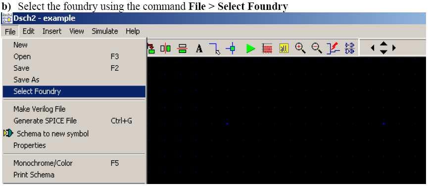
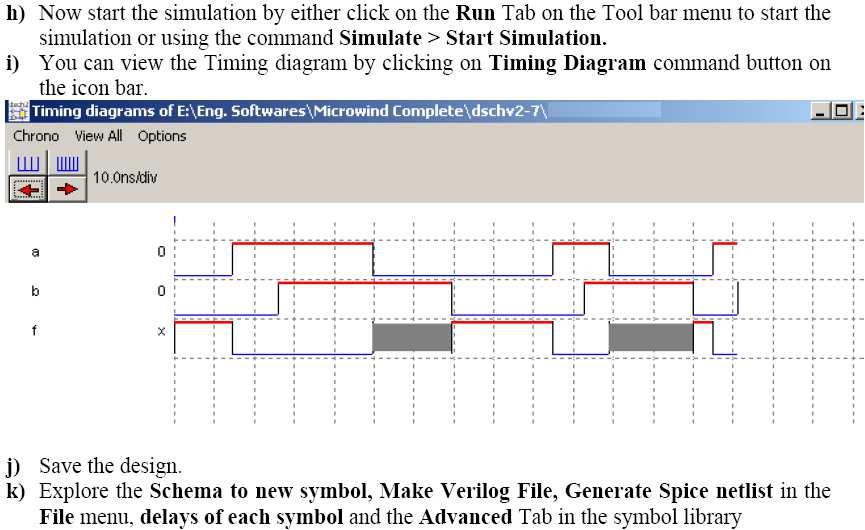
1 VLSI SYSTEM DESIGN Prepared By: Engr. Yousaf Hameed Lab Engineer BASIC ELECTRICAL & DIGITAL SYSTEMS LAB DEPARTMENT OF ELECTRICAL ENGINEERING VLSI System Design 1
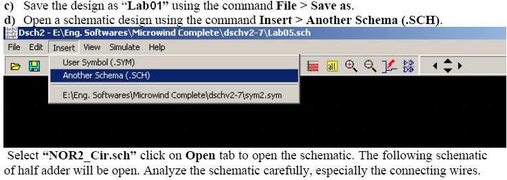
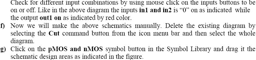
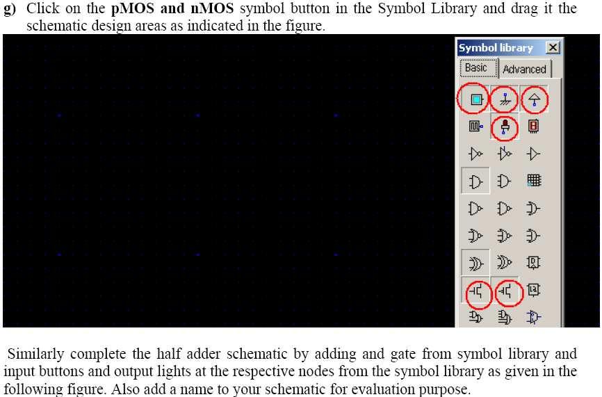
2 LAB 01 Schematic Introduction to DSCH and a simple Gate implementation in DSCH VLSI System Design 2

3 VLSI System Design 3

4 VLSI System Design 4

5 VLSI System Design 5

6 VLSI System Design 6
7 LAB 02 Schematic CMOS Switch Level Modeling of Basic Gates (Nand, Nor, Xor,Xnor) and Complex Function in DSCH. VLSI System Design 7
8 VLSI System Design 8
9 VLSI System Design 9
10 LAB 03 Schematic Implementation of Full adder in DSCH at switch level VLSI System Design 10
11 VLSI System Design 11
12 LAB 04 Layout Introduction to Microwind and analysis of MOSFETS VLSI System Design 12

13 VLSI System Design 13

14 VLSI System Design 14

15 VLSI System Design 15

16 VLSI System Design 16
17 VLSI System Design 17
18 VLSI System Design 18
19 LAB 05 Layout MOSFET Inverter Characteristics and layout in Microwind (Layer Level Modeling) VLSI System Design 19

20 VLSI System Design 20

21 VLSI System Design 21

22 VLSI System Design 22

23 VLSI System Design 23
")
24 LAB 06 Layout Layout of basic gates using 0.25 micron technology in Microwind (Layer level modeling) VLSI System Design 24
25 VLSI System Design 25

26 VLSI System Design 26

27 VLSI System Design 27

28 VLSI System Design 28
29 VLSI System Design 29
30 LAB 07 Layout Layout of Complex gate using 0.25 micron technology in Microwind (Layer level modeling) VLSI System Design 30

31 VLSI System Design 31
32 VLSI System Design 32

33 LAB 08 Layout Design and implementation of full adder at layer level in Microwind. VLSI System Design 33

34 VLSI System Design 34

35 VLSI System Design 35
36 VLSI System Design 36
37 LAB 09 Layout Design and implementation of Static RAM Cell layout using CMOS 0.12 micron technology in Microwind. VLSI System Design 37
38 VLSI System Design 38

39 VLSI System Design 39

40 VLSI System Design 40
.")
41 LAB 10 Introduction to Modelsim (Verilog Coding) implementation of Half Adder & Full Adder at gate level, data flow and behavior level A - GATE LEVEL DESIGN At gate level, the circuit is described in terms of gates (e.g. and, nand). Hardware design at this level is intuitive for a user with a basic knowledge of digital logic design because it is possible to see a one-to-one correspondence between the logic circuit diagram and the Verilog description. Lab Overview In this lab you will: Learn modeling at gate level Half adder design Full adder design Multiplexer design Decoder design Background: The simplest form of adder is called a Half-Adder (HA). The HA performs bit-wise addition between two input bits. Depending on the result of the operation, the HA either sets or clears its Sum and Carry bit. A HA can be expanded to include the logic for carry in, and the modified unit is called the Full Adder (FA). VLSI System Design 41
; reg a,b; wire s,c; HA HA_inst(a,b,s,c); initial begin a=0; b=0; #10 a=0; b=1; #10 a=1; b=0; #10 a=1; b=1; end endmodule VLSI System")
42 The verilog code for the half adder is module HA(a,b,s,c); input a,b; output s,c; xor(s,a,b); and(c,a,b); endmodule The test bench of the half adder is module testbench_ha(); reg a,b; wire s,c; HA HA_inst(a,b,s,c); initial begin a=0; b=0; #10 a=0; b=1; #10 a=1; b=0; #10 a=1; b=1; end endmodule VLSI System Design 42
; input a,b,cin; output s,cout; wire c0, s0, c1; HA HA_inst0(a,b,s0,c0); HA HA_inst1(cin,s0,s,c1); or(cout,")
43 We can use the half adder to design a full adder as shown in figure 1.3. The full adder takes an extra bit as input for carry in. The verilog code of full adder is module FA(a,b,cin,s,cout); input a,b,cin; output s,cout; wire c0, s0, c1; HA HA_inst0(a,b,s0,c0); HA HA_inst1(cin,s0,s,c1); or(cout, c1,c0); endmodule VLSI System Design 43

44 B - DATAFLOW LEVEL DESIGN Dataflow modeling provides a powerful way to implement a design. Verilog allows a circuit to be designed in terms of the data flow between registers and how a design processes data rather than instantiation of individual gates. Lab Overview In this lab you will: Learn modeling at dataflow level Background: Half adder design (dataflow) Full adder design (dataflow) 4-bit adder design 12-bit Carry Select Adder (CSA) Multiplexer design (dataflow) Decoder design (dataflow) The simplest form of adder is called a Half-Adder (HA). The HA performs bit-wise addition between two input bits. Depending on the result of the operation, the HA either sets or clears its Sum and Carry bit. A HA can be expanded to include the logic for carry in, and the modified unit is called the Full Adder (FA). VLSI System Design 44
; reg a,b; wire s,c; HA HA_inst(a,b,s,c); initial begin a=0; b=0; #10 a=0; b=1; #10 a=1; b=0; #10 a=1; b=1; end endmodule VLSI System Design 45")
45 The verilog code for the half adder at dataflow level is module HA(a,b,s,c); input a,b; output s,c; assign s = a^b; assign c = a&b; // assign {s,c} = a+b; endmodule The test bench of the half adder is module testbench_ha(); reg a,b; wire s,c; HA HA_inst(a,b,s,c); initial begin a=0; b=0; #10 a=0; b=1; #10 a=1; b=0; #10 a=1; b=1; end endmodule VLSI System Design 45
46 We can use the half adder to design a full adder as shown in figure 2.3. The full adder takes an extra bit as input for carry in. The verilog code of full adder at dataflow level is module FA(a,b,cin,s,cout); input a,b,cin; output s,cout; wire c0, s0, c1; HA HA_inst0(a,b,s0,c0); HA HA_inst1(cin,s0,s,c1); assign cout = c1 c0; assign {s,cout} = a + b + cin; endmodule VLSI System Design 46
47 C. BEHAVIORAL LEVEL DESIGN With the increasing complexity of digital design, it has become vitally important to make wise design decisions early in a project. Designers need to be able to evaluate the trade-offs of various architectures and algorithms before they decide on the optimum architecture and algorithm to implement in hardware. Thus, architectural evaluation takes place at an algorithmic level where the designers do not necessarily think in terms of logic gates or data flow but in terms of the algorithm they wish to implement in hardware. They are more concerned about the behavior of the algorithm and its performance. Only after the high-level architecture and algorithm are finalized, do designers start focusing on building the digital circuit to implement the algorithm. Verilog provides designers the ability to describe design functionality in an algorithmic manner. In other words, the designer describes the behavior of the circuit. Thus, behavioral modeling represents the circuit at a very high level of abstraction. Lab Overview In this lab you will: Learn modeling at dataflow level Half adder design (dataflow) Full adder design (dataflow) 4-bit adder design 12-bit Carry Select Adder (CSA) Multiplexer design (dataflow) Decoder design (dataflow) Background: The simplest form of adder is called a Half-Adder (HA). The HA performs bit-wise addition between two input bits. Depending on the result of the operation, the HA either sets or clears its Sum and Carry bit. A HA can be expanded to include the logic for carry in, and the modified unit is called the Full Adder (FA). At behavioral level you don t need to know the structural model but you are only concerned with the behavioral of a circuit. Comments have been added in the code which give a feel for behavioral level coding. VLSI System Design 47
; reg a,b; wire s,c; HA HA_inst(a,b,s,c); initial begin a=0; b=0; #10 a=0; b=1; VLSI System Design")
48 The verilog code for the half adder at behavioral level is module HA(a,b,s,c); input a,b; output s,c; reg s,c; or b) begin s= a^b; c = a&b; //OR {s,c} = a+b; end endmodule The test bench of the half adder is module testbench_ha(); reg a,b; wire s,c; HA HA_inst(a,b,s,c); initial begin a=0; b=0; #10 a=0; b=1; VLSI System Design 48
49 #10 a=1; b=0; #10 a=1; b=1; end endmodule You can use the half adder to design a full adder. The full adder takes an extra bit as input for carry in. The Verilog code of full adder at behavioral level is module FA(a,b,cin,s,cout); input a,b,cin; output s,cout; wire c0, s0, c1; HA HA_inst0(a,b,s0,c0); HA HA_inst1(cin,s0,s,c1); assign cout = c1 c0; // OR // or b or cin) //{s,cout} = a+b+cin; endmodule VLSI System Design 49
50 LAB 11 Implementation of 2 to 1 line MUX The Verilog code of 2 to 1 line multiplexer at dataflow level is module mux(i0,i1,selct,m,n,out); input i0,i1,selct; output m,n,out; assign m=i0&selct; assign n=i1&~selct; assign out=m n; endmodule The test bench of 2 to 1 line multiplexer is module testbench_mux; reg i0,i1,selct; wire m,n; mux ff(i0,i1,selct,m,n,out); initial begin i0=1'b0;i1=1'b1;selct=1'b1; //inputs a=0 and b=1 #10 i0=1'b0;i1=1'b1;selct=1'b0; #10 VLSI System Design 50
51 $finish; end endmodule Lab Tasks: 1. Write a verilog code for 2 to 1 line multiplexer in behavioral level 2. Write a verilog code for 4 to 1 line multiplexer in behavioral level. VLSI System Design 51
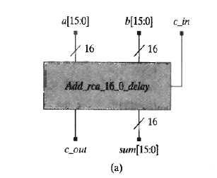
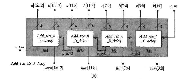
52 Lab 12 Implementation of 16 bit Ripple Carry Adder VLSI System Design 52
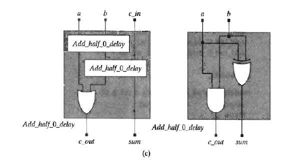
53 DESIGN HIERARCY OF A 16-BIT RIPPLE-CARRY ADDER module Add_rca_16 (sum, c_out, a, b, c_in); output [15: 0] sum; output c_out; input [15: 0] a, b; input c_in; wire c_in4, c_in8, c_in12; Add_rca_4 M4 (sum[3:0], c_in4, a[3:0], b[3:0], c_in); Add_rca_4 M3 (sum[7:4], c_in8, a[7:4], b[7:4], c_in4); Add_rca_4 M2 (sum[11:8], c_in12, a[11:8], b[11:8], c_in8); Add_rca_4 M1 (sum[15:12], c_out, a[15:12], b[15:12], c_in12); endmodule module Add_rca_4 (sum, c_out, a, b, c_in); output [3: 0] sum; output c_out; input [3: 0] a, b; input c_in; wire c_in2, c_in3, c_in4; Add_full M4 (sum[0], c_in2,a[0], b[0], c_in); Add_full M3 (sum[1], c_in3, a[1], b[1], c_in2); VLSI System Design 53
54 Add_full M2 (sum[2], c_in4, a[2], b[2], c_in3); Add_full M1 (sum[3], c_out, a[3], b[3], c_in4); endmodule module Add_full (sum, c_out, a, b, c_in); output sum, c_out; input a, b, c_in; wire w1, w2, w3; Add_half M2 (w1, w2, a, b); Add_half M1 (sum, w3, w1, c_in); or G1 (c_out, w2, w3); endmodule module Add_half (sum, c_out, a, b); output sum, c_out; input a, b; wire c_out_bar; xor M1 (sum, a, b); and M2 (c_out, a, b); endmodule Test Bench module test_add_rca_16 (); wire [15: 0] sum; wire c_out; reg [15: 0] a, b; reg c_in; Add_rca_16 M1 (sum, c_out, a, b, c_in); initial begin #10 a = 16'h0000; b = 16'h0000; c_in = 0; #10 a = 16'h000f; b = 16'h000c; c_in = 0; #10 a = 16'h000f; b = 16'h000c; c_in = 1; #10 a = 16'h0000; b = 16'h0000; c_in = 1; #10 a = 16'h000f; b = 16'h0001; c_in = 0; #10 a = 16'h000f; b = 16'h0001; c_in = 1; $finish; end endmodule VLSI System Design 54
55 LAB 13 SEQUENTIAL CIRCUITS I (FLIP FLOPS) Computers and other digital systems that have memory or that execute a sequence of operations under the direction of stored information are referred to as sequential machines and their circuitry is modeled by sequential logic. Sequential machines do not behave like combinational logic because the outputs of a sequential machine depend on the history of the applied inputs as well as on their present value. The history of the inputs applied to a sequential machine is represented by the state of the machine and requires hardware elements that store information; that is, it requires memory to store the state of the machine as an encoded binary word. Lab Overview In this lab you will: Flip flop designs D_FF JK_FF T_FF Sequential machine design using flip flop Background: There are two main types of sequential circuits and their classification depends on the timing of their signals. 1. A synchronous sequential circuit is a system whose behavior can be defind from the knowledge of its signals at discrete instant of time 2. The behavior of an asynchronous sequential circuit depends upon the input signals at any time and the order in which the inputs change. The storage elements used in clocked sequential circuit are called flip flops. A flip flop is a binary storage device capable of storing one bit of information. The state of a flip flop can change only during a clock pulse transition. Latches are used to model asynchronous circuits. A latch also holds one bit value but the state of the latch can change with changes in inputs and does not require synchronization with clock pulse. In this lab we will learn to model different flip flops using Verilog. D_FF, JK_FF and T_FF are the common flip flops used in synchronous sequential circuits. Function table are used to describe different flip flops. D_FF is the simplest of the flip-flops because its next state is equal to its present state D Table 1 D Flip-Flop Q(t+1) JK_FF has its next state equal to its present state when inputs J and K are both equal to 0. When K=1 and J=0, the clock resets the flip-flop and Q(t+1) = 0. With J=1 and K=0, the flip-flops sets and Q(t+1) =1. When both J and k are equal to 1, the next state changes to the complement of the present state. Table 2 JK Flip-Flop VLSI System Design 55
56 J K Q(t+1) 0 0 Q(t) Q (t+1) T_FF toggles when the T=1 otherwise the state of T_ff does not change. Table 3 T Flip-Flop T Q(t+1) 0 Q(t) 1 Q (t+1) Lab Tasks: 1. Write verilog code for D flip flop and write a test bench to verify the design. 2. Write verilog code for JK flip flop and write a test bench to verify the design. 3. Write verilog code for T flip flop and write a test bench to verify the design. Documentation Submit the codes along with the wave diagrams for the D, JK, T flip flops. VLSI System Design 56
57 LAB 14 SEQUENTIAL CIRCUITS II Unlike combinational logic, whose output is an immediate function of only its present inputs, sequential logic depends on the history of its inputs. This dependency is expressed by the concept of state The future behavior of a sequential machine is completely characterized by its input and its present state. Lab Overview In this lab you will learn: State machines State diagrams State machine design in Verilog Background: Finite State Machines are used to model Sequential circuits since the states of the sequential circuits change depending upon the inputs at the clock edge. A state diagram is used to describe the sequential behavior of the circuit showing the transition of states according to the inputs. Here a traffic light controller example is presented to show the Verilog coding of Finite state machine. Example: Traffic light controller The following specifications must be considered: 1. The traffic signal for the main highway gets highest priority because cars are continuously present on the main highway. Thus, the main highway signal remains green by default. 2. Occasionally, cars from the country road arrive at the traffic signal. The traffic signal for the country road must turn green only long enough to let the cars on the country road go. 3. As soon as there are no cars on the country road, the country road traffic signal turns yellow and then red and the traffic signal on the main highway turn green again. 4. There is a sensor to detect cars waiting on the country road. The sensor sends a signal X as input to the controller. X = 1 if there are cars on the country road; otherwise, X= 0. The state machine diagram and the state definitions for the traffic signal controller are shown in the following figure VLSI System Design 57
; //I/O ports output [1:0] hwy,")
58 Figure 5.2 State diagram Table 5.1 State and output signals The traffic signal controller module can be designed with behavioral Verilog constructs module sig_control (hwy, cntry, X, clock, clear); //I/O ports output [1:0] hwy, cntry; //2-bit output for 3 states of signal //GREEN, YELLOW, RED; reg [1:0] hwy, cntry; //declared output signals are registers input X; //if TRUE, indicates that there is car on //the country road, otherwise FALSE input clock, clear; VLSI System Design 58
59 parameter RED = 2'd0, YELLOW = 2'd1, GREEN = 2'd2; //State definition HWY CNTRY parameter S0 = 3'd0, //GREEN RED S1 = 3'd1, //YELLOW RED S2 = 3'd2, //RED RED S3 = 3'd3, //RED GREEN S4 = 3'd4; //RED YELLOW //Internal state variables reg [2:0] state; reg [2:0] next_state; //state changes only at positive edge of clock clock) if (clear) state <= S0; //Controller starts in S0 state else state <= next_state; //State change //Compute values of main signal and country signal begin hwy = GREEN; //Default Light Assignment for Highway light cntry = RED; //Default Light Assignment for Country light case(state) S0: ; // No change, use default S1: hwy = YELLOW; S2: hwy = RED; S3: begin hwy = RED; cntry = GREEN; end S4: begin hwy = RED; cntry = YELLOW; end endcase end //State machine using case statements or X) VLSI System Design 59
60 begin case (state) S0: if(x) next_state = S1; else next_state = S0; S1: begin next_state = S2; end S2: begin next_state = S3; end S3: if(x) next_state = S3; else next_state = S4; S4: begin next_state = S0; end default: next_state = S0; endcase endmodule Federal Urdu University of Arts, Science and Technology, Islamabad Lab Tasks: 1. Write verilog code. 2. Write a test bench to verify the design Documentation Submit the code along with the wave diagrams for the sequence detector VLSI System Design 60
DIGITAL SYSTEM DESIGN
 DIGITAL SYSTEM DESIGN Prepared By: Engr. Yousaf Hameed Lab Engineer BASIC ELECTRICAL & DIGITAL SYSTEMS LAB DEPARTMENT OF ELECTRICAL ENGINEERING Digital System Design 1 Name: Registration No: Roll No: Semester:
DIGITAL SYSTEM DESIGN
 DIGITAL SYSTEM DESIGN Prepared By: Engr. Yousaf Hameed Lab Engineer BASIC ELECTRICAL & DIGITAL SYSTEMS LAB DEPARTMENT OF ELECTRICAL ENGINEERING Digital System Design 1 Name: Registration No: Roll No: Semester:
Digital Design with FPGAs. By Neeraj Kulkarni
 Digital Design with FPGAs By Neeraj Kulkarni Some Basic Electronics Basic Elements: Gates: And, Or, Nor, Nand, Xor.. Memory elements: Flip Flops, Registers.. Techniques to design a circuit using basic
FPGA Design Challenge :Techkriti 14 Digital Design using Verilog Part 1
 FPGA Design Challenge :Techkriti 14 Digital Design using Verilog Part 1 Anurag Dwivedi Digital Design : Bottom Up Approach Basic Block - Gates Digital Design : Bottom Up Approach Gates -> Flip Flops Digital
Introduction to Verilog design. Design flow (from the book)
") Introduction to Verilog design Lecture 2 ECE 156A 1 Design flow (from the book) ECE 156A 2 1 Hierarchical Design Chip Modules Cells Primitives A chip contain many modules A module may contain other modules
Introduction to Verilog design Lecture 2 ECE 156A 1 Design flow (from the book) ECE 156A 2 1 Hierarchical Design Chip Modules Cells Primitives A chip contain many modules A module may contain other modules
Digital Circuit Design and Language. Datapath Design. Chang, Ik Joon Kyunghee University
 Digital Circuit Design and Language Datapath Design Chang, Ik Joon Kyunghee University Typical Synchronous Design + Control Section : Finite State Machine + Data Section: Adder, Multiplier, Shift Register
N-input EX-NOR gate. N-output inverter. N-input NOR gate
 Hardware Description Language HDL Introduction HDL is a hardware description language used to design and document electronic systems. HDL allows designers to design at various levels of abstraction. It
EPC6055 Digital Integrated Circuits EXAM 1 Fall Semester 2013
 EPC6055 Digital Integrated Circuits EXAM 1 Fall Semester 2013 Print Here Student ID Signature This is a closed book exam. The exam is to be completed in one-hundred ten (110) minutes. Don t use scratch
Sequential Logic Design
 Sequential Logic Design Design of Digital Circuits 2017 Srdjan Capkun Onur Mutlu (Guest starring: Frank K. Gürkaynak and Aanjhan Ranganathan) http://www.syssec.ethz.ch/education/digitaltechnik_17 Adapted
Verilog HDL. Gate-Level Modeling
 Verilog HDL Verilog is a concurrent programming language unlike C, which is sequential in nature. block - executes once at time 0. If there is more then one block, each execute concurrently always block
Introduction to Verilog HDL. Verilog 1
 Introduction to HDL Hardware Description Language (HDL) High-Level Programming Language Special constructs to model microelectronic circuits Describe the operation of a circuit at various levels of abstraction
ACS College of Engineering. Department of Biomedical Engineering. Logic Design Lab pre lab questions ( ) Cycle-1
 Cycle-1") ACS College of Engineering Department of Biomedical Engineering Logic Design Lab pre lab questions (2015-2016) Cycle-1 1. What is a combinational circuit? 2. What are the various methods of simplifying
ACS College of Engineering Department of Biomedical Engineering Logic Design Lab pre lab questions (2015-2016) Cycle-1 1. What is a combinational circuit? 2. What are the various methods of simplifying
Introduction to Verilog design. Design flow (from the book) Hierarchical Design. Lecture 2
 Hierarchical Design. Lecture 2") Introduction to Verilog design Lecture 2 ECE 156A 1 Design flow (from the book) ECE 156A 2 Hierarchical Design Chip Modules Cells Primitives A chip contain many modules A module may contain other modules
Introduction to Verilog design Lecture 2 ECE 156A 1 Design flow (from the book) ECE 156A 2 Hierarchical Design Chip Modules Cells Primitives A chip contain many modules A module may contain other modules
Tutorial on Verilog HDL
 Tutorial on Verilog HDL HDL Hardware Description Languages Widely used in logic design Verilog and VHDL Describe hardware using code Document logic functions Simulate logic before building Synthesize code
Design Using Verilog
 EGC220 Design Using Verilog Baback Izadi Division of Engineering Programs bai@engr.newpaltz.edu Basic Verilog Lexical Convention Lexical convention are close to C++. Comment // to the of the line. /* to
ELCT 501: Digital System Design
 ELCT 501: Digital System Lecture 4: CAD tools (Continued) Dr. Mohamed Abd El Ghany, Basic VHDL Concept Via an Example Problem: write VHDL code for 1-bit adder 4-bit adder 2 1-bit adder Inputs: A (1 bit)
VHDL Examples Mohamed Zaky
 VHDL Examples By Mohamed Zaky (mz_rasmy@yahoo.co.uk) 1 Half Adder The Half Adder simply adds 2 input bits, to produce a sum & carry output. Here we want to add A + B to produce Sum (S) and carry (C). A
Synthesizable Verilog
 Synthesizable Verilog Courtesy of Dr. Edwards@Columbia, and Dr. Franzon@NCSU http://csce.uark.edu +1 (479) 575-6043 yrpeng@uark.edu Design Methodology Structure and Function (Behavior) of a Design HDL
Chap 6 Introduction to HDL (d)
") Design with Verilog Chap 6 Introduction to HDL (d) Credit to: MD Rizal Othman Faculty of Electrical & Electronics Engineering Universiti Malaysia Pahang Ext: 6036 VERILOG HDL Basic Unit A module Module
Design with Verilog Chap 6 Introduction to HDL (d) Credit to: MD Rizal Othman Faculty of Electrical & Electronics Engineering Universiti Malaysia Pahang Ext: 6036 VERILOG HDL Basic Unit A module Module
Advanced Digital Design Using FPGA. Dr. Shahrokh Abadi
 Advanced Digital Design Using FPGA Dr. Shahrokh Abadi 1 Venue Computer Lab: Tuesdays 10 12 am (Fixed) Computer Lab: Wednesday 10-12 am (Every other odd weeks) Note: Due to some unpredicted problems with
Lecture 32: SystemVerilog
 Lecture 32: SystemVerilog Outline SystemVerilog module adder(input logic [31:0] a, input logic [31:0] b, output logic [31:0] y); assign y = a + b; Note that the inputs and outputs are 32-bit busses. 17:
ARM 64-bit Register File
 ARM 64-bit Register File Introduction: In this class we will develop and simulate a simple, pipelined ARM microprocessor. Labs #1 & #2 build some basic components of the processor, then labs #3 and #4
Logic Circuits II ECE 2411 Thursday 4:45pm-7:20pm. Lecture 3
 Logic Circuits II ECE 2411 Thursday 4:45pm-7:20pm Lecture 3 Lecture 3 Topics Covered: Chapter 4 Discuss Sequential logic Verilog Coding Introduce Sequential coding Further review of Combinational Verilog
Combinational Logic II
 Combinational Logic II Ranga Rodrigo July 26, 2009 1 Binary Adder-Subtractor Digital computers perform variety of information processing tasks. Among the functions encountered are the various arithmetic
Systems Programming. Lecture 2 Review of Computer Architecture I
 Systems Programming www.atomicrhubarb.com/systems Lecture 2 Review of Computer Architecture I In The Book Patt & Patel Chapter 1,2,3 (review) Outline Binary Bit Numbering Logical operations 2's complement
Modeling Sequential Circuits in Verilog
 Modeling Sequential Circuits in Verilog COE 202 Digital Logic Design Dr. Muhamed Mudawar King Fahd University of Petroleum and Minerals Presentation Outline Modeling Latches and Flip-Flops Blocking versus
Lecture 2: Data Types, Modeling Combinational Logic in Verilog HDL. Variables and Logic Value Set. Data Types. Why use an HDL?
 Why use an HDL? Lecture 2: Data Types, Modeling Combinational Logic in Verilog HDL Increase digital design engineer s productivity (from Dataquest) Behavioral HDL RTL HDL Gates Transistors 2K 10K gates/week
Finite-State Machine (FSM) Design
 Design") 1 Finite-State Machine (FSM) Design FSMs, an important category of sequential circuits, are used frequently in designing digital systems. From the daily used electronic machines to the complex digital
1 Finite-State Machine (FSM) Design FSMs, an important category of sequential circuits, are used frequently in designing digital systems. From the daily used electronic machines to the complex digital
ECE 353 Lab 4. Verilog Review. Professor Daniel Holcomb With material by Professor Moritz and Kundu UMass Amherst Fall 2016
 ECE 353 Lab 4 Verilog Review Professor Daniel Holcomb With material by Professor Moritz and Kundu UMass Amherst Fall 2016 Recall What You Will Do Design and implement a serial MIDI receiver Hardware in
Chapter 5 Registers & Counters
 University of Wisconsin - Madison ECE/Comp Sci 352 Digital Systems Fundamentals Kewal K. Saluja and Yu Hen Hu Spring 2002 Chapter 5 Registers & Counters Originals by: Charles R. Kime Modified for course
Verilog. What is Verilog? VHDL vs. Verilog. Hardware description language: Two major languages. Many EDA tools support HDL-based design
 Verilog What is Verilog? Hardware description language: Are used to describe digital system in text form Used for modeling, simulation, design Two major languages Verilog (IEEE 1364), latest version is
 DEPT OF ECE EC6612 -VLSI DESIGN LABORATORY MANUAL (REGULATION-2013) LAB MANUAL DEPARTMENT OF ECE NAME: REGISTER NUMBER: YEAR/SEM.: ACADEMIC YEAR: 2015-2016 DEPT OF ECE EC6612 -VLSI DESIGN LABORATORY MANUAL
Topics. Midterm Finish Chapter 7
 Lecture 9 Topics Midterm Finish Chapter 7 ROM (review) Memory device in which permanent binary information is stored. Example: 32 x 8 ROM Five input lines (2 5 = 32) 32 outputs, each representing a memory
ECE 2300 Digital Logic & Computer Organization. More Sequential Logic Verilog
 ECE 2300 Digital Logic & Computer Organization Spring 2018 More Sequential Logic Verilog Lecture 7: 1 Announcements HW3 will be posted tonight Prelim 1 Thursday March 1, in class Coverage: Lectures 1~7
FPGA: FIELD PROGRAMMABLE GATE ARRAY Verilog: a hardware description language. Reference: [1]
![FPGA: FIELD PROGRAMMABLE GATE ARRAY Verilog: a hardware description language. Reference: [1]](/thumbs/80/81661285.jpg "FPGA: FIELD PROGRAMMABLE GATE ARRAY Verilog: a hardware description language. Reference: [1]") FPGA: FIELD PROGRAMMABLE GATE ARRAY Verilog: a hardware description language Reference: [] FIELD PROGRAMMABLE GATE ARRAY FPGA is a hardware logic device that is programmable Logic functions may be programmed
FPGA: FIELD PROGRAMMABLE GATE ARRAY Verilog: a hardware description language Reference: [] FIELD PROGRAMMABLE GATE ARRAY FPGA is a hardware logic device that is programmable Logic functions may be programmed
 PAGE NO: EXP NO: 1A SIMULATION OF HALF ADDER AND FULL ADDER. DATE: AIM: To design, simulate and synthesize the Half adder and Full adder. TOOLS REQUIRED: SOFTWARE: XILINX ISE 9.1i ALGORITHM: 1. Start the
EE 8351 Digital Logic Circuits Ms.J.Jayaudhaya, ASP/EEE
 EE 8351 Digital Logic Circuits Ms.J.Jayaudhaya, ASP/EEE 1 Logic circuits for digital systems may be combinational or sequential. A combinational circuit consists of input variables, logic gates, and output
CSE140L: Components and Design Techniques for Digital Systems Lab
 CSE140L: Components and Design Techniques for Digital Systems Lab Tajana Simunic Rosing Source: Vahid, Katz, Culler 1 Announcements & Outline Lab 4 due; demo signup times listed on the cse140l site Check
Outline. EECS Components and Design Techniques for Digital Systems. Lec 11 Putting it all together Where are we now?
 Outline EECS 5 - Components and Design Techniques for Digital Systems Lec Putting it all together -5-4 David Culler Electrical Engineering and Computer Sciences University of California Berkeley Top-to-bottom
The Verilog Language COMS W Prof. Stephen A. Edwards Fall 2002 Columbia University Department of Computer Science
 The Verilog Language COMS W4995-02 Prof. Stephen A. Edwards Fall 2002 Columbia University Department of Computer Science The Verilog Language Originally a modeling language for a very efficient event-driven
CSE140L: Components and Design
 CSE140L: Components and Design Techniques for Digital Systems Lab Tajana Simunic Rosing Source: Vahid, Katz, Culler 1 Grade distribution: 70% Labs 35% Lab 4 30% Lab 3 20% Lab 2 15% Lab 1 30% Final exam
Why Should I Learn This Language? VLSI HDL. Verilog-2
 Verilog Why Should I Learn This Language? VLSI HDL Verilog-2 Different Levels of Abstraction Algorithmic the function of the system RTL the data flow the control signals the storage element and clock Gate
The VHDL Hardware Description Language
 The VHDL Hardware Description Language p. 1/? The VHDL Hardware Description Language CSEE W4840 Prof. Stephen A. Edwards Columbia University The VHDL Hardware Description Language p. 2/? Why HDLs? 1970s:
Course Topics - Outline
 Course Topics - Outline Lecture 1 - Introduction Lecture 2 - Lexical conventions Lecture 3 - Data types Lecture 4 - Operators Lecture 5 - Behavioral modeling A Lecture 6 Behavioral modeling B Lecture 7
CSE 140L Final Exam. Prof. Tajana Simunic Rosing. Spring 2008
 CSE 140L Final Exam Prof. Tajana Simunic Rosing Spring 2008 NAME: ID#: Do not start the exam until you are told to. Turn off any cell phones or pagers. Write your name and PID at the top of every page.
University of Toronto Faculty of Applied Science and Engineering Edward S. Rogers Sr. Department of Electrical and Computer Engineering
 University of Toronto Faculty of Applied Science and Engineering Edward S. Rogers Sr. Department of Electrical and Computer Engineering Final Examination ECE 241F - Digital Systems Examiners: S. Brown,
Writing Circuit Descriptions 8
 8 Writing Circuit Descriptions 8 You can write many logically equivalent descriptions in Verilog to describe a circuit design. However, some descriptions are more efficient than others in terms of the
ENGR 3410: Lab #1 MIPS 32-bit Register File
 ENGR 3410: Lab #1 MIPS 32-bit Register File Due: October 12, 2005, beginning of class 1 Introduction The purpose of this lab is to create the first large component of our MIPS-style microprocessor the
Introduction to Verilog
 Introduction to Verilog Structure of a Verilog Program A Verilog program is structured as a set of modules, which may represent anything from a collection of logic gates to a complete system. A module
ECEN 468 Advanced Digital System Design
 ECEN 468 Advanced Digital System Design Lecture 19: Logic Design with Verilog Verilog Module v Description of internal structure/function o Implicit semantic of time associated with each data object/ signal
(ii) Simplify and implement the following SOP function using NOR gates:
 Simplify and implement the following SOP function using NOR gates:") DHANALAKSHMI COLLEGE OF ENGINEERING DEPARTMENT OF ELECTRONICS AND COMMUNICATION ENGINEERING EE6301 DIGITAL LOGIC CIRCUITS UNIT I NUMBER SYSTEMS AND DIGITAL LOGIC FAMILIES PART A 1. How can an OR gate be
DHANALAKSHMI COLLEGE OF ENGINEERING DEPARTMENT OF ELECTRONICS AND COMMUNICATION ENGINEERING EE6301 DIGITAL LOGIC CIRCUITS UNIT I NUMBER SYSTEMS AND DIGITAL LOGIC FAMILIES PART A 1. How can an OR gate be
Digital Design with SystemVerilog
 Digital Design with SystemVerilog Prof. Stephen A. Edwards Columbia University Spring 25 Synchronous Digital Design Combinational Logic Sequential Logic Summary of Modeling Styles Testbenches Why HDLs?
Department of Computer Science & Engineering. Lab Manual DIGITAL LAB. Class: 2nd yr, 3rd sem SYLLABUS
 Department of Computer Science & Engineering Lab Manual 435 DIGITAL LAB Class: 2nd yr, 3rd sem SYLLABUS. Verification of Boolean theorems using digital logic gates. 2. Design and implementation of code
EECS150 - Digital Design Lecture 4 - Verilog Introduction. Outline
 EECS150 - Digital Design Lecture 4 - Verilog Introduction Feb 3, 2009 John Wawrzynek Spring 2009 EECS150 - Lec05-Verilog Page 1 Outline Background and History of Hardware Description Brief Introduction
3. The high voltage level of a digital signal in positive logic is : a) 1 b) 0 c) either 1 or 0
 1 b) 0 c) either 1 or 0") 1. The number of level in a digital signal is: a) one b) two c) four d) ten 2. A pure sine wave is : a) a digital signal b) analog signal c) can be digital or analog signal d) neither digital nor analog
1. The number of level in a digital signal is: a) one b) two c) four d) ten 2. A pure sine wave is : a) a digital signal b) analog signal c) can be digital or analog signal d) neither digital nor analog
Lecture 15: System Modeling and Verilog
 Lecture 15: System Modeling and Verilog Slides courtesy of Deming Chen Intro. VLSI System Design Outline Outline Modeling Digital Systems Introduction to Verilog HDL Use of Verilog HDL in Synthesis Reading
Combinational Logic Design with Verilog. ECE 152A Winter 2012
 Combinational Logic Design with Verilog ECE 152A Winter 2012 Reading Assignment Brown and Vranesic 2 Introduction to Logic Circuits 2.10 Introduction to Verilog 2.10.1 Structural Specification of Logic
Date Performed: Marks Obtained: /10. Group Members (ID):. Experiment # 11. Introduction to Verilog II Sequential Circuits
:. Experiment # 11. Introduction to Verilog II Sequential Circuits") Name: Instructor: Engr. Date Performed: Marks Obtained: /10 Group Members (ID):. Checked By: Date: Experiment # 11 Introduction to Verilog II Sequential Circuits OBJECTIVES: To understand the concepts
Name: Instructor: Engr. Date Performed: Marks Obtained: /10 Group Members (ID):. Checked By: Date: Experiment # 11 Introduction to Verilog II Sequential Circuits OBJECTIVES: To understand the concepts
EN2911X: Reconfigurable Computing Topic 02: Hardware Definition Languages
 EN2911X: Reconfigurable Computing Topic 02: Hardware Definition Languages Professor Sherief Reda http://scale.engin.brown.edu School of Engineering Brown University Spring 2014 1 Introduction to Verilog
EEL 4783: HDL in Digital System Design
 EEL 4783: HDL in Digital System Design Lecture 15: Logic Synthesis with Verilog Prof. Mingjie Lin 1 Verilog Synthesis Synthesis vs. Compilation Descriptions mapped to hardware Verilog design patterns for
Written exam for IE1204/5 Digital Design Thursday 29/
 Written exam for IE1204/5 Digital Design Thursday 29/10 2015 9.00-13.00 General Information Examiner: Ingo Sander. Teacher: William Sandqvist phone 08-7904487 Exam text does not have to be returned when
Verilog introduction. Embedded and Ambient Systems Lab
 Verilog introduction Embedded and Ambient Systems Lab Purpose of HDL languages Modeling hardware behavior Large part of these languages can only be used for simulation, not for hardware generation (synthesis)
Lecture 7. Standard ICs FPGA (Field Programmable Gate Array) VHDL (Very-high-speed integrated circuits. Hardware Description Language)
 VHDL (Very-high-speed integrated circuits. Hardware Description Language)") Standard ICs FPGA (Field Programmable Gate Array) VHDL (Very-high-speed integrated circuits Hardware Description Language) 1 Standard ICs PLD: Programmable Logic Device CPLD: Complex PLD FPGA: Field Programmable
Standard ICs FPGA (Field Programmable Gate Array) VHDL (Very-high-speed integrated circuits Hardware Description Language) 1 Standard ICs PLD: Programmable Logic Device CPLD: Complex PLD FPGA: Field Programmable
EE178 Lecture Verilog FSM Examples. Eric Crabill SJSU / Xilinx Fall 2007
 EE178 Lecture Verilog FSM Examples Eric Crabill SJSU / Xilinx Fall 2007 In Real-time Object-oriented Modeling, Bran Selic and Garth Gullekson view a state machine as: A set of input events A set of output
Module 2.1 Gate-Level/Structural Modeling. UNIT 2: Modeling in Verilog
 Module 2.1 Gate-Level/Structural Modeling UNIT 2: Modeling in Verilog Module in Verilog A module definition always begins with the keyword module. The module name, port list, port declarations, and optional
Verilog Tutorial (Structure, Test)
") Digital Circuit Design and Language Verilog Tutorial (Structure, Test) Chang, Ik Joon Kyunghee University Hierarchical Design Top-down Design Methodology Bottom-up Design Methodology Module START Example)
Digital Circuit Design and Language Verilog Tutorial (Structure, Test) Chang, Ik Joon Kyunghee University Hierarchical Design Top-down Design Methodology Bottom-up Design Methodology Module START Example)
HDLs and SystemVerilog. Digital Computer Design
 HDLs and SystemVerilog Digital Computer Design Logic Arrays Gates can be organized into regular arrays. If the connections are made programmable, these logic arrays can be configured to perform any function
General FSM design procedure
 Sequential logic examples Basic design approach: a 4-step design process Hardware description languages and finite state machines Implementation examples and case studies finite-string pattern recognizer
Verilog Fundamentals. Shubham Singh. Junior Undergrad. Electrical Engineering
 Verilog Fundamentals Shubham Singh Junior Undergrad. Electrical Engineering VERILOG FUNDAMENTALS HDLs HISTORY HOW FPGA & VERILOG ARE RELATED CODING IN VERILOG HDLs HISTORY HDL HARDWARE DESCRIPTION LANGUAGE
General FSM design procedure
 Sequential logic examples Basic design approach: a 4-step design process Hardware description languages and finite state machines Implementation examples and case studies finite-string pattern recognizer
VALLIAMMAI ENGINEERING COLLEGE. SRM Nagar, Kattankulathur DEPARTMENT OF ELECTRONICS AND COMMUNICATION ENGINEERING EC6302 DIGITAL ELECTRONICS
 VALLIAMMAI ENGINEERING COLLEGE SRM Nagar, Kattankulathur-603 203 DEPARTMENT OF ELECTRONICS AND COMMUNICATION ENGINEERING EC6302 DIGITAL ELECTRONICS YEAR / SEMESTER: II / III ACADEMIC YEAR: 2015-2016 (ODD
Speaker: Kayting Adviser: Prof. An-Yeu Wu Date: 2009/11/23
 98-1 Under-Graduate Project Synthesis of Combinational Logic Speaker: Kayting Adviser: Prof. An-Yeu Wu Date: 2009/11/23 What is synthesis? Outline Behavior Description for Synthesis Write Efficient HDL
Advanced Digital Design with the Verilog HDL
 Copyright 2001, 2003 MD Ciletti 1 Advanced Digital Design with the Verilog HDL M. D. Ciletti Department of Electrical and Computer Engineering University of Colorado Colorado Springs, Colorado ciletti@vlsic.uccs.edu
CSCB58 - Lab 3. Prelab /3 Part I (in-lab) /2 Part II (in-lab) /2 TOTAL /8
 /2 Part II (in-lab) /2 TOTAL /8") CSCB58 - Lab 3 Latches, Flip-flops, and Registers Learning Objectives The purpose of this exercise is to investigate the fundamental synchronous logic elements: latches, flip-flops, and registers. Prelab
CSCB58 - Lab 3 Latches, Flip-flops, and Registers Learning Objectives The purpose of this exercise is to investigate the fundamental synchronous logic elements: latches, flip-flops, and registers. Prelab
EN164: Design of Computing Systems Lecture 06: Lab Foundations / Verilog 2
 EN164: Design of Computing Systems Lecture 06: Lab Foundations / Verilog 2 Professor Sherief Reda http://scaleenginbrownedu Electrical Sciences and Computer Engineering School of Engineering Brown University
Verilog Tutorial. Introduction. T. A.: Hsueh-Yi Lin. 2008/3/12 VLSI Digital Signal Processing 2
 Verilog Tutorial T. A.: Hsueh-Yi Lin Introduction 2008/3/12 VLSI Digital Signal Processing 2 Verilog: A common language for industry HDL is a common way for hardware design Verilog VHDL Verilog is widely
Injntu.com Injntu.com Injntu.com R16
 1. a) What are the three methods of obtaining the 2 s complement of a given binary (3M) number? b) What do you mean by K-map? Name it advantages and disadvantages. (3M) c) Distinguish between a half-adder
CS6710 Tool Suite. Verilog is the Key Tool
 CS6710 Tool Suite Verilog-XL Behavioral Verilog Your Library Cadence SOC Encounter Synopsys Synthesis Structural Verilog Circuit Layout CSI Verilog-XL AutoRouter Cadence Virtuoso Layout LVS Layout-XL Cadence
ECE 353 Lab 3 (Verilog Design Approach)
") ECE 353 Lab 3 (Verilog Design Approach) Prof Daniel Holcomb Recall What You Will Do Design and implement a serial MIDI receiver Hardware in an Altera Complex Programmable Logic Device (CPLD) MAX 7000S
ECE 353 Lab 3 (Verilog Design Approach) Prof Daniel Holcomb Recall What You Will Do Design and implement a serial MIDI receiver Hardware in an Altera Complex Programmable Logic Device (CPLD) MAX 7000S
Lecture 3. Behavioral Modeling Sequential Circuits. Registers Counters Finite State Machines
 Lecture 3 Behavioral Modeling Sequential Circuits Registers Counters Finite State Machines Behavioral Modeling Behavioral Modeling Behavioral descriptions use the keyword always, followed by optional event
Registers and finite state machines
 Registers and finite state machines DAPA E.T.S.I. Informática Universidad de Sevilla /22 Jorge Juan 2, 2, 22 You are free to copy, distribute and communicate this work publicly and
Digital Design (VIMIAA01) Introduction to the Verilog HDL
 Introduction to the Verilog HDL") BUDAPEST UNIVERSITY OF TECHNOLOGY AND ECONOMICS FACULTY OF ELECTRICAL ENGINEERING AND INFORMATICS DEPARTMENT OF MEASUREMENT AND INFORMATION SYSTEMS Digital Design (VIMIAA01) Introduction to the Verilog
BUDAPEST UNIVERSITY OF TECHNOLOGY AND ECONOMICS FACULTY OF ELECTRICAL ENGINEERING AND INFORMATICS DEPARTMENT OF MEASUREMENT AND INFORMATION SYSTEMS Digital Design (VIMIAA01) Introduction to the Verilog
UNIVERSITY OF TORONTO FACULTY OF APPLIED SCIENCE AN:p ENGINEERING. ECE241F - Digital Syst~ms Final Examination
 ~.. UNIVERSITY OF TORONTO FACULTY OF APPLIED SCIENCE AN:p ENGINEERING ECE241F - Digital Syst~ms Final Examination December 19, 2017, 2:00pm-4:30pm Duration: 2.5 hours Examiners: P. Anderson, P. Chow and
St.MARTIN S ENGINEERING COLLEGE Dhulapally, Secunderabad
 St.MARTIN S ENGINEERING COLLEGE Dhulapally, Secunderabad-500 014 Subject: Digital Design Using Verilog Hdl Class : ECE-II Group A (Short Answer Questions) UNIT-I 1 Define verilog HDL? 2 List levels of
B.Tech II Year I Semester (R13) Regular Examinations December 2014 DIGITAL LOGIC DESIGN
 Regular Examinations December 2014 DIGITAL LOGIC DESIGN") B.Tech II Year I Semester () Regular Examinations December 2014 (Common to IT and CSE) (a) If 1010 2 + 10 2 = X 10, then X is ----- Write the first 9 decimal digits in base 3. (c) What is meant by don
B.Tech II Year I Semester () Regular Examinations December 2014 (Common to IT and CSE) (a) If 1010 2 + 10 2 = X 10, then X is ----- Write the first 9 decimal digits in base 3. (c) What is meant by don
R a) Simplify the logic functions from binary to seven segment display code converter (8M) b) Simplify the following using Tabular method
 Simplify the logic functions from binary to seven segment display code converter (8M) b) Simplify the following using Tabular method") SET - 1 1. a) Convert the decimal number 250.5 to base 3, base 4 b) Write and prove de-morgan laws c) Implement two input EX-OR gate from 2 to 1 multiplexer (3M) d) Write the demerits of PROM (3M) e) What
SET - 1 1. a) Convert the decimal number 250.5 to base 3, base 4 b) Write and prove de-morgan laws c) Implement two input EX-OR gate from 2 to 1 multiplexer (3M) d) Write the demerits of PROM (3M) e) What
Synthesis vs. Compilation Descriptions mapped to hardware Verilog design patterns for best synthesis. Spring 2007 Lec #8 -- HW Synthesis 1
 Verilog Synthesis Synthesis vs. Compilation Descriptions mapped to hardware Verilog design patterns for best synthesis Spring 2007 Lec #8 -- HW Synthesis 1 Logic Synthesis Verilog and VHDL started out
A Verilog Primer. An Overview of Verilog for Digital Design and Simulation
 A Verilog Primer An Overview of Verilog for Digital Design and Simulation John Wright Vighnesh Iyer Department of Electrical Engineering and Computer Sciences College of Engineering, University of California,
One and a half hours. Section A is COMPULSORY UNIVERSITY OF MANCHESTER SCHOOL OF COMPUTER SCIENCE
 One and a half hours Section A is COMPULSORY UNIVERSITY OF MANCHESTER SCHOOL OF COMPUTER SCIENCE Fundamentals of Computer Engineering Date: Thursday 21st January 2016 Time: 14:00-15:30 Answer BOTH Questions
Computer Architecture: Part III. First Semester 2013 Department of Computer Science Faculty of Science Chiang Mai University
 Computer Architecture: Part III First Semester 2013 Department of Computer Science Faculty of Science Chiang Mai University Outline Decoders Multiplexers Registers Shift Registers Binary Counters Memory
Contents. Appendix D Verilog Summary Page 1 of 16
 Appix D Verilog Summary Page 1 of 16 Contents Appix D Verilog Summary... 2 D.1 Basic Language Elements... 2 D.1.1 Keywords... 2 D.1.2 Comments... 2 D.1.3 Identifiers... 2 D.1.4 Numbers and Strings... 3
ENEE245 Digital Circuits and Systems Lab Manual
 ENEE245 Digital Circuits and Systems Lab Manual Department of Engineering, Physical & Computer Sciences Montgomery College Modified Fall 2017 Copyright Prof. Lan Xiang (Do not distribute without permission)
CS429: Computer Organization and Architecture
 CS429: Computer Organization and Architecture Dr. Bill Young Department of Computer Sciences University of Texas at Austin Last updated: January 2, 2018 at 11:23 CS429 Slideset 5: 1 Topics of this Slideset
Topics. Midterm Finish Chapter 7
 Lecture 9 Topics Midterm Finish Chapter 7 Xilinx FPGAs Chapter 7 Spartan 3E Architecture Source: Spartan-3E FPGA Family Datasheet CLB Configurable Logic Blocks Each CLB contains four slices Each slice
What is Verilog HDL? Lecture 1: Verilog HDL Introduction. Basic Design Methodology. What is VHDL? Requirements
 What is Verilog HDL? Lecture 1: Verilog HDL Introduction Verilog Hardware Description Language(HDL)? A high-level computer language can model, represent and simulate digital design Hardware concurrency
Digital Integrated Circuits
 Digital Integrated Circuits Lecture 5 Jaeyong Chung System-on-Chips (SoC) Laboratory Incheon National University MULTIPLE initial/always In C (single-threaded), a single statement is being executed at
ENEE245 Digital Circuits and Systems Lab Manual
 ENEE245 Digital Circuits and Systems Lab Manual Department of Engineering, Physical & Computer Sciences Montgomery College Version 1.1 Copyright Prof. Lan Xiang (Do not distribute without permission) 1
EECS150 - Digital Design Lecture 10 Logic Synthesis
 EECS150 - Digital Design Lecture 10 Logic Synthesis September 26, 2002 John Wawrzynek Fall 2002 EECS150 Lec10-synthesis Page 1 Logic Synthesis Verilog and VHDL stated out as simulation languages, but quickly
Introduction to Verilog/System Verilog
 NTUEE DCLAB Feb. 27, 2018 Introduction to Verilog/System Verilog Presenter: Yao-Pin Wang 王耀斌 Advisor: Prof. Chia-Hsiang Yang 楊家驤 Dept. of Electrical Engineering, NTU National Taiwan University What is
CSE 140L Final Exam. Prof. Tajana Simunic Rosing. Spring 2008
 CSE 140L Final Exam Prof. Tajana Simunic Rosing Spring 2008 Do not start the exam until you are told to. Turn off any cell phones or pagers. Write your name and PID at the top of every page. Do not separate