Lecture Summary Module 2 Combinational Logic Circuits
|
|
|
- Alberta Russell
- 6 years ago
- Views:
Transcription
1 Lecture Summary Module 2 Combinational Logic Circuits Learning Outcome: an ability to analyze and design combinational logic circuits Learning Objectives: 2-1. identify minterms (product terms) and maxterms (sum terms) 2-2. list the standard forms for expressing a logic function and give an example of each: sum-of-products (SoP), product-of-sums (PoS), ON set, OFF set 2-3. analyze the functional behavior of a logic circuit by constructing a truth table that lists the relationship between input variable combinations and the output variable 2-4. transform a logic circuit from one set of symbols to another through graphical application of DeMorgan s Law 2-5. realize a combinational function directly using basic gates (NOT, AND, OR, NAND, NOR) 2-6. draw a Karnaugh Map ( K-map ) for a 2-, 3-, 4-, or 5-variable logic function 2-7. list the assumptions underlying function minimization 2-8. identify the prime implicants, essential prime implicants, and non-essential prime implicants of a function depicted on a K-map 2-9. use a K-map to minimize a logic function (including those that are incompletely specified) and express it in either minimal SoP or PoS form use a K-map to convert a function from one standard form to another calculate and compare the cost (based on the total number of gate inputs plus the number of gate outputs) of minimal SoP and PoS realizations of a given function realize a function depicted on a K-map as a two-level NAND circuit, two-level NOR circuit, or as an opendrain NAND/wired-AND circuit define and identify static-0, static-1, and dynamic hazards describe how a static hazard can be eliminated by including consensus terms describe a circuit that takes advantage of the existence of hazards and analyze its behavior draw a timing chart that depicts the input-output relationship of a combinational circuit identify properties of XOR/XNOR functions simplify an otherwise non-minimizable function by expressing it in terms of XOR/XNOR operators describe the genesis of programmable logic devices list the differences between complex programmable logic devices (CPLDs) and field programmable gate arrays (FPGAs) and describe the basic organization of each list the basic features and capabilities of a hardware description language (HDL) list the syntactic elements of a Verilog module identify operators and keywords used to create Verilog modules write equations using Verilog dataflow syntax define functional behavior by creating truth tables with the casez construct in Verilog define the function of a decoder and describe how it can be use as a combinational logic building block illustrate how a decoder can be used to realize an arbitrary Boolean function define the function of an encoder and describe how it can be use as a combinational logic building block discuss why the inputs of an encoder typically need to be prioritized define the function of a multiplexer and describe how it can be use as a combinational logic building block illustrate how a multiplexer can be used to realize an arbitrary Boolean function 1

 o a literal is a variable or the complement of a variable o a product term is a single literal or a logical product of two or more literals o a sum-of-products expression is a logical sum of")
2 Lecture Summary Module 2-A Combinational Circuit Analysis and Synthesis Reference: Digital Design Principles and Practices (4 th Ed.), pp overview o we analyze a combinational logic circuit by obtaining a formal description of its logic function o a combinational logic circuit is one whose output depend only on its current combination of input values (or input combination ) o a logic function is the assignment of 0 or 1 to each possible combination of its input variables examples of formal descriptions ( standard forms ) o a literal is a variable or the complement of a variable o a product term is a single literal or a logical product of two or more literals o a sum-of-products expression is a logical sum of product terms o a sum term is a single literal or a logical sum of two or more literals o a product-of-sums expression is a logical product of sum terms o a normal term is a product or sum term in which no variable appears more than once o an n-variable minterm is a normal product term with n literals o an n-variable maxterm is a normal sum term with n literals o the canonical sum of a logic function is a sum of minterms corresponding to input combinations for which the function produces a 1 output o the canonical product of a logic function is a product of maxterms corresponding to input combinations for which the function produces a 0 output minterm and maxterm identification 2
 o canonical sum: f (X,Y,Z) = X Y Z + X Y Z + X Y Z + X Y Z o off set: ΠX,Y,Z(0,3,4,6) o canonical product: f (X,Y,Z) = (X+Y+Z) (X+Y +Z ) (X +Y+Z) (X +Y +Z) graphical")
3 on sets and off sets o the minterm list that turns on an output function is called the on set o the maxterm list that turns off an output function is called the off set combinational analysis o truth table o on set: ΣX,Y,Z (1,2,5,7) o canonical sum: f (X,Y,Z) = X Y Z + X Y Z + X Y Z + X Y Z o off set: ΠX,Y,Z(0,3,4,6) o canonical product: f (X,Y,Z) = (X+Y+Z) (X+Y +Z ) (X +Y+Z) (X +Y +Z) graphical application of DeMorgan s law o step 1 starting at the output end, replace the original gate with its dual symbol and complement all its inputs and outputs o step 2 migrate the inversion bubbles by applying involution Note: A two-level AND-OR circuit is equivalent to a twolevel NAND-NAND circuit 3
4 combinational synthesis o a circuit realizes ( makes real ) an expression if its output function equals that expression (the circuit is called a realization of the function) o typically there are many possible realizations of the same function algebraic transformations graphical transformations o starting point is often a word description example: Design a 4-bit prime number detector (or, Given a 4-bit input combination M = N3N2N1N0, design a function that produces a 1 output for M = 1, 2, 3, 5, 7, 11, 13 and a 0 output for all other numbers) f (N3,N2,N1,N0) = ΣN3,N2,N1,N0(1,2,3,5,7,11,13) o but how do we know if a given realization of a function is best in terms of: speed (propagation delay) cost total number of gates total number of gate inputs (fan-in) o Need two things: a way to transform a logic function to its simplest form ( minimization ) a way to calculate the cost of different realizations of a given function in order to compare them 4
 design and in PLD-based (programmable logic device) design o minimization")

 both true")
5 Lecture Summary Module 2-B Mapping and Minimization Reference: Digital Design Principles and Practices (4 th Ed.), pp overview of minimization o minimization is an important step in both ASIC (application specific integrated circuit) design and in PLD-based (programmable logic device) design o minimization reduces the cost of two-level AND-OR, OR-AND, NAND-NAND, NOR- NOR circuits by: minimizing the number of first-level gates minimizing the number of inputs on each first-level gate minimizing the number of inputs on the second-level gate o most minimization methods are based on a generalization of the Combining Theorems o limitations of minimization methods no restriction on fan-in is assumed (i.e., the total number of inputs a gate can have is assumed to be infinite ) minimization of a function of more than 4 or 5 variables is not practical to do by hand (a computer program must be used!) both true and complemented versions of all input variables are assumed to be readily available (i.e., the cost of input inverters is not considered) Karnaugh (K) maps o a Karnaugh map ( K-map ) is a graphical representation of a logic function s truth table (an array with 2 n cells, one for each minterm) o features minterm correspondence on set correspondence relationship between pairs of adjacent squares differ by only one literal sides of map are contiguous combination of adjacent like squares in groups of 2 k o practice drawing 2-, 3-, and 4-variable K-maps 5


6 minimization o theory / terminology the minimal sum has the fewest possible product terms (first-level gates / secondlevel gate inputs) and the fewest possible literals (first-level gate inputs) prime implicants a prime implicant is the largest possible grouping of size 2 k adjacent, like squares an essential prime implicant has at least one square in the grouping not shared by another prime implicant, i.e., it has at least one unique square, called a distinguished 1-cell a non-essential prime implicant is a grouping with no unique squares the cost criterion we will use is that gate inputs and outputs are of equal cost o procedure for finding minimal SoP expression NAND-NAND realization step 1 - circle all the prime implicants step 2 - note the essential prime implicants step 3 - if there are still any uncovered squares, include non-essential prime implicants step 4 - write a minimal, nonredundant sum-of-products expression (revisit step 3) o procedure for finding minimal PoS expression: group 0 s to find a minimal SoP expression for f, then find an SoP expression for f by applying DeMorgan s Law NOR-NOR realization o procedure for handling NAND-wired AND configuration: note that this configuration realizes the complement of a NAND-NAND circuit, so find a minimal SoP expression for f (by grouping 0 s) and implement these terms directly (as if it were NAND-NAND) o procedure for converting from one form of an expression to another: use a K-map! o procedure for handling incompletely specified functions (logic functions that do not assign a specific binary output value (0/1) to each of the 2 n input combinations) unused combinations called don t cares or d-set rules for grouping allow d s to be included when circling sets of 1 s, to make the sets as large as possible do not circle any sets that contain only d s look for distinguished 1-cells only, not distinguished d-cells 6

7 Lecture Summary Module 2-C Timing Hazards Reference: Digital Design Principles and Practices (4 th Ed.), pp introduction o gate propagation delay may cause the transient behavior of logic circuit to differ from that predicted by steady state analysis o short pulse glitch/hazard definitions o a static-1 hazard is a pair of input combinations that: (a) differ in only one input variable and (b) both produce a 1 output, such that it is possible for a momentary 0 output to occur during a transition in the differing input variable 2:1 multiplexer circuit o a static-0 hazard is a pair of input combinations that: (a) differ in only one input variable and (b) both produce a 0 output, such that it is possible for a momentary 1 output to occur during a transition in the differing input variable (the dual of a static-1 hazard) prediction of static hazards from a K-map o important: the existence or nonexistence of static hazards depends on the circuit design (i.e., realization) of a logic function o cause of hazards: it is possible for the output to momentarily glitch to 0 if the AND gate that covers one of the combinations goes to 0 before the AND gate covering the other input combination goes to 1 (referred to as break before make) o use of consensus term(s) to eliminate hazards The extra product term is the consensus of the two original terms in general, consensus terms must be added to eliminate hazards 7
8 A dynamic hazard is the possibility of an output changing more than once as the result of a single input transition (can occur if there are multiple paths with different delays from the changing input to the changing output) useful hazards example: leading edge detector For a dynamic hazard, the output level is different before and after the hazard occurs designing hazard-free circuits o very few practical applications require the design of hazard-free combinational circuits (e.g., feedback sequential circuits) o techniques for finding hazards in arbitrary circuits are difficult to use o if cost is not a problem, then a brute force method of obtaining a hazard-free realization is to use the complete sum (i.e., all prime implicants) o functions that have non-adjacent product terms are inherently hazardous when subjected to simultaneous input changes 8
 gate is a 2-input gate whose output is 1 if exactly one of its inputs is 1 (or, an XOR gate produces an output of 1 if its inputs are different) o an")

9 Lecture Summary Module 2-D XOR/XNOR Functions Reference: Digital Design Principles and Practices (4 th Ed.), pp introduction o an Exclusive-OR (XOR) gate is a 2-input gate whose output is 1 if exactly one of its inputs is 1 (or, an XOR gate produces an output of 1 if its inputs are different) o an Exclusive-NOR (XNOR) gate is the complement of an XOR gate it produces an output of 1 if its inputs are the same o an XNOR gate is also referred to as an Equivalence (or XAND) gate o although XOR is not one of the basic functions of switching algebra, discrete XOR gates are commonly used in practice o the ring sum operator is used to denote the XOR function: X Y = X Y + X Y o the XNOR function can be thought of as either the dual or the complement of XOR XOR properties o X X = X X + X X = = 0 o X X = X X + X X = = 0 o X 1 = X 1 + X 0 = X o X 1 = X 1 + X 0 = X o (X Y) = X Y 1 o X Y = Y X o X (Y Z) = (X Y) Z o X (Y Z) = (X Y) (X Z) o checkerboard K-map non-reducible function o common/equivalent symbols N-variable XOR/XNOR functions tree and cascade circuits o the output of an n-variable XOR function is 1 if an odd number of inputs are 1 o the output of an n-variable XNOR function is 1 if an even number of inputs are 1 o realization of an n-variable XOR/XNOR function will require 2 n-1 P-terms Cascade circuit: n is arbitrary Tree circuit: n is a power of 2 9

10 simplification of special classes of functions using XOR/XNOR gates o functions that cannot be significantly reduced using conventional minimization techniques can sometimes be simplified by implementing them with XOR/XNOR gates o candidate functions that may be simplified this way have K-maps with diagonal 1 s o Technique: Write out function in SoP form, and factor out XOR/XNOR expressions 10
 two-level, AND-OR, SoP limitations: inputs, outputs, P-terms both true and complemented version of")
11 Lecture Summary Module 2-E Programmable Logic Devices Reference: Digital Design Principles and Practices (4 th Ed.), pp , overview - programmable logic devices o first were programmable logic arrays (PLAs) two-level, AND-OR, SoP limitations: inputs, outputs, P-terms both true and complemented version of each input available connections made by fuses (non-volatile memory cells) each AND gate s inputs any subset of true/complemented input variables each OR gate s inputs any subset of AND gate outputs o special case of PLA is programmable array logic (PAL) fixed OR array (AND gates cannot be shared) each output includes (inverting) tri-state buffer some pins may be used for either input or output ( I/O pins ) o generic array logic (GAL) devices (essentially PALs) generic array logic (GAL) devices can be configured to emulate the AND-OR, register (flip-flop), and output structure of combinational and sequential PAL devices an output logic macrocell ( OLMC ) is associated with each I/O pin to provide configuration control OLMCs include output polarity control (important because it allows minimization software to choose either the SoP or PoS realization of a given function) erasable/reprogrammable GAL devices use floating gate technology (flash memory) for fuses and are non-volatile (i.e., retain programming without power) GAL devices require a universal programmer to erase and reprogram their so-called fuse maps (means that they must be removed for reprogramming and subsequently reinstalled requires a socket) GAL combinational macrocell structure 11

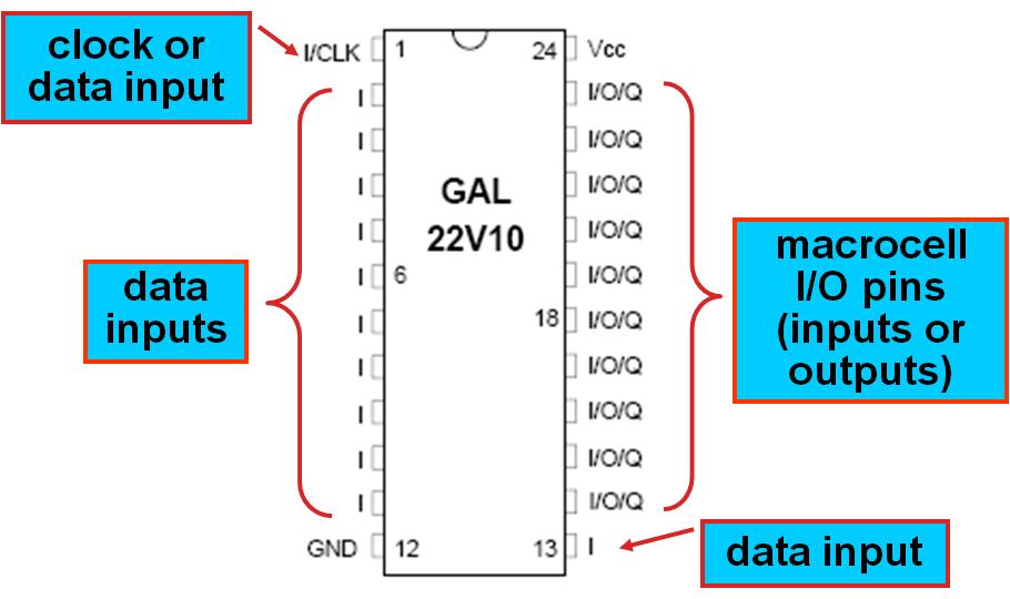
12 example GAL22V10 12
13 o complex PLDs (CPLDs) modern complex PLDs (CPLDs) contain hundreds of macrocells and I/O pins, and are designed to be erased/reprogrammed in-circuit (called isp ) because CPLDs typically contain significantly more macrocells than I/O pins, capability is provided to use macrocell resources internally (called a node) a global routing pool (GRP) is used to connect generic logic blocks (GLBs) output routing pools (ORPs) connect the GLBs to the I/O blocks (IOBs), which contain multiple I/O cells example: ispmach4000ze-series o field programmable gate arrays (FPGAs) a field programmable gate array (FPGA) is kind of like a CPLD turned insideout logic is broken into a large number of programmable blocks called look-up tables (LUTs) or configurable logic blocks (CLBs) programming configuration is stored in SRAM-based memory cells and is therefore volatile, meaning the FPGA configuration is lost when power is removed programming information must therefore be loaded into an FPGA (typically from an external ROM chip) each time it is powered up ( initialization/boot cycle) LUTs/CLBs are inherently less capable than PLD macrocells, but many more of them will fit on a comparably sized FPGA (than macrocells on a CPLD) 13
14 Lecture Summary Module 2-F Hardware Description Languages Reference: Digital Design Principles and Practices (4 th Ed.), pp overview o hardware description languages (HDLs) are the most common way to describe the programming configuration of a CPLD or an FPGA o the first HDL to enjoy widespread use was PALASM ( PAL Assembler ) from Monolithic Memories, Inc. (inventors of the PAL device) o early HDLs only supported equation entry o next generation languages such as CUPL (Compiler Universal for Programmable Logic) and ABEL (Advanced Boolean Expression Language) added more advanced capabilities: truth tables and clocked operator tables logic minimization high-level constructs such as when-else-then and state diagram test vectors timing analysis o VHDL and Verilog started out as simulation languages (later developments in these languages allowed actual hardware design) support modular, hierarchical coding and support a wide variety of high-level programming constructs represents a higher level of abstraction arrays procedures function calls conditional and iterative statements potential pitfall because VHDL and Verilog have their genesis as simulation languages, it is possible to create non-synthesizable HDL code using them (i.e., code that can simulate a digital system, but not actually realize it) concentration on use of Verilog o You will use Verilog to program legacy PLDs (like the 22V10) as well as current generation CPLDs (like the ispmach 4256ZE) o We will use the Lattice isplever Classic 1.8 software package in lab, which includes support for Verilog free copy of software package available at latticesemi.com o Verilog program contents documentation (program name, comments) declarations that identify the inputs and outputs of the logic functions to be performed statements that specify the logic functions to be performed 14
15 o Verilog program semantics identifiers (module names, signal/variables names) must begin with a letter or underscore and can include digits and dollar signs ($) identifiers are case sensitive single line comments begin with // /* comments can also be done this way */ input and output declarations tell the compiler about symbolic names associated with the external pins of the device each assign statement describes a small piece of logic circuitry Constant values can be described as n bxxxx where n is the bit-width of the signal and x is 0 or 1 o Verilog wire type wire is a basic data type in Verilog Similar to an actual wire, these variables cannot store logic value and are used to connect signals between inputs, outputs and logic elements such as gates wire is used to model Combinational Logic wire can take on four basic values 0 logical zero 1 logical one X Unknown value Z High-Impedance state o Verilog Bitwise Operators & AND OR ^ XOR ~^ or ^~ XNOR ~ NOT (similar to bitwise operators in C - you will learn about logical Verilog operators later, and the difference between the two) o isplever Operators isplever reports use different notation for some operators & AND # OR! NOT $ XOR!$ XNOR o Verilog assign statements assign statements are used to continuously assign the value of the expression on the right of the = to the signal on the left assigning constant bits to a variable assign A = 3 b110; assign B = 3 b101; assigning logic to a variable assign X = A & B; assign Y = A B; 15

16 o Verilog Module Structure synthesis loc is a compiler directive that tells isplever to use specific pins for input or output. input wire Sel, A, B /* synthesis loc= 4,5,6 */; tells compiler to connect Sel, A, and B, to pins 4, 5 and 6, respectively on the PLD o example ABEL program with equations o Verilog reg data types similar to wire, but reg can be used to store information like registers unlike wire, reg can be used to model both Combinational and Sequential logic For behavioral code using an always block, the output must be type reg For dataflow code with assign statements, the outputs must be of type wire o always block in Verilog always block lets you write "behavioral" style code, similar to C should have a sensitivity list associated with it, all statements in the always block will be evaluated when the conditions in this list are triggered conditions may be any change to the signal or rising or falling edges of the signals examples of always block: (A,B,C) begin o all statements will be evaluated whenever A, B, or C change their values (posedge CLK) begin o all statements will be evaluated on the positive (rising) edge of the CLK signal (*) begin o all statements will be evaluated whenever any input signal in the always block changes 16
.")
 and compared against values of their total bit width If the logic does not cover all possible bit combinations of the comparison")
17 o Verilog case Syntax similar to the case structure in C compares expression to a set of cases and evaluates the statement(s) associated with first matching case all cases defined between case (signal).. endcase multiple statements for a case must be enclosed in a begin and end block multiple comparison signals can be concatenated as case ({signal1, signal2 signaln}) and compared against values of their total bit width If the logic does not cover all possible bit combinations of the comparison signal(s), a default case must be added. o example ABEL program with truth table o example ABEL program with multi-input XOR 17
18 detailed example crazy grader (a.k.a. arbitrary uniformed grading hack or AUGH ) o four input variables (E, R, S, T) o five output functions (A, B, C, D, F) o stick built (using SSI parts) vs. GAL22V10 (programmed using ABEL) /* Who Wants to be a Digijock */ module gameshow(e,r,s,t,a,b,c,d,f); input wire E,R,S,T /* synthesis loc= 2,3,4,5 */; output wire A,B,C,D,F /* synthesis loc= 14,15,16,17,18 */; /* Quick and easy way in Verilog */ /* by inspection from problem statement */ assign A = (R & T) (R & ~S); assign B = (E & ~R & ~S) (~R & ~T & ~S); assign C = S & ~T; assign D = T & ~E & ~R; assign F = ~A & ~B & ~C & ~D; // or assign F = E & S & T & ~R; endmodule S S B D D E E A A A A A A B B C C C C R R R vs. 5 F T T T 1/ vs. 2/ / / / / / / / / / integrated circuits total 18

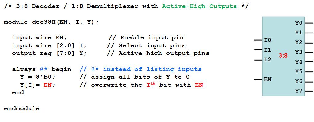
19 Lecture Summary Module 2-G Combinational Building Blocks: Decoders/Demultiplexers Reference: Digital Design Principles and Practices (4 th Ed.), pp overview o a decoder is a multiple-input, multiple-output logic circuit that converts coded inputs into coded outputs (in a one-to-one mapping, each input code word produces a different output code word) o n-bit binary input code most common o 1-out-of-m output code most common (note: output code bits are mutually exclusive) o binary decoder: n to 2 n (n-bit binary input code, 1-out-of-2 n output code) o example: 2-to-4 (2:4) binary decoder or 1-to-4 (1:4) demultiplexer Note that EN can also be construed as a digital input that is routed to the selected output, in which case the circuit would be referred to as a demultiplexer key observations o each output of an n to 2 n binary decoder represents a minterm of an n-variable Boolean function; therefore, any arbitrary Boolean function of n-variables can be realized with an n-input binary decoder by simply OR-ing the needed outputs o if the decoder outputs are active low, a NAND gate can be used to OR the minterms of the function (representing its ON set) o if the decoder outputs are active low, an AND gate can be used to OR the minterms of the complement function (representing its OFF set) o a NAND gate (or AND gate) with at most 2 n-1 inputs is needed to implement an arbitrary n-variable function using an n to 2 n binary decoder (that has active low outputs) general circuit for implementing an arbitrary n-variable function using a decoder, for case where ON set has 2 n-1 members 19
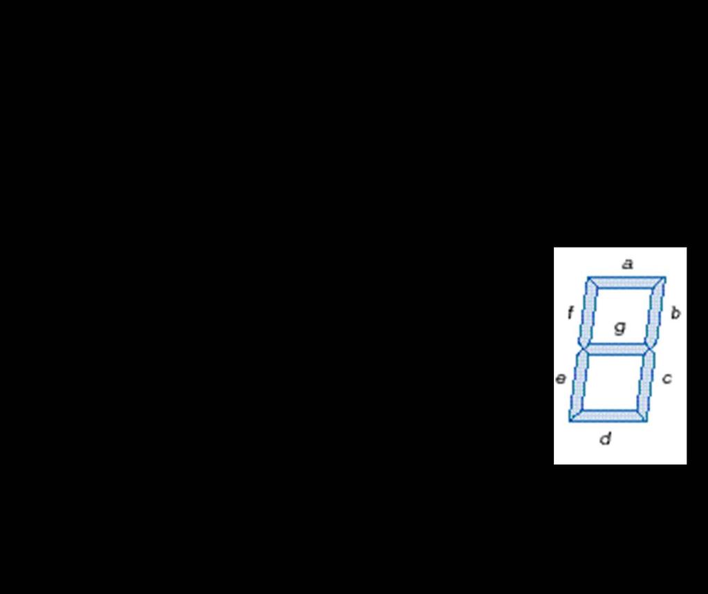
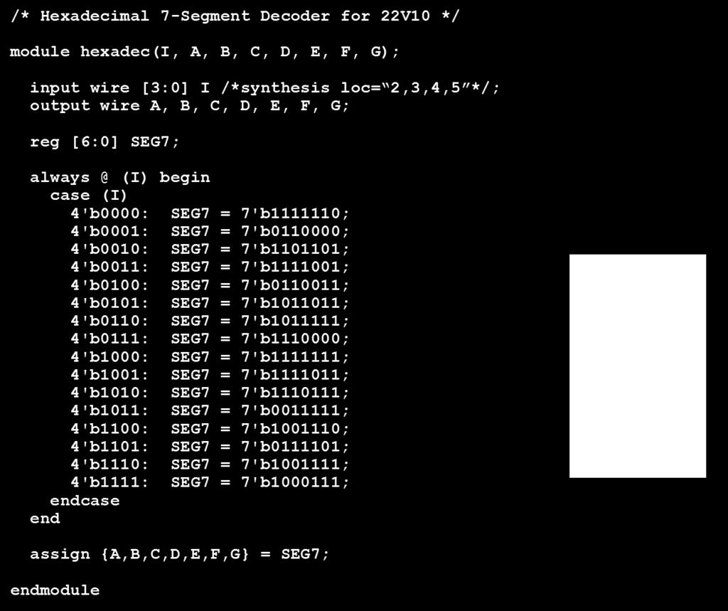
20 decoders/demultiplexers in Verilog special purpose decoders (e.g., 7-segment display) 20
21 Lecture Summary Module 2-H Combinational Building Blocks: Encoders and Tri-State Outputs Reference: Digital Design Principles and Practices (4 th Ed.), pp overview o an encoder is an inverse decoder the role of inputs and outputs is reversed, and there are more input code bits than output code bits o common application: encode device number associated with service request o problem: more than one device may be requesting service at a given instant motivation for priority encoder priority encoders o inputs are numbered, priority is assigned based on number (usually lowest number lowest priority, etc., but not always) o easiest way to do this in ABEL is with a truth table o example 8:3 priority encoder with strobe output to indicate if any of the encoder inputs have been asserted Verilog casez construct o use? as wild card o beware of non-unique expressions: 1 st matching expression wins module pri_enc(i, E, G); input wire [7:0] I; // Input 0 - lowest priority, Input 7 - highest priority output wire [2:0] E; // Encoded output output wire G; // Strobe output (asserted if any input is asserted) reg [3:0] EG; (I) begin casez (I) 8'b : EG = 4'b0000; // No inputs asserted 8'b : EG = 4'b0001; // Input 0 wins 8'b ?: EG = 4'b0011; // Input 1 wins 8'b000001??: EG = 4'b0101; // Input 2 wins 8'b00001???: EG = 4'b0111; // Input 3 wins 8'b0001????: EG = 4'b1001; // Input 4 wins 8'b001?????: EG = 4'b1011; // Input 5 wins 8'b01??????: EG = 4'b1101; // Input 6 wins 8'b1???????: EG = 4'b1111; // Input 7 wins endcase end assign {E,G} = EG; endmodule 21
22 examine the reduced equation report produced by isplever Note on isplever operators: AND - &, OR - #, NOT -!, XOR - $ Title: 8-to-3 Priority Encoder Using GAL 22V10 P-Terms Fan-in Fan-out Type Name (attributes) /1 4 1 Pin- E2 8/1 8 1 Pin- G 4/3 6 1 Pin- E1 4/4 7 1 Pin E0 ========= 20/9 Best P-Term Total: 9 Total Pins: 12 Total Nodes: 0 Average P-Term/Output: 2 Positive-Polarity (SoP) Equations: E2 = (I7 # I6 # I5 # I4); G = (I7 # I6 # I5 # I4 # I3 # I2 # I1 # I0); E1 = (I7 # I6 #!I5 &!I4 & I3 #!I5 &!I4 & I2); E0 = (I7 #!I6 & I5 #!I6 &!I4 & I3 #!I6 &!I4 &!I2 & I1); Reverse-Polarity Equations:!E2 = (!I7_&!I6_&!I5 &!I4);!G = (!I7 &!I6 &!I5 &!I4 &! 13 &!I2 &!I1 &!I0);!E1 = (!I7 &!I6 & I5 #!I7 &!I6 & I4 #!I7 &!I6 &!I3 &!I2);!E0 = (!I7 & I6 #!I7 &!I5 & I4 #!I7 &!I5 &!I3 & I2 #!I7 &!I5 &!I3 &!I1); tri-state (three-state) outputs o in Verilog, an output value of 'bz (High- Impedance or Hi-Z) assigned to an output port disables the output o tri is the datatype used for tri-state variables o can use the conditional operator "? :" to implement a tri-state buffer o example: Create a Verilog module that implements a 4:2 priority encoder with tri-state encoded outputs (E1, E0) - design should include an active high output strobe (G) that is asserted when any input is asserted module prienc42(i, E_z, G, EN); input wire [3:0] I; // Input 0 - lowest priority, // Input 3 - highest priority input wire EN; // Tri-state enable control input output tri [1:0] E_z; // Encoded tri-state enabled output output wire G; // Strobe output (high if any input is asserted) reg [2:0] EG; // EGS = {E,G} (I) begin casez (I) 4'b0000: EG = 3'b000; // No inputs active 4'b0001: EG = 3'b001; // Input 0 wins 4'b001?: EG = 3'b011; // Input 1 wins 4'b01??: EG = 3'b101; // Input 2 wins 4'b1???: EG = 3'b111; // Input 3 wins endcase end assign GS = EG[0]; assign E_z = EN? EG[2:1] : 2'bZ; endmodule 22

 1 1 a 3 D 3 Functional values assigned to each combination i 1 i 0 X Y example: 8-to-1 (8:1) multiplexer module")
23 Lecture Summary Module 2-I Combinational Building Blocks: Multiplexers Reference: Digital Design Principles and Practices (4 th Ed.), pp overview o a multiplexer is a digital switch that uses s select lines to determine which of n = 2 s inputs is connected to its output o each of the input paths may be b bits wide o equation implemented by s-select line mux is the SoP form of a general s-variable Boolen function: F(X,Y) = a0 X Y + a1 X Y + a2 X Y + a3 X Y o general structure truth table analogy X Y F(X,Y) 0 0 a a 1 D 0 D 1 Number of different functions of s variables possible: 1 0 a 2 D 2 F F(X,Y) 1 1 a 3 D 3 Functional values assigned to each combination i 1 i 0 X Y example: 8-to-1 (8:1) multiplexer module mux811(d, EN, S, Y); input wire [7:0] D; // Data inputs input wire EN; // Function enable input wire [2:0] S; // Select lines output wire Y; // Output assign Y = EN & (!S[2] &!S[1] &!S[0] & D[0]!S[2] &!S[1] & S[0] & D[1]!S[2] & S[1] &!S[0] & D[2]!S[2] & S[1] & S[0] & D[3] S[2] &!S[1] &!S[0] & D[4] S[2] &!S[1] & S[0] & D[5] S[2] & S[1] &!S[0] & D[6] S[2] & S[1] & S[0] & D[7] ); endmodule 23
![example multiplexer function realization multiplexers in ABEL (8-bit wide 4:1 mux example) module mux418a(en, S, A, B, C, D, Y_z); input wire EN; // Tri-state output enable line input wire [1:0] S;](/docs-images/76/73274602/images/24-0.jpg "// Select inputs input wire [7:0] A, B, C, D; // 8-bit input buses output tri [7:0] Y_z; // 8-bit output bus wire [7:0] Y; assign Y =!S[1] &!S[0] & A!S[1] & S[0] & B S[1] &!")
24 example multiplexer function realization multiplexers in ABEL (8-bit wide 4:1 mux example) module mux418a(en, S, A, B, C, D, Y_z); input wire EN; // Tri-state output enable line input wire [1:0] S; // Select inputs input wire [7:0] A, B, C, D; // 8-bit input buses output tri [7:0] Y_z; // 8-bit output bus wire [7:0] Y; assign Y =!S[1] &!S[0] & A!S[1] & S[0] & B S[1] &!S[0] & C S[1] & S[0] & D; assign Y_z = EN? Y : 8'bZZZZZZZZ; endmodule module mux418b(en, S, A, B, C, D, Y_z); input wire EN; // Tri-state output enable line input wire [1:0] S; // Select inputs input wire [7:0] A, B, C, D; // 8-bit input buses output tri [7:0] Y_z; // 8-bit output bus reg [7:0] Y; assign Y_z = EN? Y : 8 bzzzzzzzz; (S) begin // Y = 8 b ; if (S == 2'b00) Y = A; else if (S == 2'b01) Y = B; else if (S == 2'b10) Y = C; else if (S == 2'b11) Y = D; // else Y = 8 b ; end endmodule 24

25 Lecture Summary Module 2-J Top Level (Hierarchical) Models Reference: Digital Design Principles and Practices (4 th Ed.), pp definition: A top level module is the highest level module in a design hierarchy that instantiates other modules and connects them separating logic across multiple modules serves the advantage of reusability for modules and removing redundant logic example: If two modules use a 4-to-1 mux, create a separate module for the mux, and simply instantiate it in the other modules follows structural style of instantiation: module_name instance_name (signal_list); signals in signal_list will be connected in the order of that module s portlist this is called port mapping by order alternatively, port mapping by name can be used, which is a more error-free method here, each signal passed to the instantiated module uses the name of the signal in the module s port list to indicate where it is connected 25
Purdue IMPACT 2015 Edition by D. G. Meyer. Introduction to Digital System Design. Module 2 Combinational Logic Circuits
 Purdue IMPACT 25 Edition by D. G. Meyer Introduction to Digital System Design Module 2 Combinational Logic Circuits Glossary of Common Terms DISCRETE LOGIC a circuit constructed using small-scale integrated
CS8803: Advanced Digital Design for Embedded Hardware
 CS883: Advanced Digital Design for Embedded Hardware Lecture 2: Boolean Algebra, Gate Network, and Combinational Blocks Instructor: Sung Kyu Lim (limsk@ece.gatech.edu) Website: http://users.ece.gatech.edu/limsk/course/cs883
Chapter 3. Gate-Level Minimization. Outlines
 Chapter 3 Gate-Level Minimization Introduction The Map Method Four-Variable Map Five-Variable Map Outlines Product of Sums Simplification Don t-care Conditions NAND and NOR Implementation Other Two-Level
DIGITAL CIRCUIT LOGIC UNIT 9: MULTIPLEXERS, DECODERS, AND PROGRAMMABLE LOGIC DEVICES
 DIGITAL CIRCUIT LOGIC UNIT 9: MULTIPLEXERS, DECODERS, AND PROGRAMMABLE LOGIC DEVICES 1 Learning Objectives 1. Explain the function of a multiplexer. Implement a multiplexer using gates. 2. Explain the
Combinational Logic II
 Combinational Logic II Ranga Rodrigo July 26, 2009 1 Binary Adder-Subtractor Digital computers perform variety of information processing tasks. Among the functions encountered are the various arithmetic
ECE 270 Learning Outcome Practice Exam B. OUTCOME #2: an ability to analyze and design combinational logic circuits.
 ECE 70 Learning Outcome - - Practice Exam B OUTCOME #: an ability to analyze and design combinational logic circuits. Multiple Choice select the single most appropriate response for each question. Note
CHAPTER 9 MULTIPLEXERS, DECODERS, AND PROGRAMMABLE LOGIC DEVICES
 CHAPTER 9 MULTIPLEXERS, DECODERS, AND PROGRAMMABLE LOGIC DEVICES This chapter in the book includes: Objectives Study Guide 9.1 Introduction 9.2 Multiplexers 9.3 Three-State Buffers 9.4 Decoders and Encoders
Boolean Algebra and Logic Gates
 Boolean Algebra and Logic Gates Binary logic is used in all of today's digital computers and devices Cost of the circuits is an important factor Finding simpler and cheaper but equivalent circuits can
Combinational Logic & Circuits
 Week-I Combinational Logic & Circuits Spring' 232 - Logic Design Page Overview Binary logic operations and gates Switching algebra Algebraic Minimization Standard forms Karnaugh Map Minimization Other
FPGA Design Challenge :Techkriti 14 Digital Design using Verilog Part 1
 FPGA Design Challenge :Techkriti 14 Digital Design using Verilog Part 1 Anurag Dwivedi Digital Design : Bottom Up Approach Basic Block - Gates Digital Design : Bottom Up Approach Gates -> Flip Flops Digital
Chapter 2. Boolean Expressions:
 Chapter 2 Boolean Expressions: A Boolean expression or a function is an expression which consists of binary variables joined by the Boolean connectives AND and OR along with NOT operation. Any Boolean
Code No: 07A3EC03 Set No. 1
 Code No: 07A3EC03 Set No. 1 II B.Tech I Semester Regular Examinations, November 2008 SWITCHING THEORY AND LOGIC DESIGN ( Common to Electrical & Electronic Engineering, Electronics & Instrumentation Engineering,
VALLIAMMAI ENGINEERING COLLEGE. SRM Nagar, Kattankulathur DEPARTMENT OF ELECTRONICS AND COMMUNICATION ENGINEERING EC6302 DIGITAL ELECTRONICS
 VALLIAMMAI ENGINEERING COLLEGE SRM Nagar, Kattankulathur-603 203 DEPARTMENT OF ELECTRONICS AND COMMUNICATION ENGINEERING EC6302 DIGITAL ELECTRONICS YEAR / SEMESTER: II / III ACADEMIC YEAR: 2015-2016 (ODD
Experiment 4 Boolean Functions Implementation
 Experiment 4 Boolean Functions Implementation Introduction: Generally you will find that the basic logic functions AND, OR, NAND, NOR, and NOT are not sufficient to implement complex digital logic functions.
Code No: R Set No. 1
 Code No: R059210504 Set No. 1 II B.Tech I Semester Supplementary Examinations, February 2007 DIGITAL LOGIC DESIGN ( Common to Computer Science & Engineering, Information Technology and Computer Science
Verilog. What is Verilog? VHDL vs. Verilog. Hardware description language: Two major languages. Many EDA tools support HDL-based design
 Verilog What is Verilog? Hardware description language: Are used to describe digital system in text form Used for modeling, simulation, design Two major languages Verilog (IEEE 1364), latest version is
Chapter 3. Boolean Algebra and Digital Logic
 Chapter 3 Boolean Algebra and Digital Logic Chapter 3 Objectives Understand the relationship between Boolean logic and digital computer circuits. Learn how to design simple logic circuits. Understand how
CONTENTS CHAPTER 1: NUMBER SYSTEM. Foreword...(vii) Preface... (ix) Acknowledgement... (xi) About the Author...(xxiii)
 Preface... (ix) Acknowledgement... (xi) About the Author...(xxiii)") CONTENTS Foreword...(vii) Preface... (ix) Acknowledgement... (xi) About the Author...(xxiii) CHAPTER 1: NUMBER SYSTEM 1.1 Digital Electronics... 1 1.1.1 Introduction... 1 1.1.2 Advantages of Digital Systems...
CONTENTS Foreword...(vii) Preface... (ix) Acknowledgement... (xi) About the Author...(xxiii) CHAPTER 1: NUMBER SYSTEM 1.1 Digital Electronics... 1 1.1.1 Introduction... 1 1.1.2 Advantages of Digital Systems...
Topics. Midterm Finish Chapter 7
 Lecture 9 Topics Midterm Finish Chapter 7 ROM (review) Memory device in which permanent binary information is stored. Example: 32 x 8 ROM Five input lines (2 5 = 32) 32 outputs, each representing a memory
Gate-Level Minimization. BME208 Logic Circuits Yalçın İŞLER
 Gate-Level Minimization BME28 Logic Circuits Yalçın İŞLER islerya@yahoo.com http://me.islerya.com Complexity of Digital Circuits Directly related to the complexity of the algebraic expression we use to
(ii) Simplify and implement the following SOP function using NOR gates:
 Simplify and implement the following SOP function using NOR gates:") DHANALAKSHMI COLLEGE OF ENGINEERING DEPARTMENT OF ELECTRONICS AND COMMUNICATION ENGINEERING EE6301 DIGITAL LOGIC CIRCUITS UNIT I NUMBER SYSTEMS AND DIGITAL LOGIC FAMILIES PART A 1. How can an OR gate be
DHANALAKSHMI COLLEGE OF ENGINEERING DEPARTMENT OF ELECTRONICS AND COMMUNICATION ENGINEERING EE6301 DIGITAL LOGIC CIRCUITS UNIT I NUMBER SYSTEMS AND DIGITAL LOGIC FAMILIES PART A 1. How can an OR gate be
Gate Level Minimization Map Method
 Gate Level Minimization Map Method Complexity of hardware implementation is directly related to the complexity of the algebraic expression Truth table representation of a function is unique Algebraically
FPGA: FIELD PROGRAMMABLE GATE ARRAY Verilog: a hardware description language. Reference: [1]
![FPGA: FIELD PROGRAMMABLE GATE ARRAY Verilog: a hardware description language. Reference: [1]](/thumbs/80/81661285.jpg "FPGA: FIELD PROGRAMMABLE GATE ARRAY Verilog: a hardware description language. Reference: [1]") FPGA: FIELD PROGRAMMABLE GATE ARRAY Verilog: a hardware description language Reference: [] FIELD PROGRAMMABLE GATE ARRAY FPGA is a hardware logic device that is programmable Logic functions may be programmed
FPGA: FIELD PROGRAMMABLE GATE ARRAY Verilog: a hardware description language Reference: [] FIELD PROGRAMMABLE GATE ARRAY FPGA is a hardware logic device that is programmable Logic functions may be programmed
ECE 2300 Digital Logic & Computer Organization. More Sequential Logic Verilog
 ECE 2300 Digital Logic & Computer Organization Spring 2018 More Sequential Logic Verilog Lecture 7: 1 Announcements HW3 will be posted tonight Prelim 1 Thursday March 1, in class Coverage: Lectures 1~7
Programmable Logic Devices UNIT II DIGITAL SYSTEM DESIGN
 Programmable Logic Devices UNIT II DIGITAL SYSTEM DESIGN 2 3 4 5 6 7 8 9 2 3 4 5 6 7 8 9 2 Implementation in Sequential Logic 2 PAL Logic Implementation Design Example: BCD to Gray Code Converter A B
Boolean Algebra. BME208 Logic Circuits Yalçın İŞLER
 Boolean Algebra BME28 Logic Circuits Yalçın İŞLER islerya@yahoo.com http://me.islerya.com 5 Boolean Algebra /2 A set of elements B There exist at least two elements x, y B s. t. x y Binary operators: +
Midterm Exam Review. CS 2420 :: Fall 2016 Molly O'Neil
 Midterm Exam Review CS 2420 :: Fall 2016 Molly O'Neil Midterm Exam Thursday, October 20 In class, pencil & paper exam Closed book, closed notes, no cell phones or calculators, clean desk 20% of your final
Lecture (05) Boolean Algebra and Logic Gates
 Boolean Algebra and Logic Gates") Lecture (05) Boolean Algebra and Logic Gates By: Dr. Ahmed ElShafee ١ Minterms and Maxterms consider two binary variables x and y combined with an AND operation. Since eachv ariable may appear in either
Lecture (05) Boolean Algebra and Logic Gates By: Dr. Ahmed ElShafee ١ Minterms and Maxterms consider two binary variables x and y combined with an AND operation. Since eachv ariable may appear in either
COPYRIGHTED MATERIAL INDEX
 INDEX Absorption law, 31, 38 Acyclic graph, 35 tree, 36 Addition operators, in VHDL (VHSIC hardware description language), 192 Algebraic division, 105 AND gate, 48 49 Antisymmetric, 34 Applicable input
DHANALAKSHMI SRINIVASAN COLLEGE OF ENGINEERING AND TECHNOLOGY
 DHANALAKSHMI SRINIVASAN COLLEGE OF ENGINEERING AND TECHNOLOGY Dept/Sem: II CSE/03 DEPARTMENT OF ECE CS8351 DIGITAL PRINCIPLES AND SYSTEM DESIGN UNIT I BOOLEAN ALGEBRA AND LOGIC GATES PART A 1. How many
Contents. Appendix D Verilog Summary Page 1 of 16
 Appix D Verilog Summary Page 1 of 16 Contents Appix D Verilog Summary... 2 D.1 Basic Language Elements... 2 D.1.1 Keywords... 2 D.1.2 Comments... 2 D.1.3 Identifiers... 2 D.1.4 Numbers and Strings... 3
KING FAHD UNIVERSITY OF PETROLEUM & MINERALS COMPUTER ENGINEERING DEPARTMENT
 KING FAHD UNIVERSITY OF PETROLEUM & MINERALS COMPUTER ENGINEERING DEPARTMENT COE 202: Digital Logic Design Term 162 (Spring 2017) Instructor: Dr. Abdulaziz Barnawi Class time: U.T.R.: 11:00-11:50AM Class
Code No: R Set No. 1
 Code No: R059210504 Set No. 1 II B.Tech I Semester Regular Examinations, November 2006 DIGITAL LOGIC DESIGN ( Common to Computer Science & Engineering, Information Technology and Computer Science & Systems
Outline. EECS Components and Design Techniques for Digital Systems. Lec 11 Putting it all together Where are we now?
 Outline EECS 5 - Components and Design Techniques for Digital Systems Lec Putting it all together -5-4 David Culler Electrical Engineering and Computer Sciences University of California Berkeley Top-to-bottom
Introduction to synthesis. Logic Synthesis
 Introduction to synthesis Lecture 5 Logic Synthesis Logic synthesis operates on boolean equations and produce optimized combinational logic Logic Minimization Two-level logic minimization Two-level logic
Chapter 2 Combinational Logic Circuits
 Logic and Computer Design Fundamentals Chapter 2 Combinational Logic Circuits Part 2 Circuit Optimization Overview Part Gate Circuits and Boolean Equations Binary Logic and Gates Boolean Algebra Standard
Verilog Tutorial - Edited for CS141
 - Edited for CS141 Lukasz Strozek October 8, 2005 Based on Weste and Harris and Verilog According to Tom 1 Introduction Verilog is language commonly used in designing digital systems. It s a hardware description
SUBJECT CODE: IT T35 DIGITAL SYSTEM DESIGN YEAR / SEM : 2 / 3
 UNIT - I PART A (2 Marks) 1. Using Demorgan s theorem convert the following Boolean expression to an equivalent expression that has only OR and complement operations. Show the function can be implemented
Digital Design with FPGAs. By Neeraj Kulkarni
 Digital Design with FPGAs By Neeraj Kulkarni Some Basic Electronics Basic Elements: Gates: And, Or, Nor, Nand, Xor.. Memory elements: Flip Flops, Registers.. Techniques to design a circuit using basic
B.Tech II Year I Semester (R13) Regular Examinations December 2014 DIGITAL LOGIC DESIGN
 Regular Examinations December 2014 DIGITAL LOGIC DESIGN") B.Tech II Year I Semester () Regular Examinations December 2014 (Common to IT and CSE) (a) If 1010 2 + 10 2 = X 10, then X is ----- Write the first 9 decimal digits in base 3. (c) What is meant by don
B.Tech II Year I Semester () Regular Examinations December 2014 (Common to IT and CSE) (a) If 1010 2 + 10 2 = X 10, then X is ----- Write the first 9 decimal digits in base 3. (c) What is meant by don
Chapter 2 Basic Logic Circuits and VHDL Description
 Chapter 2 Basic Logic Circuits and VHDL Description We cannot solve our problems with the same thinking we used when we created them. ----- Albert Einstein Like a C or C++ programmer don t apply the logic.
Contents. Chapter 3 Combinational Circuits Page 1 of 34
 Chapter 3 Combinational Circuits Page of 34 Contents Contents... 3 Combinational Circuits... 2 3. Analysis of Combinational Circuits... 2 3.. Using a Truth Table... 2 3..2 Using a Boolean unction... 4
Gate-Level Minimization
 Gate-Level Minimization ( 范倫達 ), Ph. D. Department of Computer Science National Chiao Tung University Taiwan, R.O.C. Fall, 2017 ldvan@cs.nctu.edu.tw http://www.cs.nctu.edu.tw/~ldvan/ Outlines The Map Method
Incompletely Specified Functions with Don t Cares 2-Level Transformation Review Boolean Cube Karnaugh-Map Representation and Methods Examples
 Lecture B: Logic Minimization Incompletely Specified Functions with Don t Cares 2-Level Transformation Review Boolean Cube Karnaugh-Map Representation and Methods Examples Incompletely specified functions
QUESTION BANK FOR TEST
 CSCI 2121 Computer Organization and Assembly Language PRACTICE QUESTION BANK FOR TEST 1 Note: This represents a sample set. Please study all the topics from the lecture notes. Question 1. Multiple Choice
Embedded Controller Design. CompE 270 Digital Systems - 5. Objective. Application Specific Chips. User Programmable Logic. Copyright 1998 Ken Arnold 1
 CompE 270 Digital Systems - 5 Programmable Logic Ken Arnold Objective Application Specific ICs Introduce User Programmable Logic Common Architectures Programmable Array Logic Address Decoding Example Development
CSE 2021 Computer Organization. The Basics of Logic Design
 CSE 2021 Computer Organization Appendix C The Basics of Logic Design Outline Fundamental Boolean operations Deriving logic expressions from truth tables Boolean Identities Simplifying logic expressions
 www.vidyarthiplus.com Question Paper Code : 31298 B.E./B.Tech. DEGREE EXAMINATION, NOVEMBER/DECEMBER 2013. Third Semester Computer Science and Engineering CS 2202/CS 34/EC 1206 A/10144 CS 303/080230012--DIGITAL
1. Mark the correct statement(s)
") 1. Mark the correct statement(s) 1.1 A theorem in Boolean algebra: a) Can easily be proved by e.g. logic induction b) Is a logical statement that is assumed to be true, c) Can be contradicted by another
1. Mark the correct statement(s) 1.1 A theorem in Boolean algebra: a) Can easily be proved by e.g. logic induction b) Is a logical statement that is assumed to be true, c) Can be contradicted by another
CS470: Computer Architecture. AMD Quad Core
 CS470: Computer Architecture Yashwant K. Malaiya, Professor malaiya@cs.colostate.edu AMD Quad Core 1 Architecture Layers Building blocks Gates, flip-flops Functional bocks: Combinational, Sequential Instruction
EECS150, Fall 2004, Midterm 1, Prof. Culler. Problem 1 (15 points) 1.a. Circle the gate-level circuits that DO NOT implement a Boolean AND function.
 1.a. Circle the gate-level circuits that DO NOT implement a Boolean AND function.") Problem 1 (15 points) 1.a. Circle the gate-level circuits that DO NOT implement a Boolean AND function. 1.b. Show that a 2-to-1 MUX is universal (i.e. that any Boolean expression can be implemented with
Problem 1 (15 points) 1.a. Circle the gate-level circuits that DO NOT implement a Boolean AND function. 1.b. Show that a 2-to-1 MUX is universal (i.e. that any Boolean expression can be implemented with
EECS Components and Design Techniques for Digital Systems. Lec 07 PLAs and FSMs 9/ Big Idea: boolean functions <> gates.
 Review: minimum sum-of-products expression from a Karnaugh map EECS 5 - Components and Design Techniques for Digital Systems Lec 7 PLAs and FSMs 9/2- David Culler Electrical Engineering and Computer Sciences
R07
 www..com www..com SET - 1 II B. Tech I Semester Supplementary Examinations May 2013 SWITCHING THEORY AND LOGIC DESIGN (Com. to EEE, EIE, BME, ECC) Time: 3 hours Max. Marks: 80 Answer any FIVE Questions
 Get Free notes at Module-I One s Complement: Complement all the bits.i.e. makes all 1s as 0s and all 0s as 1s Two s Complement: One s complement+1 SIGNED BINARY NUMBERS Positive integers (including zero)
LSN 6 Programmable Logic Devices
 LSN 6 Programmable Logic Devices Department of Engineering Technology LSN 6 What Are PLDs? Functionless devices in base form Require programming to operate The logic function of the device is programmed
CHAPTER - 2 : DESIGN OF ARITHMETIC CIRCUITS
 Contents i SYLLABUS osmania university UNIT - I CHAPTER - 1 : BASIC VERILOG HDL Introduction to HDLs, Overview of Digital Design With Verilog HDL, Basic Concepts, Data Types, System Tasks and Compiler
Computer Aided Design Basic Syntax Gate Level Modeling Behavioral Modeling. Verilog
 Verilog Radek Pelánek and Šimon Řeřucha Contents 1 Computer Aided Design 2 Basic Syntax 3 Gate Level Modeling 4 Behavioral Modeling Computer Aided Design Hardware Description Languages (HDL) Verilog C
R10. II B. Tech I Semester, Supplementary Examinations, May
 SET - 1 1. a) Convert the following decimal numbers into an equivalent binary numbers. i) 53.625 ii) 4097.188 iii) 167 iv) 0.4475 b) Add the following numbers using 2 s complement method. i) -48 and +31
Follow-up question: now, comment on what each of these acronyms actually means, going beyond a mere recitation of the definition.
 Question 1 Define the following acronyms as they apply to digital logic circuits: ASIC PAL PLA PLD CPLD FPGA file 03041 Answer 1 ASIC: Application-Specific Integrated Circuit PAL: Programmable Array Logic
structure syntax different levels of abstraction
 This and the next lectures are about Verilog HDL, which, together with another language VHDL, are the most popular hardware languages used in industry. Verilog is only a tool; this course is about digital
Here is a list of lecture objectives. They are provided for you to reflect on what you are supposed to learn, rather than an introduction to this
 This and the next lectures are about Verilog HDL, which, together with another language VHDL, are the most popular hardware languages used in industry. Verilog is only a tool; this course is about digital
ENGIN 241 Digital Systems with Lab
 ENGIN 241 Digital Systems with Lab (4) Dr. Honggang Zhang Engineering Department University of Massachusetts Boston 1 Introduction Hardware description language (HDL): Specifies logic function only Computer-aided
Programmable logic technology
 Programmable logic technology This worksheet and all related files are licensed under the Creative Commons Attribution License, version 1.0. To view a copy of this license, visit http://creativecommons.org/licenses/by/1.0/,
Optimized Implementation of Logic Functions
 June 25, 22 9:7 vra235_ch4 Sheet number Page number 49 black chapter 4 Optimized Implementation of Logic Functions 4. Nc3xe4, Nb8 d7 49 June 25, 22 9:7 vra235_ch4 Sheet number 2 Page number 5 black 5 CHAPTER
Lecture 12 VHDL Synthesis
 CPE 487: Digital System Design Spring 2018 Lecture 12 VHDL Synthesis Bryan Ackland Department of Electrical and Computer Engineering Stevens Institute of Technology Hoboken, NJ 07030 1 What is Synthesis?
Review. EECS Components and Design Techniques for Digital Systems. Lec 05 Boolean Logic 9/4-04. Seq. Circuit Behavior. Outline.
 Review EECS 150 - Components and Design Techniques for Digital Systems Lec 05 Boolean Logic 94-04 David Culler Electrical Engineering and Computer Sciences University of California, Berkeley Design flow
Verilog Design Principles
 16 h7fex // 16-bit value, low order 4 bits unknown 8 bxx001100 // 8-bit value, most significant 2 bits unknown. 8 hzz // 8-bit value, all bits high impedance. Verilog Design Principles ECGR2181 Extra Notes
Simplification of Boolean Functions
 COM111 Introduction to Computer Engineering (Fall 2006-2007) NOTES 5 -- page 1 of 5 Introduction Simplification of Boolean Functions You already know one method for simplifying Boolean expressions: Boolean
Digital Design Using Digilent FPGA Boards -- Verilog / Active-HDL Edition
 Digital Design Using Digilent FPGA Boards -- Verilog / Active-HDL Edition Table of Contents 1. Introduction to Digital Logic 1 1.1 Background 1 1.2 Digital Logic 5 1.3 Verilog 8 2. Basic Logic Gates 9
IE1204 Digital Design L7: Combinational circuits, Introduction to VHDL
 IE24 Digital Design L7: Combinational circuits, Introduction to VHDL Elena Dubrova KTH / ICT / ES dubrova@kth.se This lecture BV 38-339, 6-65, 28-29,34-365 IE24 Digital Design, HT 24 2 The multiplexer
END-TERM EXAMINATION
 (Please Write your Exam Roll No. immediately) END-TERM EXAMINATION DECEMBER 2006 Exam. Roll No... Exam Series code: 100919DEC06200963 Paper Code: MCA-103 Subject: Digital Electronics Time: 3 Hours Maximum
EE 8351 Digital Logic Circuits Ms.J.Jayaudhaya, ASP/EEE
 EE 8351 Digital Logic Circuits Ms.J.Jayaudhaya, ASP/EEE 1 Logic circuits for digital systems may be combinational or sequential. A combinational circuit consists of input variables, logic gates, and output
CS211 Digital Systems/Lab. Introduction to VHDL. Hyotaek Shim, Computer Architecture Laboratory
 CS211 Digital Systems/Lab Introduction to VHDL Hyotaek Shim, Computer Architecture Laboratory Programmable Logic Device (PLD) 2/32 An electronic component used to build reconfigurable digital circuits
HDLs and SystemVerilog. Digital Computer Design
 HDLs and SystemVerilog Digital Computer Design Logic Arrays Gates can be organized into regular arrays. If the connections are made programmable, these logic arrays can be configured to perform any function
ECE 331 Digital System Design
 ECE 331 Digital System Design Tristate Buffers, Read-Only Memories and Programmable Logic Devices (Lecture #17) The slides included herein were taken from the materials accompanying Fundamentals of Logic
Chapter 2. Boolean Algebra and Logic Gates
 Chapter 2. Boolean Algebra and Logic Gates Tong In Oh 1 Basic Definitions 2 3 2.3 Axiomatic Definition of Boolean Algebra Boolean algebra: Algebraic structure defined by a set of elements, B, together
UNIT- V COMBINATIONAL LOGIC DESIGN
 UNIT- V COMBINATIONAL LOGIC DESIGN NOTE: This is UNIT-V in JNTUK and UNIT-III and HALF PART OF UNIT-IV in JNTUA SYLLABUS (JNTUK)UNIT-V: Combinational Logic Design: Adders & Subtractors, Ripple Adder, Look
Memory and Programmable Logic
 Memory and Programmable Logic Memory units allow us to store and/or retrieve information Essentially look-up tables Good for storing data, not for function implementation Programmable logic device (PLD),
PALs, GALs & CUPL. What is Programmable Logic?
 PALs, GALs & CUPL A lesson on Programmable Logic Devices and programming them using CUPL What is Programmable Logic? Digital integrated circuits where the Boolean function can be determined by the user.
CSE140L: Components and Design Techniques for Digital Systems Lab
 CSE140L: Components and Design Techniques for Digital Systems Lab Tajana Simunic Rosing Source: Vahid, Katz, Culler 1 Announcements & Outline Lab 4 due; demo signup times listed on the cse140l site Check
ECE 545 Lecture 5. Data Flow Modeling in VHDL. George Mason University
 ECE 545 Lecture 5 Data Flow Modeling in VHDL George Mason University Required reading P. Chu, RTL Hardware Design using VHDL Chapter 4, Concurrent Signal Assignment Statements of VHDL 2 Types of VHDL Description
Design of Digital Circuits Lecture 6: Combinational Logic, Hardware Description Lang. & Verilog. Prof. Onur Mutlu ETH Zurich Spring March 2018
 Design of Digital Circuits Lecture 6: Combinational Logic, Hardware Description Lang. & Verilog Prof. Onur Mutlu ETH Zurich Spring 2018 9 March 2018 Required Lecture Video Why study computer architecture?
Synthesis of Combinational and Sequential Circuits with Verilog
 Synthesis of Combinational and Sequential Circuits with Verilog What is Verilog? Hardware description language: Are used to describe digital system in text form Used for modeling, simulation, design Two
EEL 4783: HDL in Digital System Design
 EEL 4783: HDL in Digital System Design Lecture 15: Logic Synthesis with Verilog Prof. Mingjie Lin 1 Verilog Synthesis Synthesis vs. Compilation Descriptions mapped to hardware Verilog design patterns for
Chapter 13 Programmable Logic Device Architectures
 Chapter 13 Programmable Logic Device Architectures Chapter 13 Objectives Selected areas covered in this chapter: Describing different categories of digital system devices. Describing different types of
Chapter 2: Combinational Systems
 Uchechukwu Ofoegbu Chapter 2: Combinational Systems Temple University Adapted from Alan Marcovitz s Introduction to Logic and Computer Design Riddle Four switches can be turned on or off. One is the switch
COMBINATIONAL LOGIC CIRCUITS
 COMBINATIONAL LOGIC CIRCUITS 4.1 INTRODUCTION The digital system consists of two types of circuits, namely: (i) Combinational circuits and (ii) Sequential circuits A combinational circuit consists of logic
Chapter 3 Part 2 Combinational Logic Design
 University of Wisconsin - Madison ECE/Comp Sci 352 Digital Systems Fundamentals Kewal K. Saluja and Yu Hen Hu Spring 2002 Chapter 3 Part 2 Combinational Logic Design Originals by: Charles R. Kime and Tom
Gate-Level Minimization. section instructor: Ufuk Çelikcan
 Gate-Level Minimization section instructor: Ufuk Çelikcan Compleity of Digital Circuits Directly related to the compleity of the algebraic epression we use to build the circuit. Truth table may lead to
CSE140L: Components and Design
 CSE140L: Components and Design Techniques for Digital Systems Lab Tajana Simunic Rosing Source: Vahid, Katz, Culler 1 Grade distribution: 70% Labs 35% Lab 4 30% Lab 3 20% Lab 2 15% Lab 1 30% Final exam
Last Name Student Number. Last Name Student Number
 University of Toronto Faculty of Applied Science and Engineering Department of Electrical and Computer Engineering Midterm Examination ECE 241F - Digital Systems Wednesday October 13, 2004, 6:00pm [5]
Experiment 3: Logic Simplification
 Module: Logic Design Name:... University no:.. Group no:. Lab Partner Name: Mr. Mohamed El-Saied Experiment : Logic Simplification Objective: How to implement and verify the operation of the logical functions
Chapter 3 working with combinational logic
 hapter 3 working with combinational logic ombinational Logic opyright 24, Gaetano orriello and Randy H. Katz Working with combinational logic Simplification two-level simplification exploiting don t cares
DIGITAL CIRCUIT LOGIC UNIT 7: MULTI-LEVEL GATE CIRCUITS NAND AND NOR GATES
 DIGITAL CIRCUIT LOGIC UNIT 7: MULTI-LEVEL GATE CIRCUITS NAND AND NOR GATES 1 iclicker Question 13 Considering the K-Map, f can be simplified as (2 minutes): A) f = b c + a b c B) f = ab d + a b d AB CD
COLLEGE OF ENGINEERING DEPARTMENT OF ELECTRICAL AND ELECTRONICS ENGINEERING QUESTION BANK SUBJECT CODE & NAME: EC 1312 DIGITAL LOGIC CIRCUITS UNIT I
 KINGS COLLEGE OF ENGINEERING DEPARTMENT OF ELECTRICAL AND ELECTRONICS ENGINEERING QUESTION BANK SUBJECT CODE & NAME: EC 1312 DIGITAL LOGIC CIRCUITS YEAR / SEM: III / V UNIT I NUMBER SYSTEM & BOOLEAN ALGEBRA
SHRI ANGALAMMAN COLLEGE OF ENGINEERING. (An ISO 9001:2008 Certified Institution) SIRUGANOOR, TIRUCHIRAPPALLI
 SIRUGANOOR, TIRUCHIRAPPALLI") SHRI ANGALAMMAN COLLEGE OF ENGINEERING AND TECHNOLOGY (An ISO 9001:2008 Certified Institution) SIRUGANOOR, TIRUCHIRAPPALLI 621 105 DEPARTMENT OF ELECTRONICS AND COMMUNICATION ENGINEERING EC1201 DIGITAL
SHRI ANGALAMMAN COLLEGE OF ENGINEERING AND TECHNOLOGY (An ISO 9001:2008 Certified Institution) SIRUGANOOR, TIRUCHIRAPPALLI 621 105 DEPARTMENT OF ELECTRONICS AND COMMUNICATION ENGINEERING EC1201 DIGITAL
VALLIAMMAI ENGINEERING COLLEGE
 VALLIAMMAI ENGINEERING COLLEGE SRM Nagar, Kattankulathur 603 203 DEPARTMENT OF INFORMATION TECHNOLOGY & COMPUTER SCIENCE AND ENGINEERING QUESTION BANK II SEMESTER CS6201- DIGITAL PRINCIPLE AND SYSTEM DESIGN
Verilog Module 1 Introduction and Combinational Logic
 Verilog Module 1 Introduction and Combinational Logic Jim Duckworth ECE Department, WPI 1 Module 1 Verilog background 1983: Gateway Design Automation released Verilog HDL Verilog and simulator 1985: Verilog
Verilog Fundamentals. Shubham Singh. Junior Undergrad. Electrical Engineering
 Verilog Fundamentals Shubham Singh Junior Undergrad. Electrical Engineering VERILOG FUNDAMENTALS HDLs HISTORY HOW FPGA & VERILOG ARE RELATED CODING IN VERILOG HDLs HISTORY HDL HARDWARE DESCRIPTION LANGUAGE
Summary. Boolean Addition
 Summary Boolean Addition In Boolean algebra, a variable is a symbol used to represent an action, a condition, or data. A single variable can only have a value of or 0. The complement represents the inverse