Part B. Dengxue Yan Washington University in St. Louis
|
|
|
- Norah Simpson
- 5 years ago
- Views:
Transcription
1 Tools Tutorials Part B Dengxue Yan Washington University in St. Louis
2 Tools mainly used in this class Synopsys VCS Simulation Synopsys Design Compiler Generate gate-level netlist Cadence Encounter placing and routing
3 Outline Synopsys Design Compiler Cadence Encounter
4 Design Compiler Introduction We use Synopsys Design Compiler (DC) to synthesize Verilog RTL models into a gatelevel netlist where all of the gates are from the standard cell library. So Synopsys DC will synthesize the Verilog + operator into a specific arithmetic block at the gate-level. Based on various constraints it may synthesize a ripple-carry adder, a carry-look-ahead adder, or even more advanced parallel-prefix adders.

5 Design Compiler TCL File
6 Design Compiler TCL File Setup library set search_path set symbol_lib "vtvt_tsmc180.sdb"
7 Design Compiler TCL File Constraint setting set_input_delay Sets input delay on pins or input ports relative to a clock signal. set_max_area Specifies the maximum area for the current design. set_max_delay Specifies a maximum delay target for selected paths in the current design. set_min_delay Specifies a minimum delay target for selected paths in the current design.
8 Design Compiler TCL File Design Compiler settings check_design check_timing report_area report_timing_requirements
9 Design Compiler TCL File Report files define redirect [format "%s%s" $my_toplevel _design.repc] { report_design } redirect [format "%s%s" $my_toplevel _area.repc] { report_area }
10 Design Compiler TCL File Other command Look at the Design Compiler User Guide on blackboard for detail.
11 Design Compiler Compile Compile the files by typing in the terminal: % dc_shell-t -f <file>.tcl In the above example, it should be: % dc_shell-t -f compiledc.tcl After run this command, there might be some warning but no error presented in the terminal. Otherwise you need to check your code or tcl file and correct them according to the related messages.
12 Design Compiler Timing Report <my_toplevel>_min_timing.repc <my_toplevel>_max_timing.repc <my_toplevel>_out_min_timing.repc Make sure the timing report requirements are MET. You can observe which module in the design is giving the maximum delay and optimize accordingly.

13 Design Compiler

14 Design Compiler Power Report <my_toplevel>_power.repc
15 Design Compiler Area Report <my_toplevel>_area.repc
16 Outline Synopsys Design Compiler Cadence Encounter
17 Cadence Encounter Introduction We use Cadence Encounter for placing and routing standard cells, but also for power routing and clock tree synthesis. The Verilog gate-level netlist generated by Synopsys DC has no physical information: it is just a netlist, so the Cadence Encounter will first try and do a rough placement of all of the gates into rows on the chip. Cadence Encounter will then do some preliminary routing, and iterate between more and more detailed placement and routing until it reaches the target cycle time (or gives up). Cadence Encounter will also route all of the power and ground rails in a grid and connect this grid to the power and ground pins of each standard cell, and Cadence Encounter will automatically generate a clock tree to distribute the clock to all sequential state elements with hopefully low skew. The automated flow for place-and-route is much more sophisticated compared to what we did in the previous tutorial.

18 Encounter View File This is a file generated by Design Compiler. (You need to change it according to your design)

19 Encounter Start Encounter

20 Encounter Import Design

21 Encounter Floor Plan

22 Encounter Power Route Setting

23 Encounter Pins Editting

24 Encounter Place standard cell
25 Encounter Clock tree synthesis Download Clock.ctstch and place it in working directory. Download Clock.tcl and place it in working directory. Open Clock.tcl using gedit and copy the content line by line to the encounter terminal and execute it.
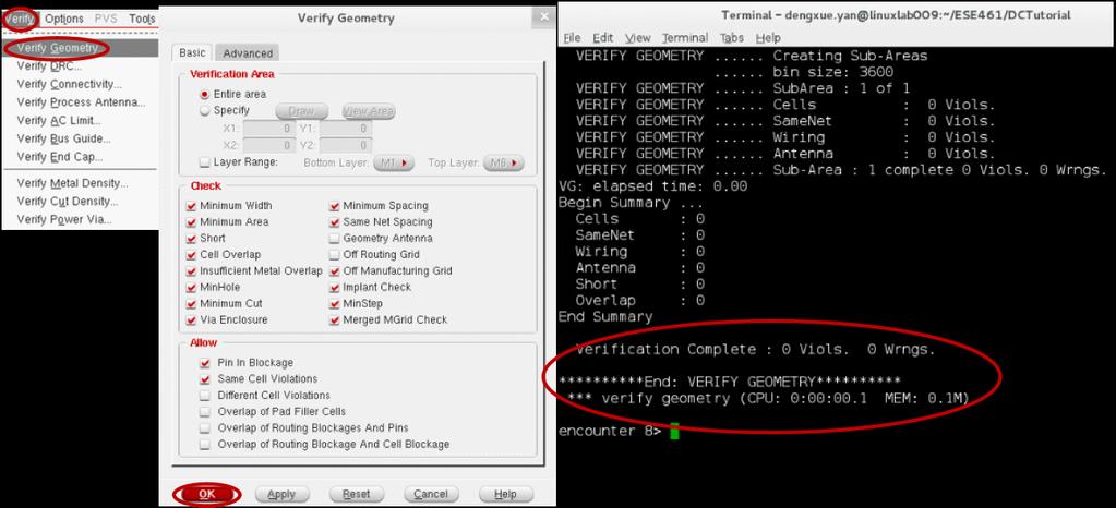
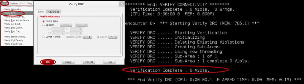
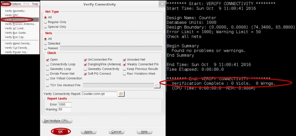
26 Encounter Verification
27 Encounter

28 Encounter

29 Encounter
30 Acknowledgement
Getting a Quick Start 2
 2 Getting a Quick Start 2 This chapter walks you through the basic synthesis design flow (shown in Figure 2-1). You use the same basic flow for both design exploration and design implementation. The following
Overview. Design flow. Principles of logic synthesis. Logic Synthesis with the common tools. Conclusions
 Logic Synthesis Overview Design flow Principles of logic synthesis Logic Synthesis with the common tools Conclusions 2 System Design Flow Electronic System Level (ESL) flow System C TLM, Verification,
Logic Synthesis. Logic Synthesis. Gate-Level Optimization. Logic Synthesis Flow. Logic Synthesis. = Translation+ Optimization+ Mapping
 Logic Synthesis Logic Synthesis = Translation+ Optimization+ Mapping Logic Synthesis 2 Gate-Level Optimization Logic Synthesis Flow 3 4 Design Compiler Procedure Logic Synthesis Input/Output 5 6 Design
Tutorial for Encounter
 Tutorial for Encounter STEP 1: Login to the Linux system on Linuxlab server. Start a terminal (the shell prompt). (If you don t know how to login to Linuxlab server, look at here) Click here to open a
Lecture 11 Logic Synthesis, Part 2
 Lecture 11 Logic Synthesis, Part 2 Xuan Silvia Zhang Washington University in St. Louis http://classes.engineering.wustl.edu/ese461/ Write Synthesizable Code Use meaningful names for signals and variables
Tutorial 2.(b) : Synthesizing your design using the Synopsys Design Compiler ( For DFT Flow)
 : Synthesizing your design using the Synopsys Design Compiler ( For DFT Flow)") Tutorial 2.(b) : Synthesizing your design using the Synopsys Design Compiler ( For DFT Flow) Objectives: In this tutorial you will learrn to use Synopsys Design Compiler (DC) to perform hardware synthesis
Tutorial 2.(b) : Synthesizing your design using the Synopsys Design Compiler ( For DFT Flow) Objectives: In this tutorial you will learrn to use Synopsys Design Compiler (DC) to perform hardware synthesis
Tutorial for Cadence SOC Encounter Place & Route
 Tutorial for Cadence SOC Encounter Place & Route For Encounter RTL-to-GDSII System 13.15 T. Manikas, Southern Methodist University, 3/9/15 Contents 1 Preliminary Setup... 1 1.1 Helpful Hints... 1 2 Starting
Laboratory 6. - Using Encounter for Automatic Place and Route. By Mulong Li, 2013
 CME 342 (VLSI Circuit Design) Laboratory 6 - Using Encounter for Automatic Place and Route By Mulong Li, 2013 Reference: Digital VLSI Chip Design with Cadence and Synopsys CAD Tools, Erik Brunvand Background
Synthesis and APR Tools Tutorial
 Synthesis and APR Tools Tutorial (Last updated: Oct. 26, 2008) Introduction This tutorial will get you familiarized with the design flow of synthesizing and place and routing a Verilog module. All the
Tutorial for Verilog Synthesis Lab (Part 2)
") Tutorial for Verilog Synthesis Lab (Part 2) Before you synthesize your code, you must absolutely make sure that your verilog code is working properly. You will waste your time if you synthesize a wrong
Tutorial for Verilog Synthesis Lab (Part 2) Before you synthesize your code, you must absolutely make sure that your verilog code is working properly. You will waste your time if you synthesize a wrong
The IIT standard cell library Version 2.1
 The IIT standard cell library Version 2.1 Highlights - Support for AMI 0.35um library, including pads - Added Primetime and Pathmill support to IIT ASIC Flow - Support for stacked vias (for Virtuoso and
An overview of standard cell based digital VLSI design
 An overview of standard cell based digital VLSI design Implementation of the first generation AsAP processor Zhiyi Yu and Tinoosh Mohsenin VCL Laboratory UC Davis Outline Overview of standard cellbased
TOPIC : Verilog Synthesis examples. Module 4.3 : Verilog synthesis
 TOPIC : Verilog Synthesis examples Module 4.3 : Verilog synthesis Example : 4-bit magnitude comptarator Discuss synthesis of a 4-bit magnitude comparator to understand each step in the synthesis flow.
Cell-Based Design Flow. TA : 吳廸優
 Cell-Based Design Flow TA : 吳廸優 dywu@viplab.cs.nctu.edu.tw 1 Outline Overview Design Flow Stage 1 RTL Development Synthesis Gate Level Simulation Design Flow Stage 2 Placement and Routing Post Layout Simulation
Physical Placement with Cadence SoCEncounter 7.1
 Physical Placement with Cadence SoCEncounter 7.1 Joachim Rodrigues Department of Electrical and Information Technology Lund University Lund, Sweden November 2008 Address for correspondence: Joachim Rodrigues
CAD for VLSI Design - I. Lecture 21 V. Kamakoti and Shankar Balachandran
 CAD for VLSI Design - I Lecture 21 V. Kamakoti and Shankar Balachandran Overview of this Lecture Understanding the process of Logic synthesis Logic Synthesis of HDL constructs Logic Synthesis What is this?
Automated Synthesis from HDL models. Design Compiler (Synopsys) Leonardo (Mentor Graphics)
 Leonardo (Mentor Graphics)") Automated Synthesis from HDL models Design Compiler (Synopsys) Leonardo (Mentor Graphics) Front-End Design & Verification VHDL Verilog SystemC Create Behavioral/RTL HDL Model(s) VHDL-AMS Verilog-A ModelSim
Automated Synthesis from HDL models Design Compiler (Synopsys) Leonardo (Mentor Graphics) Front-End Design & Verification VHDL Verilog SystemC Create Behavioral/RTL HDL Model(s) VHDL-AMS Verilog-A ModelSim
A. Setting Up the Environment a. ~/ece394 % mkdir synopsys b.
 ECE 394 ASIC & FPGA Design Synopsys Design Compiler and Design Analyzer Tutorial A. Setting Up the Environment a. Create a new folder (i.e. synopsys) under your ece394 directory ~/ece394 % mkdir synopsys
Laboratory 5. - Using Design Compiler for Synthesis. By Mulong Li, 2013
 CME 342 (VLSI Circuit Design) Laboratory 5 - Using Design Compiler for Synthesis By Mulong Li, 2013 Reference: http://www.tkt.cs.tut.fi/tools/public/tutorials/synopsys/design_compiler/gsdc.html Background
EE 330 Laboratory Experiment Number 11 Design, Simulation and Layout of Digital Circuits using Hardware Description Languages
 EE 330 Laboratory Experiment Number 11 Design, Simulation and Layout of Digital Circuits using Hardware Description Languages Purpose: The purpose of this experiment is to develop methods for using Hardware
EE 330 Laboratory Experiment Number 11
 EE 330 Laboratory Experiment Number 11 Design and Simulation of Digital Circuits using Hardware Description Languages Fall 2017 Contents Purpose:... 3 Background... 3 Part 1: Inverter... 4 1.1 Simulating
Hardware Verification Group. Department of Electrical and Computer Engineering, Concordia University, Montreal, Canada. CAD Tool Tutorial.
 Digital Logic Synthesis and Equivalence Checking Tools Hardware Verification Group Department of Electrical and Computer Engineering, Concordia University, Montreal, Canada CAD Tool Tutorial May, 2010
Outline. SoC Encounter Flow. Typical Backend Design Flow. Digital IC-Project and Verification. Place and Route. Backend ASIC Design flow
 Outline Digital IC-Project and Verification Deepak Dasalukunte Backend ASIC Design flow General steps Input files Floorplanning Placement Clock-synthesis Routing Typical Backend Design Flow SoC Encounter
DESIGN STRATEGIES & TOOLS UTILIZED
 CHAPTER 7 DESIGN STRATEGIES & TOOLS UTILIZED 7-1. Field Programmable Gate Array The internal architecture of an FPGA consist of several uncommitted logic blocks in which the design is to be encoded. The
King Fahd University of Petroleum and Minerals. Computer Engineering Department. COE 561 Digital Systems Design and Synthesis (Course Activity)
") King Fahd University of Petroleum and Minerals Computer Engineering Department COE 561 Digital Systems Design and Synthesis (Course Activity) Synthesis using Synopsys Design Compiler Tutorial The Synthesis
King Fahd University of Petroleum and Minerals Computer Engineering Department COE 561 Digital Systems Design and Synthesis (Course Activity) Synthesis using Synopsys Design Compiler Tutorial The Synthesis
CPE/EE 427, CPE 527, VLSI Design I: Tutorial #4, Standard cell design flow (from verilog to layout, 8-bit accumulator)
") CPE/EE 427, CPE 527, VLSI Design I: Tutorial #4, Standard cell design flow (from verilog to layout, 8-bit accumulator) Joel Wilder, Aleksandar Milenkovic, ECE Dept., The University of Alabama in Huntsville
CPE/EE 427, CPE 527, VLSI Design I: Tutorial #4, Standard cell design flow (from verilog to layout, 8-bit accumulator) Joel Wilder, Aleksandar Milenkovic, ECE Dept., The University of Alabama in Huntsville
Graduate Institute of Electronics Engineering, NTU Synopsys Synthesis Overview
 Synopsys Synthesis Overview Ben 2006.02.16 ACCESS IC LAB Outline Introduction Setting Design Environment Setting Design Constraints Synthesis Report and Analysis pp. 2 What is Synthesis Synthesis = translation
Introduction to Design Compiler
 Introduction to Design Compiler Courtesy of Dr. An-Yeu Wu @NTU, CIC/NARL@Taiwan http://csce.uark.edu +1 (479) 575-6043 yrpeng@uark.edu What is Synthesis Synthesis = translation + optimization We will get
Hardware Design Environments. Dr. Mahdi Abbasi Computer Engineering Department Bu-Ali Sina University
 Hardware Design Environments Dr. Mahdi Abbasi Computer Engineering Department Bu-Ali Sina University Outline Welcome to COE 405 Digital System Design Design Domains and Levels of Abstractions Synthesis
DC-Tcl Procedures. Learning Objectives. After completing this lab, you should be able to: Write generic DC-Tcl procedures. Lab Duration: 30 minutes
 w 14 Learning Objectives After completing this lab, you should be able to: Write generic DC-Tcl procedures Lab Duration: 30 minutes Lab 14-1 Synopsys 31833-000-S38 Flow Diagram of Lab Create and test myprocs.tcl
MOJTABA MAHDAVI Mojtaba Mahdavi DSP Design Course, EIT Department, Lund University, Sweden
 High Level Synthesis with Catapult MOJTABA MAHDAVI 1 Outline High Level Synthesis HLS Design Flow in Catapult Data Types Project Creation Design Setup Data Flow Analysis Resource Allocation Scheduling
CS/EE 6710 Digital VLSI Design Tutorial on Cadence to Synopsys Interface (CSI)
") CS/EE 6710 Digital VLSI Design Tutorial on Cadence to Synopsys Interface (CSI) This tutorial walks you through the Cadence to Synopsys Interface (CSI). This interface lets you take a schematic from composer
CS/EE 6710 Digital VLSI Design Tutorial on Cadence to Synopsys Interface (CSI) This tutorial walks you through the Cadence to Synopsys Interface (CSI). This interface lets you take a schematic from composer
Multiple Clocks and Timing Exceptions
 10 Multiple Clocks and Timing Exceptions Learning Objectives This lab is intended to give you a better understanding of how static timing analysis works and how timing exceptions are properly applied.
RTL Coding General Concepts
 RTL Coding General Concepts Typical Digital System 2 Components of a Digital System Printed circuit board (PCB) Embedded d software microprocessor microcontroller digital signal processor (DSP) ASIC Programmable
ECE 5745 ASIC Tutorial
 README.md - Grip ECE 5745 ASIC Tutorial This tutorial will explain how to use a set of Synopsys tools to push an RTL design through synthesis, place-and-route, and power analysis. This tutorial assumes
Bits and Pieces of CS250 s Toolflow
 Bits and Pieces of CS250 s Toolflow CS250 Tutorial 2 (Version 092509a) September 25, 2009 Yunsup Lee In this tutorial you will learn what each VLSI tools used in class are meant to do, how they flow, file
RTL Synthesis using Design Compiler. Dr Basel Halak
 RTL Synthesis using Design Compiler Dr Basel Halak Learning Outcomes: After completing this unit, you should be able to: 1. Set up the DC RTL Synthesis Software and run synthesis tasks 2. Synthesize a
18. Synopsys Formality Support
 18. Synopsys Formality Support QII53015-7.2.0 Introduction Formal verification of FPGA designs is gaining momentum as multi-million System-on-a-Chip (SoC) designs are targeted at FPGAs. Use the Formality
An Overview of Standard Cell Based Digital VLSI Design
 An Overview of Standard Cell Based Digital VLSI Design With examples taken from the implementation of the 36-core AsAP1 chip and the 1000-core KiloCore chip Zhiyi Yu, Tinoosh Mohsenin, Aaron Stillmaker,
University of California, Davis Department of Electrical and Computer Engineering. EEC180B DIGITAL SYSTEMS Spring Quarter 2018
 University of California, Davis Department of Electrical and Computer Engineering EEC180B DIGITAL SYSTEMS Spring Quarter 2018 LAB 2: FPGA Synthesis and Combinational Logic Design Objective: This lab covers
Bits and Pieces of CS250 s Toolflow
 Bits and Pieces of CS250 s Toolflow CS250 Tutorial 2 (Version 091210a) September 12, 2010 Yunsup Lee In this tutorial you will learn what each VLSI tools used in class are meant to do, how they flow, file
CMOS VLSI Design Lab 3: Controller Design and Verification
 CMOS VLSI Design Lab 3: Controller Design and Verification The controller for your MIPS processor is responsible for generating the signals to the datapath to fetch and execute each instruction. It lacks
FPGA Design Flow 1. All About FPGA
 FPGA Design Flow 1 In this part of tutorial we are going to have a short intro on FPGA design flow. A simplified version of FPGA design flow is given in the flowing diagram. FPGA Design Flow 2 FPGA_Design_FLOW
HDL Compiler Directives 7
 7 HDL Compiler Directives 7 Directives are a special case of regular comments and are ignored by the Verilog HDL simulator HDL Compiler directives begin, like all other Verilog comments, with the characters
Hardware Verification Group
 Digital Logic Synthesis and Equivalence Checking Tools Tutorial Hardware Verification Group Department of Electrical and Computer Engineering, Concordia University, Montreal, Canada {n ab, h aridh}@encs.concordia.ca
EE 4755 Digital Design Using Hardware Description Languages
 EE 4755 Digital Design Using Hardware Description Languages Basic Information URL: http://www.ece.lsu.edu/v Offered by: David M. Koppelman, Room 345 ERAD Building 578-5482. koppel@ece.lsu.edu, http://www.ece.lsu.edu/koppel/koppel.html
CMOS VLSI Design Lab 3: Controller Design and Verification
 CMOS VLSI Design Lab 3: Controller Design and Verification The controller for your MIPS processor is responsible for generating the signals to the datapath to fetch and execute each instruction. It lacks
Chapter 2 Getting Hands on Altera Quartus II Software
 Chapter 2 Getting Hands on Altera Quartus II Software Contents 2.1 Installation of Software... 20 2.2 Setting Up of License... 21 2.3 Creation of First Embedded System Project... 22 2.4 Project Building
Cell-Based Design Flow. 林丞蔚
 Cell-Based Design Flow 林丞蔚 cultom@viplab.cs.nctu.edu.tw 1 Outline Overview Design Flow 1 RTL Development Synthesis Gate Level Simulation Design Flow 2 Placement and Routing Example Design IC Contest 2006
Don t expect to be able to write and debug your code during the lab session.
 EECS150 Spring 2002 Lab 4 Verilog Simulation Mapping UNIVERSITY OF CALIFORNIA AT BERKELEY COLLEGE OF ENGINEERING DEPARTMENT OF ELECTRICAL ENGINEERING AND COMPUTER SCIENCE Lab 4 Verilog Simulation Mapping
Compile RISC_CORE. Learning Objectives. After completing this lab, you should be able to: Perform a top-down compile strategy on the RISC_CORE design
 15 Learning Objectives After completing this lab, you should be able to: Perform a top-down compile strategy on the RISC_CORE design Lab Duration: 75 minutes Lab 15-1 Synopsys 31833-000-S38 Flow Diagram
Setup file.synopsys_dc.setup
 Setup file.synopsys_dc.setup The.synopsys_dc.setup file is the setup file for Synopsys' Design Compiler. Setup file is used for initializing design parameters and variables, declare design libraries, and
EE 466/586 VLSI Design. Partha Pande School of EECS Washington State University
 EE 466/586 VLSI Design Partha Pande School of EECS Washington State University pande@eecs.wsu.edu Lecture 18 Implementation Methods The Design Productivity Challenge Logic Transistors per Chip (K) 10,000,000.10m
Design Tools for 100,000 Gate Programmable Logic Devices
 esign Tools for 100,000 Gate Programmable Logic evices March 1996, ver. 1 Product Information Bulletin 22 Introduction The capacity of programmable logic devices (PLs) has risen dramatically to meet the
CMOS VLSI Design Lab 3: Controller Design and Verification
 CMOS VLSI Design Lab 3: Controller Design and Verification The controller for your MIPS processor is responsible for generating the signals to the datapath to fetch and execute each instruction. It lacks
EE 330 Laboratory Experiment Number 11 Design and Simulation of Digital Circuits using Hardware Description Languages
 EE 330 Laboratory Experiment Number 11 Design and Simulation of Digital Circuits using Hardware Description Languages Fall 2015 Purpose: The purpose of this experiment is to develop methods for using Hardware
ESE 570 Cadence Lab Assignment 2: Introduction to Spectre, Manual Layout Drawing and Post Layout Simulation (PLS)
") ESE 570 Cadence Lab Assignment 2: Introduction to Spectre, Manual Layout Drawing and Post Layout Simulation (PLS) Objective Part A: To become acquainted with Spectre (or HSpice) by simulating an inverter,
ESE 570 Cadence Lab Assignment 2: Introduction to Spectre, Manual Layout Drawing and Post Layout Simulation (PLS) Objective Part A: To become acquainted with Spectre (or HSpice) by simulating an inverter,
Partitioning for Better Synthesis Results
 3 Partitioning for Better Synthesis Results Learning Objectives After completing this lab, you should be able to: Use the group and ungroup commands to repartition a design within Design Analyzer Analyze
Synopsys ASIC Tutorial
 Synopsys ASIC Tutorial Version 11.0 Updated November 30, 2015 Linux log in and tutorial Synthesis with dc_shell Timing Area Chip implementaeon with icc_shell Placement RouEng Clock tree Finishing Chip
Lab 3 Verilog Simulation Mapping
 University of California at Berkeley College of Engineering Department of Electrical Engineering and Computer Sciences 1. Motivation Lab 3 Verilog Simulation Mapping In this lab you will learn how to use
PG Certificate. VLSI Design & Verification (RTL using Verilog, FPGA Design Flow & Verification) (Live Project)
 (Live Project)") PG Certificate in VLSI Design & Verification (RTL using Verilog, FPGA Design Flow & Verification) (Live Project) Certificates by National Skill Development Corporation (NSDC), Ministry of Skill Development
PG Certificate in VLSI Design & Verification (RTL using Verilog, FPGA Design Flow & Verification) (Live Project) Certificates by National Skill Development Corporation (NSDC), Ministry of Skill Development
CSE P567 - Winter 2010 Lab 1 Introduction to FGPA CAD Tools
 CSE P567 - Winter 2010 Lab 1 Introduction to FGPA CAD Tools This is a tutorial introduction to the process of designing circuits using a set of modern design tools. While the tools we will be using (Altera
Digital IC- Project 1. Place and Route. Oskar Andersson. Oskar Andersson, EIT, LTH, Digital IC project and Verifica=on
 Digital IC- Project 1 Oskar Andersson Outline Backend ASIC Design flow (Physical Design) General steps Input files Floorplanning Placement ClockTree- synthesis Rou=ng Typical Backend Design Flow Synthesis
Circuit Design and Simulation with VHDL 2nd edition Volnei A. Pedroni MIT Press, 2010 Book web:
 Circuit Design and Simulation with VHDL 2nd edition Volnei A. Pedroni MIT Press, 2010 Book web: www.vhdl.us Appendix C Xilinx ISE Tutorial (ISE 11.1) This tutorial is based on ISE 11.1 WebPack (free at
CPE/EE 427, CPE 527, VLSI Design I: Tutorial #3, Standard cell design flow (from schematic to layout, 8-bit accumulator)
") CPE/EE 427, CPE 527, VLSI Design I: Tutorial #3, Standard cell design flow (from schematic to layout, 8-bit accumulator) Joel Wilder, Aleksandar Milenkovic, ECE Dept., The University of Alabama in Huntsville
CPE/EE 427, CPE 527, VLSI Design I: Tutorial #3, Standard cell design flow (from schematic to layout, 8-bit accumulator) Joel Wilder, Aleksandar Milenkovic, ECE Dept., The University of Alabama in Huntsville
CPE 200L LABORATORY 4: INTRODUCTION TO DE2 BOARD UNIVERSITY OF NEVADA, LAS VEGAS GOALS: BACKGROUND:
 CPE 200L LABORATORY 4: INTRODUCTION TO DE2 BOARD DEPARTMENT OF ELECTRICAL AND COMPUTER ENGINEERING UNIVERSITY OF NEVADA, LAS VEGAS GOALS: Getting familiar with DE2 board installation, properties, usage.
11. Synopsys Design Compiler FPGA Support
 11. Synopsys Design Compiler FPGA Support QII51014-7.2.0 Introduction Programmable logic device (PLD) designs have reached the complexity and performance requirements of ASIC designs. As a result, advanced
Concurrent, OA-based Mixed-signal Implementation
 Concurrent, OA-based Mixed-signal Implementation Mladen Nizic Eng. Director, Mixed-signal Solution 2011, Cadence Design Systems, Inc. All rights reserved worldwide. Mixed-Signal Design Challenges Traditional
Creating Verilog Tutorial Netlist Release Date: 01/13/2005(Version 2)
") Creating Verilog Tutorial 2-1 - Creating a verilog netlist for a schematic: The verilog netlist is necessary for automatic layout (placement and routing) tools. It contains information about the I/O pins
Creating Verilog Tutorial 2-1 - Creating a verilog netlist for a schematic: The verilog netlist is necessary for automatic layout (placement and routing) tools. It contains information about the I/O pins
Lab. Course Goals. Topics. What is VLSI design? What is an integrated circuit? VLSI Design Cycle. VLSI Design Automation
 Course Goals Lab Understand key components in VLSI designs Become familiar with design tools (Cadence) Understand design flows Understand behavioral, structural, and physical specifications Be able to
Digital Systems Laboratory
 2012 Fall CSE140L Digital Systems Laboratory by Dr. Choon Kim CSE Department UCSD 1 Welcome to CSE140L! 2 3-way Light Controller, 2-1 MUX, Majority Detector, 7- seg Display, Binary-to- Decimal converter.
8. Best Practices for Incremental Compilation Partitions and Floorplan Assignments
 8. Best Practices for Incremental Compilation Partitions and Floorplan Assignments QII51017-9.0.0 Introduction The Quartus II incremental compilation feature allows you to partition a design, compile partitions
PrimeTime: Introduction to Static Timing Analysis Workshop
 i-1 PrimeTime: Introduction to Static Timing Analysis Workshop Synopsys Customer Education Services 2002 Synopsys, Inc. All Rights Reserved PrimeTime: Introduction to Static 34000-000-S16 Timing Analysis
EECS 627, Lab Assignment 2
 EECS 627, Lab Assignment 2 1 Introduction In this lab assignment, you will extend the process of designing your multiplier chip. You will add two more blocks (a pseudo-random test pattern generator and
From Concept to Silicon
 From Concept to Silicon How an idea becomes a part of a new chip at ATI Richard Huddy ATI Research From Concept to Silicon Creating a new Visual Processing Unit (VPU) is a complex task involving many people
EE 4755 Digital Design Using Hardware Description Languages
 EE 4755 Digital Design Using Hardware Description Languages Basic Information URL: http://www.ece.lsu.edu/v Offered by: David M. Koppelman, Room 3316R P. F. Taylor Hall 578-5482. koppel@ece.lsu.edu, http://www.ece.lsu.edu/koppel/koppel.html
and 32 bit for 32 bit. If you don t pay attention to this, there will be unexpected behavior in the ISE software and thing may not work properly!
 This tutorial will show you how to: Part I: Set up a new project in ISE 14.7 Part II: Implement a function using Schematics Part III: Simulate the schematic circuit using ISim Part IV: Constraint, Synthesize,
Synthesizable FPGA Fabrics Targetable by the VTR CAD Tool
 Synthesizable FPGA Fabrics Targetable by the VTR CAD Tool Jin Hee Kim and Jason Anderson FPL 2015 London, UK September 3, 2015 2 Motivation for Synthesizable FPGA Trend towards ASIC design flow Design
Verilog Simulation Mapping
 1 Motivation UNIVERSITY OF CALIFORNIA AT BERKELEY COLLEGE OF ENGINEERING DEPARTMENT OF ELECTRICAL ENGINEERING AND COMPUTER SCIENCE Lab 4 Verilog Simulation Mapping In this lab you will learn how to use
AccelDSP tutorial 2 (Matlab.m to HDL for Xilinx) Ronak Gandhi Syracuse University Fall
 Ronak Gandhi Syracuse University Fall") AccelDSP tutorial 2 (Matlab.m to HDL for Xilinx) Ronak Gandhi Syracuse University Fall 2009-10 AccelDSP Getting Started Tutorial Introduction This tutorial exercise will guide you through the process of
AccelDSP tutorial 2 (Matlab.m to HDL for Xilinx) Ronak Gandhi Syracuse University Fall 2009-10 AccelDSP Getting Started Tutorial Introduction This tutorial exercise will guide you through the process of
An introduction to CoCentric
 A Hand-Out 1 An introduction to CoCentric Las Palmas de G. C., Spain Jun, 27 th, 2002 Agenda 2 System-level SoC design What is SystemC? CoCentric System Studio SystemC based designs verification CoCentric
Cell-Based IC Physical Design & Verification SOC Encounter. Advisor : 李昆忠 Presenter : 蕭智元
 Cell-Based IC Physical Design & Verification SOC Encounter Advisor : 李昆忠 Presenter : 蕭智元 Reference: SOC Encounter Training Manual, 2007, edited by CIC. Introduction We ll use some EDA tools to transform
Pipelined MIPS CPU Synthesis and On-Die Representation ECE472 Joseph Crop Stewart Myers
 Pipelined MIPS CPU Synthesis and On-Die Representation ECE472 Joseph Crop Stewart Myers 2008 Table of Contents Introduction... 3 Steps Taken and Simulation... 3 Pitfalls... 8 Simulated Delay... 9 APPENDIX
Logic synthesis and Place and Route Tutorial Page 1
 Logic synthesis and Place and Route Tutorial Page 1 Standard Cell ASIC Design flow: A designer uses predesigned logic cells such as AND gate, NOR gate, etc. These gates are called Standard Cells. The advantage
Tutorial 2 Automatic Placement & Routing
 Tutorial 2 Automatic Placement & Routing Please follow the instructions found under Setup on the CADTA main page before starting this tutorial. 1.1. Start Encounter Log on to a VLSI server using your EE
Digital Design LU. Lab Exercise 1
 Digital Design LU Lab Exercise 1 Jakob Lechner, Thomas Polzer {lechner, tpolzer}@ecs.tuwien.ac.at Department of Computer Engineering University of Technology Vienna Vienna, October 4, 2010 1 Overview 1
Actel Libero TM Integrated Design Environment v2.3 Structural Schematic Flow Design Tutorial
 Actel Libero TM Integrated Design Environment v2.3 Structural Schematic Flow Design Tutorial 1 Table of Contents Design Flow in Libero TM IDE v2.3 Step 1 - Design Creation 3 Step 2 - Design Verification
Graphics: Alexandra Nolte, Gesine Marwedel, Universität Dortmund. RTL Synthesis
 Graphics: Alexandra Nolte, Gesine Marwedel, 2003 Universität Dortmund RTL Synthesis Purpose of HDLs Purpose of Hardware Description Languages: Capture design in Register Transfer Language form i.e. All
EEL 5722C Field-Programmable Gate Array Design
 EEL 5722C Field-Programmable Gate Array Design Lecture 17: Describing Synthesizable RTL in SystemC* Prof. Mingjie Lin * 2001 Synopsys, Inc. 1 System-Level Design Specifying the system Verifying its functionality
ECE 459/559 Secure & Trustworthy Computer Hardware Design
 ECE 459/559 Secure & Trustworthy Computer Hardware Design VLSI Design Basics Garrett S. Rose Spring 2016 Recap Brief overview of VHDL Behavioral VHDL Structural VHDL Simple examples with VHDL Some VHDL
SmartTime for Libero SoC v11.5
 SmartTime for Libero SoC v11.5 User s Guide NOTE: PDF files are intended to be viewed on the printed page; links and cross-references in this PDF file may point to external files and generate an error
EEM216A Design of VLSI Circuits and Systems Fall To start physical synthesis, you will need to source and launch IC Compiler.
 EEM216A Design of VLSI Circuits and Systems Fall 2012 Prof. Dejan Marković IC Compiler Tutorial Launching IC Compiler To start physical synthesis, you will need to source and launch IC Compiler. tcsh source
Evolution of CAD Tools & Verilog HDL Definition
 Evolution of CAD Tools & Verilog HDL Definition K.Sivasankaran Assistant Professor (Senior) VLSI Division School of Electronics Engineering VIT University Outline Evolution of CAD Different CAD Tools for
Synopsys ASIC Tutorial
 Synopsys ASIC Tutorial Version 11.4 Updated December 14th, 2015 Linux log in and tutorial Synthesis with dc_shell Timing Area Chip implementaeon with icc_shell Placement RouEng Clock tree Finishing Verify
Synthesis. Other key files. Standard cell (NAND, NOR, Flip-Flop, etc.) FPGA CLB
 FPGA CLB") SYNTHESIS Synthesis Involves synthesizing a gate netlist from verilog source code We use Design Compiler (DC) by Synopsys which is the most popular synthesis tool used in industry Target library examples:
SYNTHESIS Synthesis Involves synthesizing a gate netlist from verilog source code We use Design Compiler (DC) by Synopsys which is the most popular synthesis tool used in industry Target library examples:
Top-down digital design flow
 6 Dec 2005 Top-down digital design flow EDA tools: Modelsim, Synopsys Design Compiler, Cadence Encounter Alain Vachoux Microelectronic Systems Lab STI-IMM-LSM alain.vachoux@epfl.ch version 3.0.2 / 6 Dec
1 Design Process HOME CONTENTS INDEX. For further assistance, or call your local support center
 1 Design Process VHDL Compiler, a member of the Synopsys HDL Compiler family, translates and optimizes a VHDL description to an internal gate-level equivalent. This representation is then compiled with
Digital Design with FPGAs. By Neeraj Kulkarni
 Digital Design with FPGAs By Neeraj Kulkarni Some Basic Electronics Basic Elements: Gates: And, Or, Nor, Nand, Xor.. Memory elements: Flip Flops, Registers.. Techniques to design a circuit using basic
VHDL introduction Notes
 UH Hawaii Manoa 475 Electronics for physicists VHDL introduction Notes Author: Andrej Seljak Date: Fall 2016 update 1 Ver: 1.0 Table of Contents 1. FPGA description3 2. USB EVALUATION board 4 3. ISE Xilinx
ENEE245 Digital Circuits and Systems Lab Manual
 ENEE245 Digital Circuits and Systems Lab Manual Department of Engineering, Physical & Computer Sciences Montgomery College Version 1.1 Copyright Prof. Lan Xiang (Do not distribute without permission) 1