SWITCHING THEORY AND LOGIC CIRCUITS
|
|
|
- Brett Campbell
- 5 years ago
- Views:
Transcription
1 SWITCHING THEORY AND LOGIC CIRCUITS
2 COURSE OBJECTIVES. To understand the concepts and techniques associated with the number systems and codes 2. To understand the simplification methods (Boolean algebra & postulates, k-map method and tabular method) to simplify the given Boolean function. 3. To understand the fundamentals of digital logic and to design various combinational and sequential circuits. 4. To understand the concepts of programmable logic devices(plds) 5. To understand formal procedure for the analysis and design of synchronous and asynchronous sequential logic
3 COURSE OUTCOMES After completion of the course the student will be able to. Understand the concepts and techniques of number systems and codes in representing numerical values in various number systems and perform number conversions between different number systems and codes. 2. Apply the simplification methods to simplify the given Boolean function (Boolean algebra, k-map and Tabular method). 3. Implement given Boolean function using logic gates, MSI circuits and/ or PLD s.
4 COURSE OUTCOMES After completion of the course the student will be able to 4. Design and decoders, analyze encoders, various combinational multiplexers, and circuits like de-multiplexers, arithmetic circuits (half adder, full adder, multiplier etc). 5. Design and analyze various sequential circuits like flip-flops, registers, counters etc. 6. Analyze and Design synchronous and asynchronous sequential circuits.
5 UNIT-I Introductory Concepts (Number systems, Base conversions)
6 Digital Systems Digital systems consider discrete amounts of data Examples 26 letters in the alphabet decimal digits Larger quantities can be built from discrete values: Words made of letters Numbers made of decimal digits (e.g ) Computers operate on binary values ( and ) Easy to represent binary values electrically Voltages and currents Can be implemented using circuits Create the building blocks of modern computers
7 Understanding Decimal Numbers Decimal numbers are made of decimal digits: (,,2,3,4,5,6,7,8,9) Base = How many items does decimal number 8653 represents? 8653 Weight = 8 x3 + 6 x2 + 5 x + 3 x Number = d3 x B3 + d2 x B2 + d x B + d x B = Value What about fractions? = 9x4 + 7x3 + 6x2 + 5x + 4x + 3x- + 5x-2 In formal notation ( )
8 Understanding Octal Numbers Octal numbers are made of octal digits: (,,2,3,4,5,6,7) How many items does an octal number represent? = Weights (4536)8 = 4x83 + 5x82 + 3x8 + 6x8 = (2398) What about fractions? (465.27)8 = 4x82 + 6x8 + 5x8 + 2x8- + 7x8-2 Octal numbers don t use digits 8 or 9
9 Understanding Hexadecimal Numbers Hexadecimal numbers are made of 6 digits: (,,2,3,4,5,6,7,8,9,A, B, C, D, E, F) How many items does a hex number represent? = Weights (3A9F)6 = 3x63 + x62 + 9x6 + 5x6 = 4999 What about fractions? (2D3.5)6 = 2x62 + 3x6 + 3x6 + 5x6- = Note that each hexadecimal digit can be represented with four bits ()2 = (E)6 Groups of four bits are called a nibble ()2
10 Understanding Binary Numbers Binary numbers are made of binary digits (bits): and How many items does a binary number represent? = Weights ()2 = x23 + x22 + x2 + x2 = () What about fractions? (.)2 = x22 + x2 + x2 + x2- + x2-2 Groups of eight bits are called a byte ()2 Groups of four bits are called a nibble ()2

11 Putting It All Together Binary, octal, and hexadecimal are similar Easy to build circuits to operate on these representations Possible to convert between the three formats

12 Why Use Binary Numbers? Easy to represent and using electrical values Possible to tolerate noise Easy to transmit data Easy to build binary circuits AND Gate
13 Conversion Between Number Bases Learn to convert between bases Already demonstrated how to convert from binary to decimal Octal (base 8) Decimal (base ) Binary (base 2) Hexadecimal (base 6)
14 Convert an Integer from Decimal to Another Base For each digit position:. Divide decimal number by the base (e.g. 2) 2. The remainder is the lowest-order digit 3. Repeat first two steps until no divisor remains Example for (3): Quotient Remainder 3/2 = 6/2 = 3/2 = /2 = Coefficient a = a = a2 = a3 = Answer (3) = (a3 a2 a a)2 = ()2 MSB LSB
15 Convert a Fraction from Decimal to Another Base For each digit position:. Multiply decimal number by the base (e.g. 2) 2. The integer is the highest-order digit 3. Repeat first two steps until fraction becomes zero Example for (.625): Integer.625 x 2 =.25 x 2 =.5 x 2 = Fraction Coefficient a- = a-2 = a-3 = Answer (.625) = (.a- a-2 a-3 )2 = (.)2 MSB LSB
16 The Growth of Binary Numbers n 2n n 2n 2= 8 28=256 2=2 9 29= =4 2= =8 2= =6 2 22= = =M Mega 6 26= =G Giga 7 27= =T Tera Kilo
17 Convert an Integer from Decimal to Octal For each digit position:. Divide decimal number by the base (8) 2. The remainder is the lowest-order digit 3. Repeat first two steps until no divisor remains Example for (75): Quotient 75/8 = 2/8 = 2/8 = Remainder Coefficient a = 7 a = 5 a2 = 2 Answer (75) = (a2 a a)8 = (257)8
18 Convert a Fraction from Decimal to Octal For each digit position:. Multiply decimal number by the base (e.g. 8) 2. The integer is the highest-order digit 3. Repeat first two steps until fraction becomes zero Example for (.325): Fraction Integer.325 x 8 =.5 x 8 = Coefficient.5. Answer (.325) = (.24)8 a- = 2 a-2 = 4
19 Conversion Between Base 6 and Base 2 Conversion is easy! Determine the 4-bit binary value for each hex digit Note that there are 6 different values of four bits Easier to read and write in hexadecimal Representations are equivalent! 3A9F6 = 2 3 A 9 F
20 Conversion Between Base 6 and Base 8. Convert from Base 6 to Base 2 2. Regroup bits into groups of three starting from right 3. Ignore leading zeros 4. Each group of three bits forms an octal digit 3A9F6 = = A 9 F
21 Binary Addition Binary addition is very simple carries = 6 = 23 = 84
22 Binary Subtraction We can also perform subtraction (with borrows in place of carries) Let s subtract ()2 from ()2 borrows = 77 = = 54
23 Binary Multiplication Binary multiplication is much the same as decimal multiplication, except that the multiplication operations are much simpler X
24 Summary Binary numbers are made of binary digits (bits) Binary and octal number systems Conversion between number systems Addition, subtraction, and multiplication in binary
25 Introductory Concepts (Complements)
26 How To Represent Signed Numbers Plus and minus signs are used for decimal numbers: 25 (or +25), 6, etc In computers, everything is represented as bits Three types of signed binary number representations: signed magnitude s complement 2 s complement In each case: left-most bit indicates the sign: for positive and for negative
27 Signed Magnitude Representation The left most bit is designated as the sign bit while the remaining bits form the magnitude The sign bit should not be included in addition / subtraction operations 2 = 2 Sign bit Magnitude 2 = 2 Sign bit Magnitude
28 One s Complement Representation The one s complement of a binary number is done by complementing (i.e. inverting) all bits s comp of is s comp of is For a n-bit number N the s complement is (2n ) N Called diminished radix complement by Mano To find the negative of a s complement number take its s complement 2 = 2 Sign bit Magnitude 2 = 2 Sign bit Code
29 One s Complement Representation 7 4 bits 6 6 combinations
30 Two s Complement Representation The two s complement of a binary number is done by complementing (inverting) all bits then adding 2 s comp of is 2 s comp of is For an n-bit number N the 2 s complement is (2n ) N + Called radix complement by Mano To find the negative of a 2 s complement number take its 2 s complement 2 = 2 Sign bit Magnitude 2 = 2 Sign bit Code
![Two s Complement Shortcuts Algorithm : Complement each bit then add to the result N = [N] = + + Algorithm 2: Starting with](/docs-images/84/91182504/images/31-1.jpg "the least significant bit, copy all of the bits up to and including the first bit, then complement the remaining bits N [N]")
31 Two s Complement Shortcuts Algorithm : Complement each bit then add to the result N = [N] = + + Algorithm 2: Starting with the least significant bit, copy all of the bits up to and including the first bit, then complement the remaining bits N [N] = =
32 Two s Complement Representation 7 4 bits 6 6 combinations
33 Finite-Precision Number Representation Machines that use 2 s complement arithmetic can represent integers in the range 2n- N 2n- n is the number of bits used for representing N Note that 2n- = (..)2 and 2n- = (..)2 2 s complement code has more negative numbers than positive s complement code has 2 representations for zero For a n-bit number in base (i.e. radix) z there are zn different unsigned values (combinations) (,, zn-)
34 s Complement Subtraction Using s complement representation, subtracting numbers is also easy Step : Take s complement of 2nd operand Step 2: Add binary numbers Step 3: Add carry as a low order bit - For example: (+2) () s comp (+2) = +()2 + = 2 Add ( ) = ()2 Add carry = 2 in s comp Final Result
35 2 s Complement Subtraction Using 2 s complement representation, subtracting numbers is also easy Step : Take 2 s complement of 2nd operand Step 2: Add binary numbers Step 3: Ignore the resulting carry bit For example: (+2) () (+2) = +()2 = 2 ( ) = ()2 = 2 in 2 s comp. - 2 s comp + Add Final Result Ignore Carry
36 2 s Complement Subtraction Example 2: (3) (5) (3) = +()2 = ()2 ( 5) = ()2 = ()2 Adding these two 5-bit codes: + Carry Discarding the carry bit, the sign bit is seen to be zero, indicating a positive result Indeed: ()2 = +(8)
37 2 s Complement Subtraction Example 3: (5) (2) (5) = +()2 = ()2 ( 2) = ()2 = ()2 Adding these two 5-bit codes: + Carry Here, there is no carry bit and the sign bit is. This indicates a negative result, which is what we expect: ()2 = (7)
38 Summary Binary numbers can also be represented in octal and hexadecimal Easy to convert between binary, octal, and hexadecimal Signed numbers are represented in 3 codes: signed magnitude, s complement, or 2 s complement 2 s complement code is most important (only representation for zero) Important to understand the treatment of the sign bit for s and 2 s complement codes
39 Introductory Concepts (Codes)
40 Binary Coded Decimal Binary Coded Decimal (BCD) represents each decimal digit with four bits Ex. = This is NOT the same as 2 Why do this? Because people think in decimal Digit BCD Code Digit BCD Code
 Used to encode numbers for seven-segment displays Easier to")
41 Putting It All Together BCD is not very efficient Used in early computers (94s, 95s) Used to encode numbers for seven-segment displays Easier to read?
42 Binary Gray Code Only one bit changes from one decimal digit to the next 6 7 Useful for reducing errors in communication Digit Gray Code Gray code is not a number system It is an alternate way to represent four bit data Can be scaled to larger numbers
43 ASCII Code American Standard Code for Information Interchange ASCII is a 7-bit code, frequently used with a 8th bit for error detection (more about that later) Character ASCII (bin) ASCII (hex) Decimal Octal A 4 65 B C Z a
44 ASCII Codes and Data Transmission ASCII Codes A Z (26 codes), a z (26 codes) 9 ( codes), others (@#$%^&*.) Transmission susceptible to noise Typical transmission rates (5 Kbps, 56.6 Kbps) How to keep data transmission accurate?
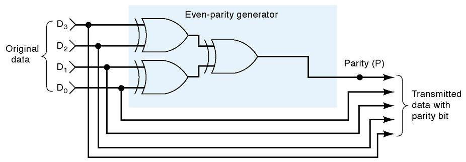
45 Parity Codes Parity codes are formed by concatenating a parity bit, P to each code word C In an even-parity code, the parity bit is specified so that the total number of ones is even In an odd-parity code, the parity bit is specified so that the total number of ones is odd P Information Bits Added even parity bit Added odd parity bit
46 Parity Code Example Concatenate a parity bit to the ASCII code for the characters, X, and = to produce both oddparity and even-parity codes Character ASCII Odd-Parity ASCII Even-Parity ASCII X =
47 Binary Data Storage Binary cells store individual bits of data Multiple cells form a register Data in registers can indicate different values Hex (binary) BCD ASCII Binary Cell
48 Register Transfer Data can move from a register to a register Digital logic used to process data Register A Register B Digital Logic Circuits Register C
49 Transfer of Information Data input at keyboard Shifted into place Stored in memory NOTE: Data input in ASCII
50 Building a Computer We need processing We need storage We need communication You will learn to use and design these components
51 Summary Although 2 s complement is most important, other number codes exist ASCII code is used to represent characters (such as those on the keyboard) Registers store binary data
52 Unit-II Boolean Algebra and Logic gates
53 Digital Systems Analysis problem: Inputs.. Logic Circuit.. Outputs Determine the binary output for each input combination Design problem: given a task, develop a circuit that accomplishes that task Many possible implementations Best circuit: based on some criterion (size, power, performance, etc.)
54 Toll Booth Controller Consider the design of a toll booth controller Inputs: quarter, car sensor Outputs: gate-lift signal, gate-close signal $.25 Car? Logic Circuit Raise gate Close gate If driver pitches in quarter, raise gate When car has cleared gate, close gate
55 Describing Circuit Functionality: Inverter Basic logic functions have symbols The same functionality can be represented with a truth table Truth table completely specifies outputs for all input combinations This is an inverter Truth Table An input of is inverted to a A Y An input of is inverted to a A Y Symbol Input Output
56 The AND Gate This is an AND gate Truth Table If the two input signals A B Y are asserted (i.e. high) the output will also be asserted. Otherwise, the output will be deasserted (i.e. low) A B Y A B
57 The OR Gate This is an OR gate If either of the two input signals is asserted, or both of them are, the output A B Y will be asserted A A B Y B
58 Describing Circuit Functionality: Waveforms Waveforms provide another approach for representing functionality Values are either high (logic ) or low (logic ) Can you create a truth table from the waveforms? AND Gate x y f
59 Consider three-input gates 3 Input OR Gate
60 Ordering Boolean Functions How to interpret A B + C? Is it A B ORed with C? Is it A ANDed with B + C? Order of precedence for Boolean algebra: AND before OR Note that parentheses are needed here:
61 Boolean Algebra A Boolean algebra is defined as a closed algebraic system containing a set K of two or more elements and the two operators, and + Useful for identifying and minimizing circuit functionality Identity elements a+=a a =a is the identity element for the + operation is the identity element for the operation
62 Commutativity and Associativity of the Operators Commutative Property: For every a and b in K, a+b=b+a a b=b a Associative Property: For every a, b, and c in K, a + (b + c) = (a + b) + c a (b c) = (a b) c
63 Distributivity of the Operators and Complements Distributive Property: For every a, b, and c in K, a+(b c)=(a+b) (a+c) a (b+c)=(a b)+(a c) The Existence of the Complement: For every a in K there exists a unique element called a (or ā) (complement of a) such that, a + a = a a = To simplify notation, the operator is frequently omitted. When two elements are written next to each other, the AND ( ) operator is implied a+b c=(a+b) (a+c) a + bc = ( a + b )( a + c )
64 Duality The principle of duality is an important concept: If an expression is valid in Boolean algebra, the dual of that expression is also valid To form the dual of an expression, replace all + operators with operators, all operators with + operators, all ones with zeros, and all zeros with ones Form the dual of the equation: a + (bc) = (a + b)(a + c) Following the replacement rules: a(b + c) = ab + ac Take care not to alter the location of the parentheses if they are present
65 Involution This theorem states: a = a a=a Remember that: aa = aa= a+a = a+a= Therefore, a is the complement of a and a is also the complement of a Taking the double inverse of a value produces the initial value
66 Absorption This theorem states: a + ab = a a(a+b) = a To prove the first half of this theorem: a + ab = a + ab = a ( + b) = a (b + ) = a () a + ab = a
67 DeMorgan s Theorem A key theorem in simplifying Boolean algebra expressions is DeMorgan s Theorem. It states: (a + b) = a b (ab) = a + b a+b =a b a b =a +b Example: Complement and simplify the expression a(b + z(x + a )) a (b + z ( x + a )) = a + (b + z (x + a )) = a + b (z (x + a )) = a + b (z + (x + a )) = a + b (z + x a) = a + b (z + x a)
68 Summary Basic logic functions can be made from AND, OR, and NOT (invert) functions The behavior of digital circuits can be represented with waveforms, truth tables, or symbols Primitive gates can be combined to form larger circuits Boolean algebra defines how binary variables can be combined Rules for associativity, commutativity, and distribution are similar to algebra DeMorgan s rules are important Will allow us to reduce circuit sizes
69 UNIT-II Boolean Algebra and Logic gates
70 Boolean Functions Boolean algebra deals with binary variables and logic operations Function results in binary or x y z xy yz G x xy y G = xy +yz z yz How to transit between an equation, a circuit, and a truth table?
71 Representation Conversion Need to transit between a Boolean expression, a truth table, and a circuit (symbols) Conversion between truth table and expression is easy Conversion between expression and circuit is easy Conversion to truth table is more difficult Boolean Expression Circuit Truth Table
72 Truth Table to Expression Converting a truth table to an expression Each row with an output of becomes a product term Sum the product terms together x y z G Any Boolean Expression can be represented in sum of products form! xyz + xyz + x yz
73 Equivalent Representations of Circuits All three formats are equivalent Number of s in truth table output column equals AND terms for Sum-of-Products (SOP) x y z G G = xyz + xyz + x yz x G y z
74 Reducing Boolean Expressions Is this the smallest possible implementation of this expression? No! G = xyz + xyz + x yz Use Boolean Algebra rules to reduce complexity while preserving functionality Step : Use Theorem (a + a = a) xyz + xyz + x yz = xyz + xyz + xyz + x yz Step 2: Use distributive rule a(b + c) = ab + ac xyz + xyz + xyz + x yz = xy(z + z ) + yz(x + x ) Step 3: Use Postulate 3 (a + a = ) xy(z + z ) + yz(x + x ) = xy. + yz. Step 4: Use Postulate 2 (a. = a) xy. + yz. = xy + yz = xyz + xyz + x yz
75 Reduced Hardware Implementation Reduced equation requires less hardware! Same function is implemented! x y z G x G = xyz + xyz + x yz = xy + yz y G z
76 Minterms and Maxterms Each variable in a Boolean expression is a literal Boolean variables can appear in normal (x) or complemented form (x ) Each AND combination of terms is a minterm Each OR combination of terms is a maxterm For example: x For example: y z Minterm x y z m x y z m xy z m4 xyz m7 x y z Maxterm x+y+z M x+y+z M x +y+z x +y +z M7 M4
77 Representing Functions with Minterms Minterm number is same as row position in truth table (starting with at the top) Shorthand way to represent functions x y z G G = xyz + xyz + x yz G = m7 + m6 + m3 = Σ(3, 6, 7)
78 Complementing Functions Minterm number is same as row position in truth table (starting with at the top) Shorthand way to represent functions x y z G G G = xyz + xyz + x yz G = (xyz + xyz + x yz) =? Can we find a simpler representation?
79 Complementing Functions Step : assign temporary names b+ c z (a + z) = G G = a + b+ c G = (a + b + c) Step 2: Use DeMorgans Law (a + z) = a z Step 3: Resubstitute (b+c) for z a z = a (b + c) Step 4: Use DeMorgans Law a (b + c) = a (b c ) Step 5: Associative rule a (b c ) = a b c G = a + b+ c G = a b c = a b c
80 Complementation Example Find complement of F = x z + yz F = (x z + yz) DeMorgan s F = (x z) (yz) DeMorgan s F = (x +z ) (y +z ) Reduction eliminate double negation on x F = (x+z ) (y +z ) This format is called product of sums
81 Conversion Between Canonical Forms Easy to convert between minterm and maxterm representations For maxterm representation, select rows with s x y z G G = xyz + xyz + x yz G = m7 + m6 + m3 = Σ(3, 6, 7) G = MMM2M4M5 = π(,,2,4,5) G = (x+y+z)(x+y+z )(x+y +z)(x +y+z)(x +y+z )
82 Representation of Circuits Any logic expression can be represented in a 2-level circuit Circuits can be reduced to minimal 2-level representations Sum of products representation is most common in industry
83 Summary Truth table, circuit, and Boolean expression formats are equivalent Easy to translate a truth table to SOP and POS representations Boolean algebra rules can be used to reduce circuit size while maintaining functionality All logic functions can be made from AND, OR, and NOT Easiest way to understand: Do examples!
84 UNIT-II Boolean Algebra and Logic Gates
85 Boolean Functions Boolean algebra deals with binary variables and logic operations Function results in binary or x y z F x y z z y+z F = x(y+z ) F = x(y+z )
86 Logic functions of N variables Each truth table represents one possible function (AND, OR etc) If there are N inputs, there are 2 2N For example, if N is 2 then there are 6 possible truth tables So far, we have defined 2 of these functions 4 more are possible Why consider new functions? Cheaper hardware, more flexibility x y G
87 The NAND Gate The NAND gate is a combination of an AND gate followed by an inverter NAND gates have several interesting properties NAND(a,a) (aa) = a NOT(a) NAND (a,b) (ab) = ab AND(a,b) NAND(a,b ) (a b ) = a+b OR(a,b) A B Y Y=AB A B Y
88 The NAND Gate Those three properties show that: a NAND gate with both of its inputs driven by the same signal is equivalent to a NOT gate a NAND gate whose output is complemented is equivalent to an AND gate a NAND gate with complemented inputs acts as an OR gate Hence, we can use a NAND gate to implement all three of the elementary operators (AND, OR, NOT) Therefore, ANY switching function can be constructed using only NAND gates. Such a gate is said to be primitive or functionally complete (Universal Gate)
89 NAND Gates into Other Gates What are these circuits? A Y NOT Gate A B Y AND Gate A Y B OR Gate
90 The NOR Gate A NOR gate is a combination of an OR gate followed by an inverter NOR gates also have several interesting properties NOR(a,a) (a+a) = a NOT(a) NOR (a,b) (a+b) = a+b OR(a,b) NOR(a,b ) (a +b ) = ab AND(a,b) A B Y Y=A+B A B Y
91 Functionally Complete Gates Just like the NAND gate, the NOR gate is functionally complete any logic function can be implemented using just NOR gates Both NAND and NOR gates are very valuable as any design can be realized using either one It is easier to build an IC chip using all NAND or NOR gates than to combine AND, OR, and NOT gates NAND/NOR gates are typically faster in switching and cheaper to produce
92 NOR Gates into Other Gates What are these circuits? A Y NOT Gate A B Y OR Gate A Y B AND Gate
93 The XOR Gate (Exclusive-OR) This is a XOR gate XOR gates assert their output when exactly one of the inputs is asserted, hence the name The switching algebra symbol for this operation is : A B Y = and = Y=A B A B Y
94 The XNOR Gate This is a XNOR gate This functions as an exclusive-nor gate, or simply the complement of the XOR gate The switching algebra symbol A B Y for this operation is : = and = Y=A B A B Y
95 NOR Gate Equivalence NOR Symbol, Equivalent Circuit, Truth Table
96 DeMorgan s Theorem A key theorem in simplifying Boolean algebra expression is DeMorgan s Theorem. It states: (a + b) = a b (ab) = a + b a+b =a b a b =a +b Example: Complement and simplify the expression a(b + z(x + a )) a (b + z ( x + a )) = a + (b + z (x + a )) = a + b (z (x + a )) = a + b (z + (x + a )) = a + b (z + x a) = a + b (z + x a)
97 Example Determine the output expression for the following circuit and simplify it using DeMorgan s Theorem
98 Universality of NAND gate
99 Universality of NOR gate
100 Example
101 Interpretation of the two NAND gate symbols DeMorgan s Theorem
102 Interpretation of the two OR gate symbols DeMorgan s Theorem
103 Summary Basic logic functions can be made from NAND, and NOR functions The behavior of digital circuits can be represented with waveforms, truth tables, or Boolean expressions Primitive gates can be combined to form larger circuits Boolean algebra defines how binary variables can be combined with NAND, NOR DeMorgan s rules are important Allow conversion to NAND/NOR representations
104 K-MAP
105 Karnaugh maps Alternate way of representing Boolean functions A Karnaugh map is a graphical tool for assisting in the general simplification procedure Each row in the truth table is represented by a square Each square represents a minterm x y x y x y x y x xy xy y x y F F = Σ(m,m) = x y + x y
106 Karnaugh Maps Two variable maps B A F=AB+AB B A F=AB +AB +AB Three variable maps BC A + A B F=ABC +ABC +ABC + ABC + ABC + ABC C F
107 Karnaugh maps Numbering scheme is based on Gray code BC e.g.,,, Only a single bit changes in code for adjacent map cells Observe the variable transitions B A A B 3 2 A A G(A,B,C) = B BC C BC C B A A C F(A,B,C) = m(,2,6,7) = A C +AB
108 Karnaugh Maps Two variable maps B A B A F=AB+AB F=AB +AB +AB F=A+B Three variable maps BC A F=A +BC +BC F=ABC +ABC +ABC + ABC + ABC + ABC
109 More Karnaugh Map Examples b b Examples a f=b bc a cout = ac+bc + ab a f = a' bc a f=b. Circle the largest groups possible 2. Group dimensions must be a power of 2 3. Remember what circling means!
110 Application of Karnaugh Maps: The One-bit Adder Cin A Adder S B + A B Cin S Cout How to use a Karnaugh Map instead of the Algebraic simplification? Cout S = A B Cin + A BCin + AB Cin + ABCin Cout = A BCin + A B Cin + ABCin + ABCin = A BCin + ABCin + AB Cin + ABCin + ABCin + ABCin = (A + A)BCin + (B + B)ACin + (Cin + Cin)AB = BCin + ACin + AB = BCin + ACin + AB
111 Application of Karnaugh Maps: The One-bit Adder Cin A Adder S B Cout BC A A + B Cin S Cout B A C Karnaugh Map for Cout Now we have to cover all the s in the Karnaugh Map using the largest rectangles and as few rectangles as we can. Cout = BCin + AB + ACin
112 Application of Karnaugh Maps: The One-bit Adder Cin A Adder S B Cout BC A A + A B Cin S Cout B C Karnaugh Map for S Now we have to cover all the s in the Karnaugh Map using the largest rectangles and as few rectangles as we can. S = A B C in + A B Cin + A B Cin+A BC in No Possible Reduction!
113 Summary Karnaugh map allows us to represent functions with new notation Representation allows for logic reduction Implement same function with less logic Each square represents one minterm Each circle leads to one product term Not all functions can be reduced
114 K-MAP
115 Karnaugh Maps for 4 Input Functions Represent functions of 4 inputs with 6 minterms Use same rules developed for 3-input functions
116 F(A,B,C,D) = m(, 2, 3, 5, 6, 7, 8,,, 4, 5) F = C + A BD + B D
117 Design Examples K-map for LT F = A C + A B D + B CD
118 Design Examples K-map for EQ F = A B C D + A BC D + ABCD + AB CD
119 Design Examples K-map for GT F = AC + BC D + ABD
120 Physical Implementation Step : Truth table Step 2: K-map Step 3: Minimized sum-of-products Step 4: Physical implementation with gates
121 Physical Implementation A B C K-map for EQ D EQ EQ F = A B C D + A BC D + ABCD + AB CD
122 Karnaugh Maps Four variable maps CD AB F=A BC +A CD +ABC +AB C D +ABC +AB C F=BC + AC +CD + AD Need to make sure all s are covered Try to minimize total product terms Design could be implemented using NANDs and NORs
123 Karnaugh Maps: Don t Cares In some cases, outputs are undefined We don t care if the circuit produces a or a This knowledge can be used to simplify functions A AB CD X X X D C B - Treat X s like either s or s - Very useful - OK to leave some X s uncovered
124 Karnaugh Maps: Don t Cares F(A,B,C,D) = (,3,5,7,9) + d(6,2,3) AB C CD X X X B A D F=A D + B C D Without don t cares f = A'D + B'C'D without don't cares F=A D + C D With don t cares + A + B C D F X X X
125 Don t Care Conditions In some situations, we don t care about the value of a function for certain combinations of the variables these combinations may be impossible in certain contexts or the value of the function may not matter when the combinations occur In such situations we say the function is incompletely specified and there are multiple (completely specified) logic functions that can be used in the design so we can select a function that gives the simplest circuit When constructing the terms in the simplification procedure, we can choose to either cover or not cover the don t care conditions
126 Map Simplification with Don t Cares CD AB x x x x x F=A C D+B +AC CD AB x x x x x F= A B C D +BC +AC+ABC Alternative covering:
127 Karnaugh Maps: Product of Sums F(A,B,C,D) = (2,3,9,,3) + d(6,4) CD AB x x F = AC D + AB D + A B C
128 Karnaugh Maps: Product of Sums G(A,B,C,D) = (,,4,5,7,8,,2,5) + d(6,4) CD AB x x G = AD + A C + BC
129 Karnaugh Maps: Product of Sums F(A,B,C,D) = (2,3,9,,3) + d(6,4) CD AB x x F = AC D + A B C+ A B C AB D (A+C)(A +D) F = (B +C ) (A+C)
130 Prime Implicants Any single or group of s in the Karnaugh map of a function F is an implicant of F. A product term is called a prime implicant of F if it cannot be combined with another term to eliminate a variable. CD AB (a) A B C (b) BD (c) A B C D (d) A C (e) A B D Implicants: (a),(c),(d),(e) Prime Implicants: (d),(e)
131 Essential Prime Implicants A product term is an essential prime implicant if there is a minterm that is only covered by that prime implicant The minimal sum-of-products form of F must include all the essential prime implicants of F
132 Examples to Illustrate Terms C CD AB A X A D, AC, A BC, CD, BC'D' B essential minimum cover: AC + A D + BC'D' D
133 Examples to Illustrate Terms CD AB A C 5 prime implicants: BD, ABC, ABC AC'D, A'BC' A'BC, A'CD B D minimum cover: 4 essential implicants
134 Summary K-maps of four literals were considered Larger examples exist Don t care conditions help minimize functions Output for don t cares are originally undefined Result of minimization is a minimal sum-of-products Result contains prime implicants Essential prime implicants are required in the implementation
135 NAND-NAND & NOR-NOR Networks DeMorgan s Law: (a + b) = a b (a b) = a + b a+b = ab ab =a +b a + b = (a b ) a+b = a b (a b) = (a + b ) ab = a +b push bubbles or introduce in pairs or remove pairs
136 NAND-NAND Networks Mapping from AND/OR to NAND/NAND
137 Implementations of 2-Level Logic Sum-of-products AND gates to form product terms (minterms) OR gate to form sum Product-of-sums OR gates to form sum terms (maxterms) AND gates to form product
138 Two-level Logic using NAND Gates Replace minterm AND gates with NAND gates Place compensating inversion at inputs of OR gate
139 Two-level Logic using NAND Gates (cont d) OR gate with inverted inputs is a NAND gate DeMorgan's: A' + B' = (A B)' A+B=A B Two-level NAND-NAND network Inverted inputs are not counted In a typical circuit, inversion is done once and signal is then distributed
140 Conversion Between Forms (cont d) Example: verify equivalence of two forms A A B B NAND Z NAND C C D D NAND Z = [ (A B)' (C D)' ]' = [ (A' + B') (C' + D') ]' = [ (A' + B')' + (C' + D')' ] = (A B) + (C D) Z
141 Multi-level Logic x = (A + B + C) (D + E) F + G Factored form not written as two-level S-o-P x 3-input OR gate, 2 x 2-input OR gates, x 3-input AND gate wires (7 literals plus 3 internal wires) A B C D E F G X
142 Conversion of Multi-level Logic to NAND Gates F = A (B + C D) + B C'
 produces")

143 Exclusive-OR Circuits Exclusive-OR (XOR) produces a HIGH output whenever the two inputs are at opposite levels
144 Exclusive-NOR Circuits Exclusive-NOR (XNOR) produces a HIGH output whenever the two inputs are at the same level
145 XOR Function XOR function can also be implemented with AND/OR gates (also NANDs)
146 XOR Function Even function even number of inputs are Odd function odd number of inputs are
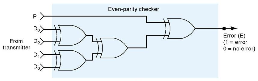
147 Parity Generation and Checking
148 Summary Follow rules to convert representation and symbols between AND/OR Conversions are based on DeMorgan s Law NOR gate implementations are also possible XORs provide straightforward implementation for some functions Used for parity generation and checking XOR circuits AND/ORs can also be implemented using
149 The Problem How can we convert from a circuit drawing to an equation or truth table? Two approaches Create intermediate equations Create intermediate truth tables A B C Out A B C
150 Label Gate Outputs. Label all gate outputs that are functions of input variables 2. Label gates that are functions of input variables and previously labeled gates 3. Repeat process until all outputs are labeled A B C A B C R S T Out
151 Approach : Create Intermediate Equations Step : Create an equation for each gate output based on its inputs R = ABC S=A+B T = C S Out = R + T A B C A B C R S T Out
152 Approach : Substitute in subexpressions Step 2: Form a relationship based on input variables R = ABC S=A+B T = C S = C (A + B) Out = R+T = ABC + C (A+B) A B C A B C R S T Out
153 Approach : Substitute in subexpressions Step 3: Expand equation to SOP Out = ABC + C (A+B) = ABC + AC + BC A B C Out A C B C
154 Approach 2: Truth Table Step : Determine outputs for functions of input variables A B C A B C R S T A B C Out R S
155 Approach 2: Truth Table Step 2: Determine outputs for A B functions of intermediate variables. T = S C A R C C R B C A B C S T Out S T
156 Approach 2: Truth Table Step 3: Determine outputs for function. A Out = R + T A B C A B C R S T B C R S Out T Out
157 More Difficult Example Note labels on interior nodes
158 More Difficult Example: Truth Table Remember to determine intermediate variables starting from the inputs When all inputs are determined for a gate, determine its output The truth table can be reduced using K-maps A B C F2 F 2 T T2 T3 F
159 Summary Important to be able to convert circuits into truth table and equation form WHY? Leads to minimized sum of products representation Two approaches illustrated Approach : Create an equation with circuit outputs dependent on circuit inputs Approach 2: Create a truth table which shows relationship between circuit inputs and circuit outputs Both results can then be minimized using K-maps
ENGIN 112 Intro to Electrical and Computer Engineering
 ENGIN 2 Intro to Electrical and Computer Engineering Lecture 5 Boolean Algebra Overview Logic functions with s and s Building digital circuitry Truth tables Logic symbols and waveforms Boolean algebra
 Get Free notes at Module-I One s Complement: Complement all the bits.i.e. makes all 1s as 0s and all 0s as 1s Two s Complement: One s complement+1 SIGNED BINARY NUMBERS Positive integers (including zero)
IT 201 Digital System Design Module II Notes
 IT 201 Digital System Design Module II Notes BOOLEAN OPERATIONS AND EXPRESSIONS Variable, complement, and literal are terms used in Boolean algebra. A variable is a symbol used to represent a logical quantity.
DIGITAL SYSTEM DESIGN
 DIGITAL SYSTEM DESIGN UNIT I: Introduction to Number Systems and Boolean Algebra Digital and Analog Basic Concepts, Some history of Digital Systems-Introduction to number systems, Binary numbers, Number
Gate Level Minimization Map Method
 Gate Level Minimization Map Method Complexity of hardware implementation is directly related to the complexity of the algebraic expression Truth table representation of a function is unique Algebraically
Lecture 2: Number Systems
 Lecture 2: Number Systems Syed M. Mahmud, Ph.D ECE Department Wayne State University Original Source: Prof. Russell Tessier of University of Massachusetts Aby George of Wayne State University Contents
Combinational Logic & Circuits
 Week-I Combinational Logic & Circuits Spring' 232 - Logic Design Page Overview Binary logic operations and gates Switching algebra Algebraic Minimization Standard forms Karnaugh Map Minimization Other
Chapter 2 Boolean algebra and Logic Gates
 Chapter 2 Boolean algebra and Logic Gates 2. Introduction In working with logic relations in digital form, we need a set of rules for symbolic manipulation which will enable us to simplify complex expressions
Specifying logic functions
 CSE4: Components and Design Techniques for Digital Systems Specifying logic functions Instructor: Mohsen Imani Slides from: Prof.Tajana Simunic and Dr.Pietro Mercati We have seen various concepts: Last
Chapter 3. Gate-Level Minimization. Outlines
 Chapter 3 Gate-Level Minimization Introduction The Map Method Four-Variable Map Five-Variable Map Outlines Product of Sums Simplification Don t-care Conditions NAND and NOR Implementation Other Two-Level
Chapter 2. Boolean Expressions:
 Chapter 2 Boolean Expressions: A Boolean expression or a function is an expression which consists of binary variables joined by the Boolean connectives AND and OR along with NOT operation. Any Boolean
Combinational Logic Circuits
 Chapter 2 Combinational Logic Circuits J.J. Shann (Slightly trimmed by C.P. Chung) Chapter Overview 2-1 Binary Logic and Gates 2-2 Boolean Algebra 2-3 Standard Forms 2-4 Two-Level Circuit Optimization
Gate Level Minimization
 Gate Level Minimization By Dr. M. Hebaishy Digital Logic Design Ch- Simplifying Boolean Equations Example : Y = AB + AB Example 2: = B (A + A) T8 = B () T5 = B T Y = A(AB + ABC) = A (AB ( + C ) ) T8 =
Code No: R Set No. 1
 Code No: R059210504 Set No. 1 II B.Tech I Semester Supplementary Examinations, February 2007 DIGITAL LOGIC DESIGN ( Common to Computer Science & Engineering, Information Technology and Computer Science
UNIT-4 BOOLEAN LOGIC. NOT Operator Operates on single variable. It gives the complement value of variable.
 UNIT-4 BOOLEAN LOGIC Boolean algebra is an algebra that deals with Boolean values((true and FALSE). Everyday we have to make logic decisions: Should I carry the book or not?, Should I watch TV or not?
CS8803: Advanced Digital Design for Embedded Hardware
 CS883: Advanced Digital Design for Embedded Hardware Lecture 2: Boolean Algebra, Gate Network, and Combinational Blocks Instructor: Sung Kyu Lim (limsk@ece.gatech.edu) Website: http://users.ece.gatech.edu/limsk/course/cs883
ELCT201: DIGITAL LOGIC DESIGN
 ELCT201: DIGITAL LOGIC DESIGN Dr. Eng. Haitham Omran, haitham.omran@guc.edu.eg Dr. Eng. Wassim Alexan, wassim.joseph@guc.edu.eg Lecture 3 Following the slides of Dr. Ahmed H. Madian محرم 1439 ه Winter
Experiment 3: Logic Simplification
 Module: Logic Design Name:... University no:.. Group no:. Lab Partner Name: Mr. Mohamed El-Saied Experiment : Logic Simplification Objective: How to implement and verify the operation of the logical functions
X Y Z F=X+Y+Z
 This circuit is used to obtain the compliment of a value. If X = 0, then X = 1. The truth table for NOT gate is : X X 0 1 1 0 2. OR gate : The OR gate has two or more input signals but only one output
ELCT201: DIGITAL LOGIC DESIGN
 ELCT201: DIGITAL LOGIC DESIGN Dr. Eng. Haitham Omran, haitham.omran@guc.edu.eg Dr. Eng. Wassim Alexan, wassim.joseph@guc.edu.eg Lecture 3 Following the slides of Dr. Ahmed H. Madian ذو الحجة 1438 ه Winter
Gate-Level Minimization
 Gate-Level Minimization ( 范倫達 ), Ph. D. Department of Computer Science National Chiao Tung University Taiwan, R.O.C. Fall, 2011 ldvan@cs.nctu.edu.tw http://www.cs.nctu.edu.tw/~ldvan/ Outlines The Map Method
Code No: 07A3EC03 Set No. 1
 Code No: 07A3EC03 Set No. 1 II B.Tech I Semester Regular Examinations, November 2008 SWITCHING THEORY AND LOGIC DESIGN ( Common to Electrical & Electronic Engineering, Electronics & Instrumentation Engineering,
Code No: R Set No. 1
 Code No: R059210504 Set No. 1 II B.Tech I Semester Regular Examinations, November 2006 DIGITAL LOGIC DESIGN ( Common to Computer Science & Engineering, Information Technology and Computer Science & Systems
B.Tech II Year I Semester (R13) Regular Examinations December 2014 DIGITAL LOGIC DESIGN
 Regular Examinations December 2014 DIGITAL LOGIC DESIGN") B.Tech II Year I Semester () Regular Examinations December 2014 (Common to IT and CSE) (a) If 1010 2 + 10 2 = X 10, then X is ----- Write the first 9 decimal digits in base 3. (c) What is meant by don
B.Tech II Year I Semester () Regular Examinations December 2014 (Common to IT and CSE) (a) If 1010 2 + 10 2 = X 10, then X is ----- Write the first 9 decimal digits in base 3. (c) What is meant by don
Gate-Level Minimization
 MEC520 디지털공학 Gate-Level Minimization Jee-Hwan Ryu School of Mechanical Engineering Gate-Level Minimization-The Map Method Truth table is unique Many different algebraic expression Boolean expressions may
Unit-IV Boolean Algebra
 Unit-IV Boolean Algebra Boolean Algebra Chapter: 08 Truth table: Truth table is a table, which represents all the possible values of logical variables/statements along with all the possible results of
2.6 BOOLEAN FUNCTIONS
 2.6 BOOLEAN FUNCTIONS Binary variables have two values, either 0 or 1. A Boolean function is an expression formed with binary variables, the two binary operators AND and OR, one unary operator NOT, parentheses
DKT 122/3 DIGITAL SYSTEM 1
 Company LOGO DKT 122/3 DIGITAL SYSTEM 1 BOOLEAN ALGEBRA (PART 2) Boolean Algebra Contents Boolean Operations & Expression Laws & Rules of Boolean algebra DeMorgan s Theorems Boolean analysis of logic circuits
R.M.D. ENGINEERING COLLEGE R.S.M. Nagar, Kavaraipettai
 L T P C R.M.D. ENGINEERING COLLEGE R.S.M. Nagar, Kavaraipettai- 601206 DEPARTMENT OF ELECTRONICS AND COMMUNICATION ENGINEERING EC8392 UNIT - I 3 0 0 3 OBJECTIVES: To present the Digital fundamentals, Boolean
Gate-Level Minimization. BME208 Logic Circuits Yalçın İŞLER
 Gate-Level Minimization BME28 Logic Circuits Yalçın İŞLER islerya@yahoo.com http://me.islerya.com Complexity of Digital Circuits Directly related to the complexity of the algebraic expression we use to
Boolean Algebra and Logic Gates
 Boolean Algebra and Logic Gates Binary logic is used in all of today's digital computers and devices Cost of the circuits is an important factor Finding simpler and cheaper but equivalent circuits can
Assignment (3-6) Boolean Algebra and Logic Simplification - General Questions
 Boolean Algebra and Logic Simplification - General Questions") Assignment (3-6) Boolean Algebra and Logic Simplification - General Questions 1. Convert the following SOP expression to an equivalent POS expression. 2. Determine the values of A, B, C, and D that make
Assignment (3-6) Boolean Algebra and Logic Simplification - General Questions 1. Convert the following SOP expression to an equivalent POS expression. 2. Determine the values of A, B, C, and D that make
Code No: R Set No. 1
 Code No: R059210504 Set No. 1 II B.Tech I Semester Regular Examinations, November 2007 DIGITAL LOGIC DESIGN ( Common to Computer Science & Engineering, Information Technology and Computer Science & Systems
1. Mark the correct statement(s)
") 1. Mark the correct statement(s) 1.1 A theorem in Boolean algebra: a) Can easily be proved by e.g. logic induction b) Is a logical statement that is assumed to be true, c) Can be contradicted by another
1. Mark the correct statement(s) 1.1 A theorem in Boolean algebra: a) Can easily be proved by e.g. logic induction b) Is a logical statement that is assumed to be true, c) Can be contradicted by another
Combinational Circuits
 Combinational Circuits Combinational circuit consists of an interconnection of logic gates They react to their inputs and produce their outputs by transforming binary information n input binary variables
Injntu.com Injntu.com Injntu.com R16
 1. a) What are the three methods of obtaining the 2 s complement of a given binary (3M) number? b) What do you mean by K-map? Name it advantages and disadvantages. (3M) c) Distinguish between a half-adder
Combinational Logic Circuits
 Chapter 3 Combinational Logic Circuits 12 Hours 24 Marks 3.1 Standard representation for logical functions Boolean expressions / logic expressions / logical functions are expressed in terms of logical
Gate-Level Minimization
 Gate-Level Minimization ( 范倫達 ), Ph. D. Department of Computer Science National Chiao Tung University Taiwan, R.O.C. Fall, 2017 ldvan@cs.nctu.edu.tw http://www.cs.nctu.edu.tw/~ldvan/ Outlines The Map Method
CHAPTER-2 STRUCTURE OF BOOLEAN FUNCTION USING GATES, K-Map and Quine-McCluskey
 CHAPTER-2 STRUCTURE OF BOOLEAN FUNCTION USING GATES, K-Map and Quine-McCluskey 2. Introduction Logic gates are connected together to produce a specified output for certain specified combinations of input
University of Technology
 University of Technology Lecturer: Dr. Sinan Majid Course Title: microprocessors 4 th year Lecture 5 & 6 Minimization with Karnaugh Maps Karnaugh maps lternate way of representing oolean function ll rows
NH 67, Karur Trichy Highways, Puliyur C.F, Karur District DEPARTMENT OF INFORMATION TECHNOLOGY CS 2202 DIGITAL PRINCIPLES AND SYSTEM DESIGN
 NH 67, Karur Trichy Highways, Puliyur C.F, 639 114 Karur District DEPARTMENT OF INFORMATION TECHNOLOGY CS 2202 DIGITAL PRINCIPLES AND SYSTEM DESIGN UNIT 1 BOOLEAN ALGEBRA AND LOGIC GATES Review of binary
Computer Science. Unit-4: Introduction to Boolean Algebra
 Unit-4: Introduction to Boolean Algebra Learning Objective At the end of the chapter students will: Learn Fundamental concepts and basic laws of Boolean algebra. Learn about Boolean expression and will
 www.vidyarthiplus.com Question Paper Code : 31298 B.E./B.Tech. DEGREE EXAMINATION, NOVEMBER/DECEMBER 2013. Third Semester Computer Science and Engineering CS 2202/CS 34/EC 1206 A/10144 CS 303/080230012--DIGITAL
SIDDHARTH GROUP OF INSTITUTIONS :: PUTTUR Siddharth Nagar, Narayanavanam Road QUESTION BANK (DESCRIPTIVE)
") SIDDHARTH GROUP OF INSTITUTIONS :: PUTTUR Siddharth Nagar, Narayanavanam Road 517583 QUESTION BANK (DESCRIPTIVE) Subject with Code : STLD(16EC402) Year & Sem: II-B.Tech & I-Sem Course & Branch: B.Tech
SIDDHARTH GROUP OF INSTITUTIONS :: PUTTUR Siddharth Nagar, Narayanavanam Road 517583 QUESTION BANK (DESCRIPTIVE) Subject with Code : STLD(16EC402) Year & Sem: II-B.Tech & I-Sem Course & Branch: B.Tech
Incompletely Specified Functions with Don t Cares 2-Level Transformation Review Boolean Cube Karnaugh-Map Representation and Methods Examples
 Lecture B: Logic Minimization Incompletely Specified Functions with Don t Cares 2-Level Transformation Review Boolean Cube Karnaugh-Map Representation and Methods Examples Incompletely specified functions
2.1 Binary Logic and Gates
 1 EED2003 Digital Design Presentation 2: Boolean Algebra Asst. Prof.Dr. Ahmet ÖZKURT Asst. Prof.Dr Hakkı T. YALAZAN Based on the Lecture Notes by Jaeyoung Choi choi@comp.ssu.ac.kr Fall 2000 2.1 Binary
EE292: Fundamentals of ECE
 EE292: Fundamentals of ECE Fall 2012 TTh 10:00-11:15 SEB 1242 Lecture 22 121115 http://www.ee.unlv.edu/~b1morris/ee292/ 2 Outline Review Binary Number Representation Binary Arithmetic Combinatorial Logic
SIR C.R.REDDY COLLEGE OF ENGINEERING, ELURU DEPARTMENT OF INFORMATION TECHNOLOGY LESSON PLAN
 SIR C.R.REDDY COLLEGE OF ENGINEERING, ELURU DEPARTMENT OF INFORMATION TECHNOLOGY LESSON PLAN SUBJECT: CSE 2.1.6 DIGITAL LOGIC DESIGN CLASS: 2/4 B.Tech., I SEMESTER, A.Y.2017-18 INSTRUCTOR: Sri A.M.K.KANNA
VALLIAMMAI ENGINEERING COLLEGE. SRM Nagar, Kattankulathur DEPARTMENT OF ELECTRONICS AND COMMUNICATION ENGINEERING EC6302 DIGITAL ELECTRONICS
 VALLIAMMAI ENGINEERING COLLEGE SRM Nagar, Kattankulathur-603 203 DEPARTMENT OF ELECTRONICS AND COMMUNICATION ENGINEERING EC6302 DIGITAL ELECTRONICS YEAR / SEMESTER: II / III ACADEMIC YEAR: 2015-2016 (ODD
D I G I T A L C I R C U I T S E E
 D I G I T A L C I R C U I T S E E Digital Circuits Basic Scope and Introduction This book covers theory solved examples and previous year gate question for following topics: Number system, Boolean algebra,
 Class Subject Code Subject Prepared By Lesson Plan for Time: Lesson. No 1.CONTENT LIST: Introduction to UnitI 2. SKILLS ADDRESSED: Listening I year, 02 sem CS6201 Digital Principles & System Design S.Seedhanadevi
END-TERM EXAMINATION
 (Please Write your Exam Roll No. immediately) END-TERM EXAMINATION DECEMBER 2006 Exam. Roll No... Exam Series code: 100919DEC06200963 Paper Code: MCA-103 Subject: Digital Electronics Time: 3 Hours Maximum
2008 The McGraw-Hill Companies, Inc. All rights reserved.
 28 The McGraw-Hill Companies, Inc. All rights reserved. 28 The McGraw-Hill Companies, Inc. All rights reserved. All or Nothing Gate Boolean Expression: A B = Y Truth Table (ee next slide) or AB = Y 28
LOGIC DESIGN. Dr. Mahmoud Abo_elfetouh
 LOGIC DESIGN Dr. Mahmoud Abo_elfetouh Course objectives This course provides you with a basic understanding of what digital devices are, how they operate, and how they can be designed to perform useful
Digital Techniques. Lecture 1. 1 st Class
 Digital Techniques Lecture 1 1 st Class Digital Techniques Digital Computer and Digital System: Digital computer is a part of digital system, it based on binary system. A block diagram of digital computer
Digital logic fundamentals. Question Bank. Unit I
 Digital logic fundamentals Question Bank Subject Name : Digital Logic Fundamentals Subject code: CA102T Staff Name: R.Roseline Unit I 1. What is Number system? 2. Define binary logic. 3. Show how negative
SUBJECT CODE: IT T35 DIGITAL SYSTEM DESIGN YEAR / SEM : 2 / 3
 UNIT - I PART A (2 Marks) 1. Using Demorgan s theorem convert the following Boolean expression to an equivalent expression that has only OR and complement operations. Show the function can be implemented
II/IV B.Tech (Regular/Supplementary) DEGREE EXAMINATION. Answer ONE question from each unit.
 DEGREE EXAMINATION. Answer ONE question from each unit.") Hall Ticket Number: 14CS IT303 November, 2017 Third Semester Time: Three Hours Answer Question No.1 compulsorily. II/IV B.Tech (Regular/Supplementary) DEGREE EXAMINATION Common for CSE & IT Digital Logic
Hall Ticket Number: 14CS IT303 November, 2017 Third Semester Time: Three Hours Answer Question No.1 compulsorily. II/IV B.Tech (Regular/Supplementary) DEGREE EXAMINATION Common for CSE & IT Digital Logic
UNIT II. Circuit minimization
 UNIT II Circuit minimization The complexity of the digital logic gates that implement a Boolean function is directly related to the complexity of the algebraic expression from which the function is implemented.
BINARY SYSTEM. Binary system is used in digital systems because it is:
 CHAPTER 2 CHAPTER CONTENTS 2.1 Binary System 2.2 Binary Arithmetic Operation 2.3 Signed & Unsigned Numbers 2.4 Arithmetic Operations of Signed Numbers 2.5 Hexadecimal Number System 2.6 Octal Number System
Logic Design: Part 2
 Orange Coast College Business Division Computer Science Department CS 6- Computer Architecture Logic Design: Part 2 Where are we? Number systems Decimal Binary (and related Octal and Hexadecimal) Binary
Simplification of Boolean Functions
 Simplification of Boolean Functions Contents: Why simplification? The Map Method Two, Three, Four and Five variable Maps. Simplification of two, three, four and five variable Boolean function by Map method.
DHANALAKSHMI SRINIVASAN COLLEGE OF ENGINEERING AND TECHNOLOGY
 DHANALAKSHMI SRINIVASAN COLLEGE OF ENGINEERING AND TECHNOLOGY Dept/Sem: II CSE/03 DEPARTMENT OF ECE CS8351 DIGITAL PRINCIPLES AND SYSTEM DESIGN UNIT I BOOLEAN ALGEBRA AND LOGIC GATES PART A 1. How many
MGU-BCA-205- Second Sem- Core VI- Fundamentals of Digital Systems- MCQ s. 2. Why the decimal number system is also called as positional number system?
 MGU-BCA-205- Second Sem- Core VI- Fundamentals of Digital Systems- MCQ s Unit-1 Number Systems 1. What does a decimal number represents? A. Quality B. Quantity C. Position D. None of the above 2. Why the
Gate-Level Minimization. section instructor: Ufuk Çelikcan
 Gate-Level Minimization section instructor: Ufuk Çelikcan Compleity of Digital Circuits Directly related to the compleity of the algebraic epression we use to build the circuit. Truth table may lead to
BOOLEAN ALGEBRA. Logic circuit: 1. From logic circuit to Boolean expression. Derive the Boolean expression for the following circuits.
 COURSE / CODE DIGITAL SYSTEMS FUNDAMENTAL (ECE 421) DIGITAL ELECTRONICS FUNDAMENTAL (ECE 422) BOOLEAN ALGEBRA Boolean Logic Boolean logic is a complete system for logical operations. It is used in countless
Question No: 1 ( Marks: 1 ) - Please choose one A SOP expression is equal to 1
 - Please choose one A SOP expression is equal to 1") ASSALAM O ALAIKUM all fellows ALL IN ONE Mega File CS302 Midterm PAPERS, MCQz & subjective Created BY Farhan& Ali BS (cs) 3rd sem Hackers Group Mandi Bahauddin Remember us in your prayers Mindhacker124@gmail.com
ASSALAM O ALAIKUM all fellows ALL IN ONE Mega File CS302 Midterm PAPERS, MCQz & subjective Created BY Farhan& Ali BS (cs) 3rd sem Hackers Group Mandi Bahauddin Remember us in your prayers Mindhacker124@gmail.com
Points Addressed in this Lecture. Standard form of Boolean Expressions. Lecture 4: Logic Simplication & Karnaugh Map
 Points Addressed in this Lecture Lecture 4: Logic Simplication & Karnaugh Map Professor Peter Cheung Department of EEE, Imperial College London Standard form of Boolean Expressions Sum-of-Products (SOP),
COPYRIGHTED MATERIAL INDEX
 INDEX Absorption law, 31, 38 Acyclic graph, 35 tree, 36 Addition operators, in VHDL (VHSIC hardware description language), 192 Algebraic division, 105 AND gate, 48 49 Antisymmetric, 34 Applicable input
Microcomputers. Outline. Number Systems and Digital Logic Review
 Microcomputers Number Systems and Digital Logic Review Lecture 1-1 Outline Number systems and formats Common number systems Base Conversion Integer representation Signed integer representation Binary coded
R10. II B. Tech I Semester, Supplementary Examinations, May
 SET - 1 1. a) Convert the following decimal numbers into an equivalent binary numbers. i) 53.625 ii) 4097.188 iii) 167 iv) 0.4475 b) Add the following numbers using 2 s complement method. i) -48 and +31
COMBINATIONAL LOGIC CIRCUITS
 COMBINATIONAL LOGIC CIRCUITS 4.1 INTRODUCTION The digital system consists of two types of circuits, namely: (i) Combinational circuits and (ii) Sequential circuits A combinational circuit consists of logic
QUESTION BANK FOR TEST
 CSCI 2121 Computer Organization and Assembly Language PRACTICE QUESTION BANK FOR TEST 1 Note: This represents a sample set. Please study all the topics from the lecture notes. Question 1. Multiple Choice
INSTITUTE OF AERONAUTICAL ENGINEERING (Autonomous) Dundigal, Hyderabad
 Dundigal, Hyderabad") INSTITUTE OF AERONAUTICAL ENGINEERING (Autonomous) Dundigal, Hyderabad - 500043 Course Name : DIGITAL LOGIC DESISN Course Code : AEC020 Class : B Tech III Semester Branch : CSE Academic Year : 2018 2019
INSTITUTE OF AERONAUTICAL ENGINEERING (Autonomous) Dundigal, Hyderabad - 500043 Course Name : DIGITAL LOGIC DESISN Course Code : AEC020 Class : B Tech III Semester Branch : CSE Academic Year : 2018 2019
Computer Logical Organization Tutorial
 Computer Logical Organization Tutorial COMPUTER LOGICAL ORGANIZATION TUTORIAL Simply Easy Learning by tutorialspoint.com tutorialspoint.com i ABOUT THE TUTORIAL Computer Logical Organization Tutorial Computer
Module -7. Karnaugh Maps
 1 Module -7 Karnaugh Maps 1. Introduction 2. Canonical and Standard forms 2.1 Minterms 2.2 Maxterms 2.3 Canonical Sum of Product or Sum-of-Minterms (SOM) 2.4 Canonical product of sum or Product-of-Maxterms(POM)
UNIT- V COMBINATIONAL LOGIC DESIGN
 UNIT- V COMBINATIONAL LOGIC DESIGN NOTE: This is UNIT-V in JNTUK and UNIT-III and HALF PART OF UNIT-IV in JNTUA SYLLABUS (JNTUK)UNIT-V: Combinational Logic Design: Adders & Subtractors, Ripple Adder, Look
Experiment 4 Boolean Functions Implementation
 Experiment 4 Boolean Functions Implementation Introduction: Generally you will find that the basic logic functions AND, OR, NAND, NOR, and NOT are not sufficient to implement complex digital logic functions.
Digital Systems and Binary Numbers
 Digital Systems and Binary Numbers Prof. Wangrok Oh Dept. of Information Communications Eng. Chungnam National University Prof. Wangrok Oh(CNU) 1 / 51 Overview 1 Course Summary 2 Binary Numbers 3 Number-Base
Ch. 5 : Boolean Algebra &
 Ch. 5 : Boolean Algebra & Reduction elektronik@fisika.ui.ac.id Objectives Should able to: Write Boolean equations for combinational logic applications. Utilize Boolean algebra laws and rules for simplifying
VALLIAMMAI ENGINEERING COLLEGE
 VALLIAMMAI ENGINEERING COLLEGE SRM Nagar, Kattankulathur 603 203 DEPARTMENT OF INFORMATION TECHNOLOGY & COMPUTER SCIENCE AND ENGINEERING QUESTION BANK II SEMESTER CS6201- DIGITAL PRINCIPLE AND SYSTEM DESIGN
INSTITUTE OF AERONAUTICAL ENGINEERING (Autonomous) Dundigal, Hyderabad
 Dundigal, Hyderabad") INSTITUTE OF AERONAUTICAL ENGINEERING (Autonomous) Dundigal, Hyderabad - 500 043 COMPUTER SCIENCE AND ENGINEERING TUTORIAL QUESTION BANK Name : DIGITAL LOGIC DESISN Code : AEC020 Class : B Tech III Semester
INSTITUTE OF AERONAUTICAL ENGINEERING (Autonomous) Dundigal, Hyderabad - 500 043 COMPUTER SCIENCE AND ENGINEERING TUTORIAL QUESTION BANK Name : DIGITAL LOGIC DESISN Code : AEC020 Class : B Tech III Semester
Chapter 2 Combinational Logic Circuits
 Logic and Computer Design Fundamentals Chapter 2 Combinational Logic Circuits Part 2 Circuit Optimization Overview Part Gate Circuits and Boolean Equations Binary Logic and Gates Boolean Algebra Standard
ENGINEERS ACADEMY. 7. Given Boolean theorem. (a) A B A C B C A B A C. (b) AB AC BC AB BC. (c) AB AC BC A B A C B C.
 A B A C B C A B A C. (b) AB AC BC AB BC. (c) AB AC BC A B A C B C.") Digital Electronics Boolean Function QUESTION BANK. The Boolean equation Y = C + C + C can be simplified to (a) (c) A (B + C) (b) AC (d) C. The Boolean equation Y = (A + B) (A + B) can be simplified to
Digital Electronics Boolean Function QUESTION BANK. The Boolean equation Y = C + C + C can be simplified to (a) (c) A (B + C) (b) AC (d) C. The Boolean equation Y = (A + B) (A + B) can be simplified to
Introduction to Computer Architecture
 Boolean Operators The Boolean operators AND and OR are binary infix operators (that is, they take two arguments, and the operator appears between them.) A AND B D OR E We will form Boolean Functions of
數位系統 Digital Systems 朝陽科技大學資工系. Speaker: Fuw-Yi Yang 楊伏夷. 伏夷非征番, 道德經察政章 (Chapter 58) 伏者潛藏也道紀章 (Chapter 14) 道無形象, 視之不可見者曰夷
 伏者潛藏也道紀章 (Chapter 14) 道無形象, 視之不可見者曰夷") 數位系統 Digital Systems Department of Computer Science and Information Engineering, Chaoyang University of Technology 朝陽科技大學資工系 Speaker: Fuw-Yi Yang 楊伏夷 伏夷非征番, 道德經察政章 (Chapter 58) 伏者潛藏也道紀章 (Chapter 14) 道無形象,
數位系統 Digital Systems Department of Computer Science and Information Engineering, Chaoyang University of Technology 朝陽科技大學資工系 Speaker: Fuw-Yi Yang 楊伏夷 伏夷非征番, 道德經察政章 (Chapter 58) 伏者潛藏也道紀章 (Chapter 14) 道無形象,
CDA 3200 Digital Systems. Instructor: Dr. Janusz Zalewski Developed by: Dr. Dahai Guo Spring 2012
 CDA 3200 Digital Systems Instructor: Dr. Janusz Zalewski Developed by: Dr. Dahai Guo Spring 2012 Outline Data Representation Binary Codes Why 6-3-1-1 and Excess-3? Basic Operations of Boolean Algebra Examples
R07
 www..com www..com SET - 1 II B. Tech I Semester Supplementary Examinations May 2013 SWITCHING THEORY AND LOGIC DESIGN (Com. to EEE, EIE, BME, ECC) Time: 3 hours Max. Marks: 80 Answer any FIVE Questions
Binary. Hexadecimal BINARY CODED DECIMAL
 Logical operators Common arithmetic operators, like plus, minus, multiply and divide, works in any number base but the binary number system provides some further operators, called logical operators. Meaning
CMPE223/CMSE222 Digital Logic
 CMPE223/CMSE222 Digital Logic Optimized Implementation of Logic Functions: Strategy for Minimization, Minimum Product-of-Sums Forms, Incompletely Specified Functions Terminology For a given term, each
Simplification of Boolean Functions
 COM111 Introduction to Computer Engineering (Fall 2006-2007) NOTES 5 -- page 1 of 5 Introduction Simplification of Boolean Functions You already know one method for simplifying Boolean expressions: Boolean
DIGITAL ARITHMETIC: OPERATIONS AND CIRCUITS
 C H A P T E R 6 DIGITAL ARITHMETIC: OPERATIONS AND CIRCUITS OUTLINE 6- Binary Addition 6-2 Representing Signed Numbers 6-3 Addition in the 2 s- Complement System 6-4 Subtraction in the 2 s- Complement
Digital Logic Design (CEN-120) (3+1)
 (3+1)") Digital Logic Design (CEN-120) (3+1) ASSISTANT PROFESSOR Engr. Syed Rizwan Ali, MS(CAAD)UK, PDG(CS)UK, PGD(PM)IR, BS(CE)PK HEC Certified Master Trainer (MT-FPDP) PEC Certified Professional Engineer (COM/2531)
Digital Logic Design (CEN-120) (3+1) ASSISTANT PROFESSOR Engr. Syed Rizwan Ali, MS(CAAD)UK, PDG(CS)UK, PGD(PM)IR, BS(CE)PK HEC Certified Master Trainer (MT-FPDP) PEC Certified Professional Engineer (COM/2531)
NODIA AND COMPANY. GATE SOLVED PAPER Computer Science Engineering Digital Logic. Copyright By NODIA & COMPANY
 No part of this publication may be reproduced or distributed in any form or any means, electronic, mechanical, photocopying, or otherwise without the prior permission of the author. GATE SOLVED PAPER Computer
Summary. Boolean Addition
 Summary Boolean Addition In Boolean algebra, a variable is a symbol used to represent an action, a condition, or data. A single variable can only have a value of or 0. The complement represents the inverse
DIGITAL ELECTRONICS. Vayu Education of India
 DIGITAL ELECTRONICS ARUN RANA Assistant Professor Department of Electronics & Communication Engineering Doon Valley Institute of Engineering & Technology Karnal, Haryana (An ISO 9001:2008 ) Vayu Education
Chap.3 3. Chap reduces the complexity required to represent the schematic diagram of a circuit Library
 3.1 Combinational Circuits 2 Chap 3. logic circuits for digital systems: combinational vs sequential Combinational Logic Design Combinational Circuit (Chap 3) outputs are determined by the present applied
VALLIAMMAI ENGINEERING COLLEGE
 VALLIAMMAI ENGINEERING COLLEGE SRM Nagar, Kattankulathur 603 203 DEPARTMENT OF INFORMATION TECHNOLOGY QUESTION BANK Academic Year 2018 19 III SEMESTER CS8351-DIGITAL PRINCIPLES AND SYSTEM DESIGN Regulation
1. Draw general diagram of computer showing different logical components (3)
") Tutorial 1 1. Draw general diagram of computer showing different logical components (3) 2. List at least three input devices (1.5) 3. List any three output devices (1.5) 4. Fill the blank cells of the
Tutorial 1 1. Draw general diagram of computer showing different logical components (3) 2. List at least three input devices (1.5) 3. List any three output devices (1.5) 4. Fill the blank cells of the
DIGITAL ELECTRONIC CIRCUITS
 DIGITAL ELECTRONIC CIRCUITS SUBJECT CODE: PEI4I103 B.Tech, Fourth Semester Prepared By Dr. Kanhu Charan Bhuyan Asst. Professor Instrumentation and Electronics Engineering COLLEGE OF ENGINEERING AND TECHNOLOGY