*Instruction Matters: Purdue Academic Course Transformation. Introduction to Digital System Design. Module 4 Arithmetic and Computer Logic Circuits
|
|
|
- Annabelle Lewis
- 5 years ago
- Views:
Transcription

1 Purdue IM:PACT* Fall 2018 Edition *Instruction Matters: Purdue Academic Course Transformation Introduction to Digital System Design Module 4 Arithmetic and Computer Logic Circuits
2 Glossary of Common Terms RADIX a commonly-used signed number notation (also called 2 s complement) OPERAND a binary number involved in an arithmetic or logical operation HALF ADDER logic circuit that adds two binary bits to produce carry and sum outputs FULL ADDER logic circuit that adds three binary bits to produce carry and sum outputs ADDER/SUBTRACTOR logic circuit that adds and subtracts pairs of binary operands MAGNITUDE COMPARATOR logic circuit that determines which binary operand is greater/less than a second binary operand 2
3 Glossary of Common Terms CARRY LOOK-AHEAD a means of generating the carry functions needed for addition in parallel MULTIPLIER logic circuit that multiplies pairs of binary operands COMPUTER device that sequentially executes a stored program PROGRAM a series of instructions that direct the processing activity of a computer INSTRUCTION a unit of processing activity ( line of code ) executed by a computer OPCODE the operation code field of an instruction 3
4 Glossary of Common Terms MEMORY array of D latches used to store instructions, operands, and results PROGRAM COUNTER register that points to the next instruction to execute INSTRUCTION REGISTER register used to stage the instruction fetched from memory ALU arithmetic logic unit, performs arithmetic and logic operations on binary operands INSTRUCTION DECODER & MICROSEQUENCER state machine that orchestrates the activities of a computer s functional blocks 4
5 Glossary of Common Terms MICROSEQUENCE the minute phases of instruction processing by a computer TRANSFER OF CONTROL continue execution of program at a location different than the next consecutive instruction I/O data input and output operations performed by a computer STACK last in, first out data structure used to support expression evaluation and subroutine linkage STACK POINTER register used to point to the top stack item (or next available location) 5
6 Purdue IM:PACT* Fall 2018 Edition *Instruction Matters: Purdue Academic Course Transformation Introduction to Digital System Design Module 4-A Signed Number Notation
7 Reading Assignment: DDPP 4 th Ed., pp Learning Objectives: Compare and contrast three different signed number notations: sign and magnitude, diminished radix, and radix Convert a number from one signed notation to another Describe how to perform sign extension of a number represented using any of the three notation schemes 7
8 Outline Overview Signed number notation Sign and magnitude Diminished radix Radix Comparison chart Simplifications for binary numbers Sign extension 8
9 Overview In order to represent positive and negative numbers as a series of digits without + and signs, various signed number notations have been devised We will discuss the three most commonly used signed number notations: sign and magnitude (SM) diminished radix (DR) radix (R) 9
10 Sign and Magnitude The original signed number convention employed by vacuum tube vintage digijocks was sign and magnitude notation Here the left-most digit (or sign bit ) indicates whether the number is positive or negative: 0 positive R 1 negative (where R is the radix or base of the number) 10
 5 SM(0123) 10 and SM(9123) 10 are referred to as the sign and magnitude complements of one another")
11 Sign and Magnitude Examples: (+123) 10 = SM(0123) 10 ( 123) 10 = SM(9123) 10 (+144) 5 = SM(0144) 5 ( 144) 5 = SM(4144) 5 SM(0123) 10 and SM(9123) 10 are referred to as the sign and magnitude complements of one another 11
12 Sign and Magnitude Negation Method: If N is a number in base R with sign digit n S, such that (N) R = n S n 3 n 2 n 1 n 0 then (N) R = (R 1 n S )n 3 n 2 n 1 n 0 Examples: (+1101) 2 = SM(01101) 2 ( 1101) 2 = SM(11101) 2 12
13 Diminished Radix The negation (or complement) of a number represented in diminished radix (DR) notation can be found by subtracting each digit (including the sign digit) from (R 1), i.e., the radix minus one or the radix diminished by one Examples: (+123) 10 = DR(0123) 10 ( 123) 10 = ( ) 10 = DR(9876) 10 DR(0123) 10 and DR(9876) 10 are referred to as the diminished radix complements of one another. 13
14 Diminished Radix Negation Method: If N is a number in base R, (N) R = (R n 1) R (N) R Examples: (+1101) 2 = DR(01101) 2 ( 1101) 2 = DR(10010) 2 Note that positive DR numbers have the same representation as positive SM numbers; negative DR and SM numbers, however, have different representations 14
15 Radix The negation (or complement) of a number represented in radix (R) notation can be found by adding one to the least significant position of the diminished radix negation of that number Examples: (+123) 10 = R(0123) 10 ( 123) 10 = ( ) 10 = R(9877) 10 R(0123) 10 and R(9877) 10 are referred to as the radix complements of one another 15
16 Radix Negation Method: If N is a number in base R, (N) R = (R n ) R (N) R Examples: (+1101) 2 = R(01101) 2 ( 1101) 2 = R(10011) 2 Note that positive R, DR, and SM numbers all have the same representation; negative R, DR, and SM numbers, however, all have different representations 16
17 Comparison of Signed Number Notations N 10 SM DR R
18 Comparison of Signed Number Notations N 10 SM DR R Radix has no negative zero 4 18
19 Comparison of Signed Number Notations N 10 SM DR R All positive number representations are identical Radix has no negative zero 19
20 Comparison of Signed Number Notations N 10 SM DR R All positive number representations are identical Radix has no negative zero All negative number representations are different 20
21 Comparison of Signed Number Notations N 10 SM DR R All positive number representations are identical Radix has no negative zero All negative number representations are different Radix has an extra negative number 21
22 Simplifications for Binary When finding the negations (complements) of binary (base 2) numbers, the methods simplify as follows: SM: complement the sign position DR (also called 1 s complement ): complement each position R (also called 2 s complement ): add 1 to the DR complement -or- scan number from right to left; complement each position to the left of the first 1 encountered 22
23 Practice If (N) 2 = SM(01100) 2, find (N) 2 SM(11100) 2 If (N) 2 = DR(01100) 2, find (N) 2 DR(10011) 2 If (N) 2 = R(01100) 2, find (N) 2 R(10100) 2 23
24 Sign Extension Sometimes signed numbers of different length (number of bits) need to be added together here, the shorter number needs to be padded with leading digits to make it the two numbers the same length The rules for padding signed numbers with leading digits are as follows: SM: insert as many zeroes as needed to the right of the sign position DR & R: replicate the sign digit as many times as needed 24
25 Practice Extend SM(09345) 10 to 8 digits Extend DR(76500) 8 to 8 digits SM( ) 10 DR( ) 8 Extend R(01100) 2 to 8 digits R( ) 2 Extend R(11100) 2 to 8 digits R( ) 2 25
26 Comparison/Observations SM and DR notation have a balanced set of positive and negative numbers, and have two representations for zero R notation has an unbalanced set of positive and negative numbers (there is an extra negative number ), and has a single representation for zero 99% of all computers use radix notation; our discussion on addition and subtraction will therefore focus on radix arithmetic (we will assume a prefix of R on all numbers subsequently used) 26
27 Clicker Quiz 27
28 1. The five-bit radix number, R(10101) 2, converted to sign and magnitude notation, is: A. SM (10101) 2 B. SM (01010) 2 C. SM (11010) 2 D. SM (11011) 2 E. none of the above 28
29 2. The five-bit diminished radix number, DR(10101) 2, converted to sign and magnitude notation, is: A. SM (10101) 2 B. SM (01010) 2 C. SM (11010) 2 D. SM (11011) 2 E. none of the above 29
30 Purdue IM:PACT* Fall 2018 Edition *Instruction Matters: Purdue Academic Course Transformation Introduction to Digital System Design Module 4-B Radix Addition and Subtraction
31 Reading Assignment: DDPP 4 th Ed., pp Learning Objectives: perform radix addition and subtraction describe the various conditions of interest following an arithmetic operation: overflow, carry, negative, zero 31
32 Outline Radix Addition Overflow Detection Radix Subtraction 32
33 Radix Arithmetic Addition Method: Add all digits, including the sign digits; ignore any carry out of the sign position Problem: Since we are working with numbers of fixed length, the result of an addition can yield a number which is too large to represent in the same number of digits this error condition is called overflow Important: When overflow occurs, there is no valid numeric result 33
34 Overflow Detection Summarization: Overflow occurs if two positive numbers are added and a negative result is obtained, or if two negative numbers are added and a positive result is obtained (or, if numbers of like sign are added and a result with the opposite sign is obtained) Overflow cannot occur when adding numbers of the opposite sign Another way to detect overflow: If the carry in to the sign position is different than the carry out of the sign position, then overflow has occurred 34
35 Radix Arithmetic Addition Examples: (all numbers are binary) Here, added two positive numbers, but got a negative result OVERFLOW 35
36 Radix Arithmetic Addition Examples: (all numbers are binary) Here, added two positive numbers, but got a negative result OVERFLOW Here, added two positive numbers, and got a positive result (+12) OK! 36
37 Radix Arithmetic Addition Examples: (all numbers are binary) ignore Here, added two negative numbers, and got a negative result (-14) OK! 37
38 Radix Arithmetic Addition Examples: (all numbers are binary) ignore ignore Here, added two negative numbers, and got a negative result (-14) OK! Here, added two negative numbers, but got a positive result OVERFLOW 38
39 Radix Arithmetic Addition Examples: (all numbers are binary) ignore Here, added numbers of opposite sign overflow cannot occur (result is +2) 39
40 Radix Arithmetic Addition Examples: (all numbers are binary) ignore Here, added numbers of opposite sign overflow cannot occur (result is +2) Again, added numbers of opposite sign overflow cannot occur (result is -1) 40

41 Radix Arithmetic Subtraction Method: Take the radix complement of the subtrahend and ADD; the same rules for overflow apply Examples: Why does this work? Examples: 5 (+3) = 5 + ( 3) = 2 9 ( 13) = 9 + (+13) = 22 41
42 Radix Arithmetic Subtraction Method: Take the radix complement of the subtrahend and ADD; the same rules for overflow apply Examples: Here, added numbers of opposite sign overflow cannot occur (result is -1) minuend Radix complement of subtrahend 42
43 Radix Arithmetic Subtraction Examples: Overflow 43
44 Radix Arithmetic Subtraction Examples: Overflow ignore Overflow 44
45 Radix Arithmetic Subtraction Examples: ignore
46 Radix Arithmetic Subtraction Examples: ignore
47 Clicker Quiz 47
48 1. When adding the five-bit signed numbers (10111) 2 + (11001) 2 using radix arithmetic, the result obtained is: A. (10000) 2 B. (110000) 2 C. (11000) 2 D. overflow (invalid result) E. none of the above 48
49 2. When subtracting the five-bit signed numbers (10111) 2 - (11001) 2 using radix arithmetic, the result obtained is: A. (10000) 2 B. (11000) 2 C. (11110) 2 D. overflow (invalid result) E. none of the above 49
50 Purdue IM:PACT* Fall 2018 Edition *Instruction Matters: Purdue Academic Course Transformation Introduction to Digital System Design Module 4-C Adder, Subtractor, and Comparator Circuits
51 Reading Assignment: DDPP 4 th Ed., pp , Learning Objectives: Describe the operation of a half-adder and write equations for its sum (S) and carry (C) outputs Describe the operation of a full adder and write equations for its sum (S) and carry (C) outputs Design a population counting or vote counting circuit using an array of half-adders and/or full-adders Design an N-digit radix adder/subtractor circuit with condition codes Design a (signed or unsigned) magnitude comparator circuit that determines if A=B, A<B, or A>B 51
52 Outline Overview Half Adders Full Adders Radix Adder/Subtractors Comparators 52
53 Overview Addition is the most commonly performed arithmetic operation in digital systems An adder combines two arithmetic operands using the addition rules described previously The same addition rules (and circuits) are used for both signed (two s complement) and unsigned numbers Subtraction can be performed by taking the complement of the subtrahend and adding it to the minuend 53
54 Half Adders A half adder is used to add two binary digits, X i and Y i, to form a sum digit, S i, and a carry digit, C i X i Y i C i S i S i = X i Y i C i = X i Y i 54
55 Full Adders A full adder is used to add three binary digits, X i, Y i, C i-1 (where C i-1 is usually the carry in from a previous stage), to form a sum digit, S i, and a carry out digit, C i 55
56 Full Adders X i Y i C i-1 C i S i S i = X i Y i C i-1 C i = X i Y i + X i C i-1 + Y i C i-1 56
57 Example Vote Counting Circuit Using only half adders and full adders, design a circuit that finds the (unsigned) sum of five binary digits X i C i HA Y i S i Y Z V W X i C i Y i X i Y i FA C i-1 FA C i-1 S i S 2 S 1 S 0 C i Also called a population counter S i X V W X Y Z S 2 S 1 S 0 57
58 Clicker Quiz 58
59 The Digi-Vota-Matic is a three-judge score tabulation system that allows each judge to enter a score ranging from 0 (00 2 ) to 3 (11 2 ) on a pair of DIP switches, and displays the sum of the three scores (ranging from 0 to 9 ) on a 7-segment LED. 59
60 1. Implemented using a CASE statement in Verilog, a circuit that finds the sum of three 2-bit unsigned numbers would require assignment statements. A. 16 B. 32 C. 64 D. 128 E. none of the above 60
61 2. Implemented using a 22V10 PLD, a circuit that finds the sum of three 2-bit unsigned numbers would require no more than macrocells. A. 2 B. 4 C. 8 D. 16 E. none of the above 61
62 Multi-Digit Adder/Subtractor Circuits Two binary words, each with n bits, can be added using a ripple adder a cascade of n full-adder stages, each of which handles one bit (also called an iterative circuit) The word ripple describes the flow of the carries from one full adder cell to the next Subtraction is performed by taking the diminished radix complement of the subtrahend (using XOR gates) and setting the least significant bit carry-in (LSB C in ) to 1 (effectively forming the radix complement of the subtrahend) 62
63 Review of Radix Addition Method: Add all digits, including the sign digits; ignore any carry out of the sign position Problem: Since we are working with numbers of fixed length, the result of an addition can yield a number which is too large to represent in the same number of digits this error condition is called overflow Important: When overflow occurs, there is no valid numeric result 63
64 Overflow Detection Summarization: Overflow occurs if two positive numbers are added and a negative result is obtained, or if two negative numbers are added and a positive result is obtained (or, if numbers of like sign are added and a result with the opposite sign is obtained) Overflow cannot occur when adding numbers of the opposite sign Another way to detect overflow: If the carry in to the sign position is different than the carry out of the sign position, then overflow has occurred 64
65 Example 4-bit Ripple Adder/Subtractor ± A 3 A 2 A 1 A 0 B 3 B 2 B 1 B 0 S 3 S 2 S 1 S 0 X i X i C i Y i X i Y i X i Y i FA C i-1 FA C i-1 FA C i-1 FA C i-1 C i Y i S i S i C i S i C i S i 65
66 Example 4-bit Ripple Adder/Subtractor ± A 3 A 2 A 1 A 0 B 3 B 2 B 1 B 0 S 3 S 2 S 1 S 0 X i Y i X i C i Y i X i Y i X i Y i FA C i-1 FA C i-1 FA C i-1 FA C i-1 C i S i S i C i S i C i S i LSB Cin 66
67 Example 4-bit Ripple Adder/Subtractor ± A 3 A 2 A 1 A 0 B 3 B 2 B 1 B 0 S 3 S 2 S 1 S 0 A 3 A 2 A 1 A 0 X i Y i X i C i Y i X i Y i X i Y i FA C i-1 FA C i-1 FA C i-1 FA C i-1 C i S i S i C i S i C i S i LSB Cin S 3 S 2 S 1 S 0 67
68 Example 4-bit Ripple Adder/Subtractor A 3 A 2 A 1 A 0 ± B 3 B 2 B 1 B 0 S 3 S 2 S 1 S 0 M = 0 add 1 subtract M B 3 B 2 B 1 B 0 A 3 A 2 A 1 A 0 X i Y i X i C i Y i X i Y i X i Y i FA C i-1 FA C i-1 FA C i-1 FA C i-1 C i S i S i C i S i C i S i LSB Cin S 3 S 2 S 1 S 0 68
69 Example 4-bit Ripple Adder/Subtractor A 3 A 2 A 1 A 0 ± B 3 B 2 B 1 B 0 S 3 S 2 S 1 S 0 M = 0 add 1 subtract M B 3 B 2 B 1 B 0 A 3 A 2 A 1 A 0 X i Y i X i C i Y i X i Y i X i Y i FA C i-1 FA C i-1 FA C i-1 FA C i-1 C i S i S i C i S i C i S i LSB Cin S 3 S 2 S 1 S 0 V (overflow) 69
70 Other Conditions of Interest In addition to overflow, other conditions of interest following an arithmetic operation include the following: ZERO the result of the computation was 00 0 NEGATIVE the result of the computation was a negative number CARRY the computation produced a carry out of the sign position These conditions are sometimes referred to as condition codes or flags 70
71 Example 4-bit Ripple Adder/Subtractor A 3 A 2 A 1 A 0 ± B 3 B 2 B 1 B 0 S 3 S 2 S 1 S 0 M = 0 add 1 subtract M B 3 B 2 B 1 B 0 A 3 A 2 A 1 A 0 X i Y i X i C i Y i X i Y i X i Y i FA C i-1 FA C i-1 FA C i-1 FA C i-1 C i S i S i C i S i C i S i LSB Cin C S 3 N S 2 S 1 S 0 V (overflow) Z 71
72 Looking Ahead The C (carry) flag serves multiple purposes Extended precision add/subtract ( extended integer multiples of 32 bits, if using a 32-bit processor) Add C bit (being set) represents the presence of a carry propagated forward (from least significant word to most significant word of extended number) Subtract C bit (being set) represents the absence of a borrow propagated forward (i.e., the complement of a borrow propagated forward, which means that C=1 indicates that no borrow is propagated forward) So regardless of whether an add or subtract is performed, the C bit is simply set to the carry out of the sign position Conditional execution (change of flow) Flags set based on subtract of operands being compared (e.g. CMP instruction) 72
73 Looking Ahead ARM extended precision 64-bit addition using (iterative) ADCS (R1) (R1)+(R3)+(CF) 73
-(R3)-(CF) which is equivalent to (R1) (R1)-(R3)+(CF) (CF) is the borrow propagated")
74 Looking Ahead ARM extended precision 64-bit subtraction using (iterative) SBCS (R1) (R1)-(R3)-(CF) which is equivalent to (R1) (R1)-(R3)+(CF) (CF) is the borrow propagated forward 74
75 Clicker Quiz 75
76 1. When performing radix addition, the XOR of the carry in to the sign position with the carry out of the sign position provides a means to: A. generate a carry that is propagated forward B. generate a borrow that is propagated forward C. check for a negative result D. check for an invalid result E. none of the above 76
77 2. Following a subtract operation, the carry flag (C) can be used to: A. generate the complement of a borrow that is propagated forward B. generate a borrow that is propagated forward C. check for a negative result D. check for an invalid result E. none of the above 77
78 3. Following an add operation, the negative flag (N) can be used to: A. generate a carry that is propagated forward B. generate a borrow that is propagated forward C. check for a negative result D. check for an invalid result E. none of the above 78
79 Comparators Comparing two binary words for equality is a commonly used operation in computer systems a circuit that does this is called a comparator XOR and XNOR gates may be viewed as one-bit comparators (from which larger comparators can be built) Circuits that determine an arithmetic relationship between two operands (greater or less than) are called magnitude comparators 79
80 Example 4-bit Magnitude Comparator Design a 4-bit (signed) magnitude comparator that determines if A=B, A<B, or A>B Solution: Calculate (A B) and examine the condition codes produced for each case ZERO ( Z for zero flag) NEGATIVE ( N for negative flag) CARRY ( C for carry/borrow flag) OVERFLOW ( V for overflow flag) Need to know how the condition codes are affected for all possible results generated 80

81 Example 4-bit Magnitude Comparator Step 1: Determine condition codes produced for all possible (2-bit) cases of A B A 1 A 0 (A) B 1 B 0 (B)? C Z N V
82 Example 4-bit Magnitude Comparator Step 1: Determine condition codes produced for all possible (2-bit) cases of A B A 1 A 0 (A) B 1 B 0 (B)? C Z N V
83 Example 4-bit Magnitude Comparator Step 1: Determine condition codes produced for all possible (2-bit) cases of A B A 1 A 0 (A) B 1 B 0 (B)? C Z N V (A) = (B) (A) < (B) (A) > (B) (A) > (B) (A) > (B) (A) = (B) (A) > (B) (A) > (B) (A) < (B) (A) < (B) (A) = (B) (A) < (B) (A) < (B) (A) < (B) (A) > (B) (A) = (B)
84 Example 4-bit Magnitude Comparator Step 2: Make note of the condition code combinations corresponding to the functions A=B, A<B, and A>B A 1 A 0 (A) B 1 B 0 (B)? C Z N V (A) = (B) (A) < (B) (A) > (B) (A) > (B) (A) > (B) (A) = (B) (A) > (B) (A) > (B) (A) < (B) (A) < (B) (A) = (B) (A) < (B) (A) < (B) (A) < (B) (A) > (B) (A) = (B)
85 Example 4-bit Magnitude Comparator Step 2: Make note of the condition code combinations corresponding to the functions A=B, A<B, and A>B A 1 A 0 (A) B 1 B 0 (B)? C Z N V (A) = (B) (A) < (B) (A) > (B) (A) > (B) (A) > (B) (A) = (B) (A) > (B) (A) > (B) (A) < (B) (A) < (B) (A) = (B) (A) < (B) (A) < (B) (A) < (B) (A) > (B) (A) = (B)
86 Example 4-bit Magnitude Comparator Step 2: Make note of the condition code combinations corresponding to the functions A=B, A<B, and A>B A 1 A 0 (A) B 1 B 0 (B)? C Z N V (A) = (B) (A) < (B) (A) > (B) (A) > (B) (A) > (B) (A) = (B) (A) > (B) (A) > (B) (A) < (B) (A) < (B) (A) = (B) (A) < (B) (A) < (B) (A) < (B) (A) > (B) (A) = (B)
87 Example 4-bit Magnitude Comparator Step 3: Observe that F A=B = Z A 1 A 0 (A) B 1 B 0 (B)? C Z N V (A) = (B) (A) < (B) (A) > (B) (A) > (B) (A) > (B) (A) = (B) (A) > (B) (A) > (B) (A) < (B) (A) < (B) (A) = (B) (A) < (B) (A) < (B) (A) < (B) (A) > (B) (A) = (B)
88 Example 4-bit Magnitude Comparator Step 4: Map and minimize the function for F A<B A 1 A 0 (A) B 1 B 0 (B)? C Z N V (A) = (B) (A) < (B) (A) > (B) (A) > (B) (A) > (B) (A) = (B) (A) > (B) (A) > (B) (A) < (B) (A) < (B) (A) = (B) (A) < (B) (A) < (B) (A) < (B) (A) > (B) (A) = (B) C C d 0 0 N d d d d d d N d d 1 Z Z Z F A<B = N V V V V 88
89 Example 4-bit Magnitude Comparator Step 5: Map and minimize the function for F A>B A 1 A 0 (A) B 1 B 0 (B)? C Z N V (A) = (B) (A) < (B) (A) > (B) (A) > (B) (A) > (B) (A) = (B) (A) > (B) (A) > (B) (A) < (B) (A) < (B) (A) = (B) (A) < (B) (A) < (B) (A) < (B) (A) > (B) (A) = (B) C C d 0 1 N d d d d d d N d d 0 V V V Z Z Z F A>B = V N + V N Z 89
90 Example 4-bit Ripple Adder/Subtractor A 3 A 2 A 1 A 0 C B 3 B 2 B 1 B N F A<B = N V 0 V S 3 S 2 S 1 S Z F A>B = V N + V N Z 0 B 3 B 2 B 1 B 0 A 3 A 2 A 1 A 0 X i Y i X i C i Y i X i Y i X i Y i FA C i-1 FA C i-1 FA C i-1 FA C i-1 C i S i S i C i S i C i S i 1 C S 3 N S 2 V (overflow) S 1 S 0 F A=B = Z 90
91 Purdue IM:PACT* Fall 2018 Edition *Instruction Matters: Purdue Academic Course Transformation Introduction to Digital System Design Module 4-D Carry Look-Ahead Adder Circuits
92 Reading Assignment: DDPP 4 th Ed., pp , , Instructional Objectives: Describe the operation of a carry look-ahead (CLA) adder circuit, and compare its performance to that of a ripple adder circuit Define the CLA propagate (P) and generate (G) functions, and show how they can be realized using a half-adder Write the equation for the carry out function of an arbitrary CLA bit position Draw a diagram depicting the overall organization of a CLA Determine the worst case propagation delay incurred by a practical (PLD-based) realization of a CLA Describe how a group ripple adder can be constructed using N-bit CLA blocks 92
93 Outline Overview CLA derivation CLA organization Sample CLA realization in Verilog Observations 93
94 Overview Previously we looked at one method of constructing an n-digit binary adder from n full adders: connecting the carry out from one stage to the carry in of the next in a ripple fashion For large values of n, the propagation delay of a ripple adder can be excessive A significant speed-up could be obtained by calculating the carries in parallel, rather than iteratively a design that accomplishes this goal is the carry look-ahead (CLA) adder circuit (look-ahead anticipated) 94
95 CLA Derivation Consider the 4-bit binary adder: Stage: Augend: X3 X2 X1 X0 Addend: Y3 Y2 Y1 Y0 Sum: S3 S2 S1 S0 95
96 CLA Derivation Definition: The generate function G i = 1 if there is a carry out of stage i regardless of whether or not there is a carry in to stage i (i.e., both X i and Y i are 1) G i = X i Y i Definition: The propagate function P i = 1 if a carry in to stage i will cause a carry out of stage i (i.e., either X i = 0 and Y i = 1 or X i = 1 and Y i = 0) P i = X i Y i NOTE: Another valid definition of P i is X i +Y i the XOR definition leads to some CLA circuit simplifications, however 96
97 CLA Derivation Illustration of propagate and generate 1 1 x 1 1 x + x 0 1 x Generate from stage 1 Propagated by stage 2 97
98 CLA Derivation Note that the P i and G i functions can be generated using a half adder X i Y i C i S i P i = S i = X i Y i G i = C i = X i Y i 98
99 CLA Derivation Next we would like to write our basic full adder equations in terms of propagate and generate functions To do this, we will need to reexamine the K-maps for the sum and carry equations of the full adder 99
100 Full Adder Review X i Y i C i-1 C i S i
101 Full Adder Review Map of sum function: C i-1 C i-1 X X Y Y Y S i = X i Y i C i-1 = P i C i-1 101
102 Full Adder Review Map of carry function: C i-1 C i-1 X X Y Y Y C i = X i Y i + C i-1 (X i Y i ) = G i + C i-1 P i 102
103 CLA Derivation Rewriting the equations for our 4-bit binary adder, we obtain the following: C -1 = C in C 0 = G 0 + C in P 0 C 1 = G 1 + C 0 P 1 C 2 = G 2 + C 1 P 2 C 3 = C out = G 3 + C 2 P 3 103
104 CLA Derivation We would like to write these equations in terms of available inputs (P s, G s, and C in ) rather than the intermediate carries (C 0, C 1, etc.) the key to doing this is successive expansion of the previous equations in terms of the equation for C 0 : C 1 = G 1 + C 0 P 1 = G 1 + (G 0 + C in P 0 ) P 1 104
105 CLA Derivation C 1 = G 1 + C 0 P 1 = G 1 + (G 0 + C in P 0 ) P 1 What is this equation saying? = G 1 + G 0 P 1 + C in P 0 P 1 Each term represents one possibility for obtaining a carry out of stage 1: there is a generate in stage 1 (G 1 = 1) there is a generate in stage 0 (G 0 = 1) which is propagated by stage 1 (P 1 = 1) there is a carry in (C in = 1) which is propagated by stages 0 (P 0 =1) and 1 (P 1 =1) 105
106 CLA Derivation Exercise Write the remaining 4-bit CLA adder carry equations: C 2 = C 3 = 106
107 CLA Derivation Exercise Write the remaining 4-bit CLA adder carry equations: C 2 = G 2 + G 1 P 2 + G 0 P 1 P 2 + C IN P 0 P 1 P 2 C 3 = 107
108 CLA Derivation Exercise Write the remaining 4-bit CLA adder carry equations: C 2 = G 2 + G 1 P 2 + G 0 P 1 P 2 + C IN P 0 P 1 P 2 C 3 = G 3 + G 2 P 3 + G 1 P 2 P 3 + G 0 P 1 P 2 P 3 + C IN P 0 P 1 P 2 P 3 108


109 CLA Organization A 3 B 3 A 2 B 2 A 1 B 1 A 0 B 0 X i HA Y i X i HA Y i X i HA Y i X i HA Y i C i S i C i S i C i S i C i S i G 3 P 3 G 2 P 2 G 1 P 1 G 0 P 0 C out Carry and Sum Equations C in S i = P i C i-1 S 3 S 2 S 1 S 0 C i = G i + G i-1 P i + G i-2 P i-1 P i + + C in P 0 P 1 P i where G j = A j B j and P j = A j B j 109
110 Example Sample 4-bit CLA Realization /* 4-bit Carry Look-Ahead Adder */ module cla4(x, Y, CIN, S); input wire [3:0] X, Y; input wire CIN; output wire [3:0] S; // Operands // Carry in // Sum outputs wire [3:0] C; wire [3:0] P, G; // Carry equations (C[3] is Cout) assign G = X & Y; assign P = X ^ Y; // Generate functions G[0] = X[0]&Y[0]; G[1] =.. so on // Propagate functions P[0] = X[0]^Y[0]; P[1] =.. so on // Carry function definitions assign C[0] = G[0] CIN & P[0]; assign C[1] = G[1] G[0] & P[1] CIN & P[0] & P[1]; assign C[2] = G[2] G[1] & P[2] G[0] & P[1] & P[2] CIN & P[0] & P[1] & P[2]; assign C[3] = G[3] G[2] & P[3] G[1] & P[2] & P[3] G[0] & P[1] & P[2] & P[3] CIN & P[0] & P[1] & P[2] & P[3]; assign S[0] = CIN ^ P[0]; assign S[3:1] = C[2:0] ^ P[3:1]; endmodule 110
111 Example Sample 4-bit CLA Realization Timing Analysis for ispmach 4256ZE 5.8 ns CPLD Delay Level Source Destination ===== ===== ====== =========== CIN S X0 S Y0 S X1 S Y1 S X2 S Y2 S Y3 S CIN S CIN S CIN S X0 S X0 S X0 S Y0 S Y0 S Y0 S2 111
112 Example CLA Realization Using + Operator /* 4-bit Carry Look-Ahead Adder Using + Operator */ module cla4p(x, Y, CIN, S); input wire [3:0] X, Y; input wire CIN; output wire [3:0] S; // operands // LSB carry-in // sum outputs assign S = X + Y + CIN; endmodule Note: The + operator in Verilog synthesizes most suitable adder realization based on optimization constraints (area, fmax, etc.) 112
113 Example CLA Realization Using + Operator Timing Analysis for ispmach 4256ZE 5.8 ns CPLD Delay Level Source Destination ===== ===== ====== =========== CIN S X0 S Y0 S X1 S Y1 S X2 S Y2 S Y3 S CIN S CIN S CIN S X0 S X0 S X0 S Y0 S Y0 S Y0 S2 Obtain same timing results as hand coded CLA equations! 113
114 Observations Note that regardless of the adder length (n), the time required to produce any sum digit is the same i.e., all sum digits are produced in parallel Large CLA adders are difficult to build in practice because of the product term explosion that occurs as the carry equations are expanded A reasonable compromise is to make a group ripple adder by cascading m-bit CLA blocks together to make a kxm-bit adder (where k is the number of CLA blocks) The + operator in Verilog synthesizes most suitable adder realization based on optimization constraints (area, fmax, etc.) 114
115 Clicker Quiz 115
116 /* 4-bit Carry Look-Ahead Adder Block - Version 2 */ module cla4_v2(x,y,cin,c,s); input wire [3:0] X, Y; input wire CIN; output wire [3:0] C; output wire [3:0] S; // Operands // Carry in // Carry equations (c3 is Cout) // Sum outputs wire [3:0] G, P; // Generate functions assign G = X & Y; // Propagate functions assign P = X ^ Y; // Carry function definitions assign C[0] = G[0] CIN&P[0]; assign C[1] = G[1] G[0]&P[1] CIN&P[0]&P[1]; assign C[2] = G[2] G[1]&P[2] G[0]&P[1]&P[2] CIN&P[0]&P[1]&P[2]; assign C[3] = G[3] G[2]&P[3] G[2]&P[3] G[0]&P[1]&P[2]&P[3] CIN&P[0]&P[1]&P[2]&P[3]; // Sum equations assign S[0] = CIN ^ P[0]; assign S[3:1] = C[2:0] ^ P[3:1] endmodule 116
117 /* 4-bit Carry Look-Ahead Adder Block - Version 2 */ module cla4_v2(x,y,cin,c,s); 1. If coded as shown, the number of product terms required to implement the equation for C[1] would be: A. 3 B. 4 C. 7 D. 10 E. none of the above input wire [3:0] X, Y; input wire CIN; output wire [3:0] C; output wire [3:0] S; wire [3:0] G, P; // Generate functions assign G = X & Y; // Propagate functions assign P = X ^ Y; // Operands // Carry in // Carry equations (c3 is Cout) // Sum outputs // Carry function definitions assign C[0] = G[0] CIN&P[0]; assign C[1] = G[1] G[0]&P[1] CIN&P[0]&P[1]; assign C[2] = G[2] G[1]&P[2] G[0]&P[1]&P[2] CIN&P[0]&P[1]&P[2]; assign C[3] = G[3] G[2]&P[3] G[2]&P[3] G[0]&P[1]&P[2]&P[3] CIN&P[0]&P[1]&P[2]&P[3]; // Sum equations assign S[0] = CIN ^ P[0]; assign S[3:1] = C[2:0] ^ P[3:1] endmodule 117
118 /* 4-bit Carry Look-Ahead Adder Block - Version 2 */ module cla4_v2(x,y,cin,c,s); 2. If coded as shown, the number of product terms required to implement the equation for S[1] would be: A. 3 B. 4 C. 7 D. 10 E. none of the above input wire [3:0] X, Y; input wire CIN; output wire [3:0] C; output wire [3:0] S; wire [3:0] G, P; // Generate functions assign G = X & Y; // Propagate functions assign P = X ^ Y; // Operands // Carry in // Carry equations (c3 is Cout) // Sum outputs // Carry function definitions assign C[0] = G[0] CIN&P[0]; assign C[1] = G[1] G[0]&P[1] CIN&P[0]&P[1]; assign C[2] = G[2] G[1]&P[2] G[0]&P[1]&P[2] CIN&P[0]&P[1]&P[2]; assign C[3] = G[3] G[2]&P[3] G[2]&P[3] G[0]&P[1]&P[2]&P[3] CIN&P[0]&P[1]&P[2]&P[3]; // Sum equations assign S[0] = CIN ^ P[0]; assign S[3:1] = C[2:0] ^ P[3:1] endmodule 119
119 /* 4-bit Carry Look-Ahead Adder Block - Version 2 */ module cla4_v2(x,y,cin,c,s); 3. If coded as shown and realized in an N-ns PLD, the worst case propagation delay (in ns) would be: A. N B. 2N C. 3N D. 4N E. none of the above input wire [3:0] X, Y; input wire CIN; output wire [3:0] C; output wire [3:0] S; wire [3:0] G, P; // Generate functions assign G = X & Y; // Propagate functions assign P = X ^ Y; // Operands // Carry in // Carry equations (c3 is Cout) // Sum outputs // Carry function definitions assign C[0] = G[0] CIN&P[0]; assign C[1] = G[1] G[0]&P[1] CIN&P[0]&P[1]; assign C[2] = G[2] G[1]&P[2] G[0]&P[1]&P[2] CIN&P[0]&P[1]&P[2]; assign C[3] = G[3] G[2]&P[3] G[2]&P[3] G[0]&P[1]&P[2]&P[3] CIN&P[0]&P[1]&P[2]&P[3]; // Sum equations assign S[0] = CIN ^ P[0]; assign S[3:1] = C[2:0] ^ P[3:1] endmodule 120
120 Purdue IM:PACT* Fall 2018 Edition *Instruction Matters: Purdue Academic Course Transformation Introduction to Digital System Design Module 4-E Multiplier Circuits
121 Reading Assignment: DDPP 4 th Ed., pp , , 503 Learning Objectives: Describe the operation of an unsigned multiplier array constructed using full adders Determine the full adder arrangement and organization (rows/diagonals) needed to construct an NxM-bit unsigned multiplier array Determine the worst case propagation delay incurred by a practical (PLD-based) realization of an NxM-bit unsigned multiplier array 122
122 Outline Overview Product components Example circuit Critical path analysis Generalizations Realizations in Verilog 123
123 Overview Consider a 3x3 unsigned binary multiplication: Multiplicand: X2 X1 X0 Multiplier: Y2 Y1 Y X2Y0 X1Y0 X0Y0 X2Y1 X1Y1 X0Y1 X2Y2 X1Y2 X0Y P5 P4 P3 P2 P1 P0 Product 124
124 Product Components Most approaches to (unsigned) combinational binary multiplication are based on the paper-and-pencil shift and add algorithm Each row is called a product component a shifted multiplicand that is multiplied by 0 or 1 depending on the corresponding multiplier bit Each x i y j term represents a product component bit (the logical AND of multiplicand bit x i with multiplier bit y j ) The product P = p 5 p 4 p 3 p 2 p 1 p 0 is obtained by adding together all the product components 125
125 3x3 Multiplier Circuit (2 diagonals, 3 rows) C S X YZ C S X YZ C S X YZ C S X YZ C S X YZ C S X YZ 126
126 3x3 Multiplier Circuit X2 Y0 X1 Y0 X2 Y1 C S X YZ 0 C S X YZ 0 X2 Y2 C S X YZ 0 C S X YZ X0 Y2 X0 Y0 C S X YZ C S X YZ X1 Y2 P5 P4 P3 P2 P1 P0 127
127 3x3 Multiplier Circuit X2 Y0 X1 Y0 X2 Y1 C S X YZ 0 C S X YZ 0 Critical Path Analysis X2 Y2 C S X YZ 0 C S X YZ X0 Y2 X0 Y0 C S X YZ C S X YZ X1 Y2 P5 P4 P3 P2 P1 P0 128
128 Generalizations Generalizations for an NxM multiplier N = number of bits in multiplicand (top) M = number of bits in multiplier (bottom) produces an N+M digit result requires NxM AND gates to generate the product components requires N 1 diagonals of full adders requires M rows of full adders 129
129 Exercise Design a 4x2 multiplier array X3 X2 X1 X0 Y1 Y0 X3Y0 X2Y0 X1Y0 X0Y0 X3Y1 X2Y1 X1Y1 X0Y1 P5 P4 P3 P2 P1 P0 130
 X3 Y0 X2 Y0 X1 Y0 X3 Y1 0 0 C S X")

130 4x2 Multiplier Circuit (3 diagonals, 2 rows) X3 Y0 X2 Y0 X1 Y0 X3 Y1 0 0 C S X YZ C S X YZ C S X YZ 0 X0 Y0 C S X YZ C S X YZ C S X YZ 0 P5 P4 P3 P2 P1 P0 131
131 Exercise Design a 2x4 multiplier array Y1 Y0 X3 X2 X1 X0 X3Y1 X2Y1 X3Y0 X1Y1 X2Y0 X0Y1 X1Y0 X0Y0 P5 P4 P3 P2 P1 P0 132

132 2x4 Circuit (1 diagonal, 4 rows) X1 Y0 X1 Y1 X2 Y1 C S X YZ 0 X3 Y1 C S X YZ X2 Y0 X0 Y0 C S X YZ X3 Y0 C S X YZ 0 P5 P4 P3 P2 P1 P0 133
133 2x4 Circuit Implemented Using 4-bit Adder X3 Y1 X2 Y1 X1 Y1 X0 Y1 X3 Y0 X2 Y0 X1 Y0 X0 Y0 0 X3 X2 X1 X0 Y3 Y2 Y1 Y0 Cout 4-bit Adder Cin 0 S3 S2 S1 S0 P5 P4 P3 P2 P1 P0 134
134 Clicker Quiz 135
135 Generalizations Review Generalizations for an NxM multiplier N = number of bits in multiplicand (top) M = number of bits in multiplier (bottom) produces an N+M digit result requires NxM AND gates to generate the product components requires N 1 diagonals of full adders requires M rows of full adders 136
136 1. A 6x4 unsigned binary multiplier array would require rows of full adder cells A. 3 B. 4 C. 5 D. 6 E. none of the above 137
137 2. A 6x4 unsigned binary multiplier array would require diagonals of full adder cells A. 3 B. 4 C. 5 D. 6 E. none of the above 138
138 3. A 6x4 unsigned binary multiplier array would require full adder cells A. 10 B. 18 C. 20 D. 24 E. none of the above 139
139 4. A 6x4 unsigned binary multiplier array would require AND gates to generate the product component bits A. 10 B. 18 C. 20 D. 24 E. none of the above 140
140 5. Assuming a large 10 ns PLD was used to generate each product component bit and implement each full adder cell, the worst case propagation delay of a 6x4 unsigned binary multiplier array would be ns A. 80 B. 90 C. 100 D. 110 E. none of the above 141
141 6. A 4x6 unsigned binary multiplier array would require rows of full adder cells A. 3 B. 4 C. 5 D. 6 E. none of the above 142
142 7. A 4x6 unsigned binary multiplier array would require diagonals of full adder cells A. 3 B. 4 C. 5 D. 6 E. none of the above 143
143 8. A 4x6 unsigned binary multiplier array would require full adder cells A. 10 B. 18 C. 20 D. 24 E. none of the above 144
144 9. A 4x6 unsigned binary multiplier array would require AND gates to generate the product component bits A. 10 B. 18 C. 20 D. 24 E. none of the above 145
145 10.Assuming a large 10 ns PLD was used to generate each product component bit and implement each full adder cell, the worst case propagation delay of a 4x6 unsigned binary multiplier array would be ns A. 80 B. 90 C. 100 D. 110 E. none of the above 146
146 Realizations in Verilog Keys use expressions to define product components use the addition operator (+) to form unsigned sum of product components (generates CLA adder equations) Example: 4x4 multiplier realization 147
147 /* 4x4 Combinational Multiplier */ module mul4x4(x, Y, P); input wire [3:0] X, Y; output wire [7:0] P; wire [7:0] PC[3:0]; // multiplicand, multiplier // product bits // four 8-bit variables assign PC[0] = {8{Y[0]}} & {4'b0, X}; // 0000X3X2X1X0 assign PC[1] = {8{Y[1]}} & {3'b0, X, 1'b0}; // 000X3X2X1X00 assign PC[2] = {8{Y[2]}} & {2'b0, X, 2'b0}; // 00X3X2X1X000 assign PC[3] = {8{Y[3]}} & {1'b0, X, 3'b0}; // 0X3X2X1X0000 assign P = PC[0] + PC[1] + PC[2] + PC[3]; endmodule {8{Y[0]}} will extend Y[0], a 1-bit signal, to 8 bits 148
148 Timing Analysis for ispmach 4256ZE 5.8 ns CPLD Delay Level Source Destination ===== 6.50 ===== 1 ====== X0 =========== P X0 P X1 X1 P4 P X2 P X2 Y0 P5 P Y0 P Y1 Y1 P4 P Y2 P Y2 X3 P5 P X3 P Y3 Y3 P4 P X0 P X0 X0 P1 P X0 P3 149
149 Device Resource Summary for ispmach 4256ZE 5.8 ns CPLD Total Used Not Used Utilization Dedicated Pins Clock/Input Pins > 100 Input-Only Pins > 66 I/O / Enable Pins > 0 I/O Pins > 12 Logic Functions > 3 Input Registers > 0 GLB Inputs > 7 Logical Product Terms > 9 Occupied GLBs > 37 Macrocells > 3 Control Product Terms: GLB Clock/Clock Enables > 0 GLB Reset/Presets > 0 Macrocell Clocks > 0 Macrocell Clock Enables > 0 Macrocell Enables > 0 Macrocell Resets > 0 Macrocell Presets > 0 Global Routing Pool > 2 GRP from IFB >.. (from input signals) >.. (from output signals) >.. (from bidir signals) >.. GRP from MFB >.. 150
150 Purdue IM:PACT* Fall 2018 Edition *Instruction Matters: Purdue Academic Course Transformation Introduction to Digital System Design Module 4-F BCD Adder Circuits
151 Reading Assignment: DDPP 4 th Ed., pp Learning Objectives: Describe the operation of a binary coded decimal (BCD) correction circuit Design a BCD full adder circuit Design a BCD N-digit radix (base 10) adder/subtractor circuit 152
152 Outline Overview General BCD adder circuit model Decimal addition and correction Decimal adder circuits Nine s complement circuit 153
153 Overview Even though binary numbers are the most appropriate for the internal computations of a digital system, most people still prefer to deal with decimal numbers External interfaces of a digital system may need to read or display decimal numbers, and therefore need to perform arithmetic on decimal numbers directly The most commonly used decimal code is binary-coded decimal (BCD) Some computers place two BCD digits in an 8-bit byte ( packed-bcd format ) 154
154 Overview Consider the problem of adding a pair of BCD digits the objective is to design a circuit that adds the two 4- bit codes along with a carry in to produce a 4-bit coded sum digit plus a carry out We would like to use standard 4-bit binary adder modules (with which we are already familiar) as basic building blocks Note that because there are six unused combinations in BCD, a correction must be performed if the direct sum of the two 4-bit codes exceeds
155 General BCD Adder Circuit Model Conventional 4-bit binary adder Z 4 Z 3 Z 2 Z 1 Z 0 is the direct sum obtained from the 4-bit adder X3 X2 X1 X0 Y3 Y2 Y1 Y0 Cout 4-bit Adder Cin S3 S2 S1 S0 Z4 Z3 Z2 Z1 Z0 Correction Circuit Cout S3 S2 S1 S0 156
156 Decimal Addition and Correction Result of ADD Here, direct addition of the 4-bit BCD codes yields the correct 4-bit BCD code for the sum digit 157
157 Decimal Addition and Correction Result of ADD Since result > 9, add 6 to adjust Carry out = ten s position 158
158 Decimal Addition and Correction Result of ADD Since result > 9, add 6 to adjust Carry out = ten s position 159
159 Decimal Adder Circuits Summary of rules If the sum of the two BCD digits is less than or equal to nine (1001), no correction is needed If the sum is greater than nine, the result obtained directly from the 4-bit adder must be corrected in order to represent the proper BCD digit Some microprocessors include a decimal adjust (DAA) instruction for performing this correction following the addition of BCD operands 160
160 Decimal Adder Correction Function N 10 Z 4 Z 3 Z 2 Z 1 Z 0 C out S 3 S 2 S 1 S 0 Correction <none> <none> <none> <none> <none> <none> <none> <none> <none> <none> <add 6> <add 6> <add 6> <add 6> <add 6> <add 6> <add 6> <add 6> <add 6> <add 6> 161
161 Decimal Adder Correction Function N 10 Z 4 Z 3 Z 2 Z 1 Z 0 C out S 3 S 2 S 1 S 0 Correction <none> <none> <none> <none> <none> <none> <none> <none> <none> <none> <add 6> <add 6> <add 6> <add 6> <add 6> <add 6> <add 6> <add 6> <add 6> <add 6> X3 X2 X1 X0 Y3 Y2 Y1 Y0 Cout 4-bit Adder Cin S3 S2 S1 S0 Z4 Z3 Z2 Z1 Z0 Correction Circuit Cout S3 S2 S1 S0 F correction = C out = Z4 + Z3 Z2 + Z3 Z1 Z4 Z3 Z3 Z4 Z3 Z Z d d d Z0 Z1 Z Z0 Z0 Z1 Z d d d d d d d d d Z0 Z0 Z2 Z2 Z2 Z2 Z2 Z2 162
162 BCD Full Adder Circuit BCD operands C in F correction = C out = Z4 + Z3 Z2 + Z3 Z1 Add 0110 (6) to direct sum when F correction = 1 C out BCD sum 163
163 Example: The maximum value that can be generated by a BCD full adder cell is Write the binary values (bit patterns) that depict this case X3 X2 X1 X0 Y3 Y2 Y1 Y0 Cout 4-bit Adder Cin S3 S2 S1 S0 1 Z4 Cout Z3 Z2 Z1 Z0 Correction Circuit S3 S2 S1 S
164 Clicker Quiz 165
165 1. If the BCD codes for 8 and 5 were added using a decimal full adder cell, with C IN = 1, the resulting 5-bit output (C out S 3 S 2 S 1 S 0 ) would be: A B C D E. none of the above 166
166 2. If the BCD codes for 4 and 5 were added using a decimal full adder cell, with C IN = 1, the resulting 5-bit output (C out S 3 S 2 S 1 S 0 ) would be: A B C D E. none of the above 167
167 Decimal Adder Circuits Thought questions: How could an n-digit BCD adder be constructed using the decimal full adder circuit just designed? How could this n-digit BCD adder be made into an n-digit BCD adder/subtractor? Hint: How could the radix complement of a BCD digit (where the radix or base is 10) be generated? 168
168 Example: Verilog program that generates the diminished radix (or 9 s) complement of a BCD digit module ninescmp(x, Y); // Nines Complement Box input wire [3:0] X; output reg [3:0] Y; // input code // output code (X) begin case (X) 4'b0000: Y = 4'b1001; 4'b0001: Y = 4'b1000; 4'b0010: Y = 4'b0111; 4'b0011: Y = 4'b0110; 4'b0100: Y = 4'b0101; 4'b0101: Y = 4'b0100; 4'b0110: Y = 4'b0011; 4'b0111: Y = 4'b0010; 4'b1000: Y = 4'b0001; 4'b1001: Y = 4'b0000; default: Y = 4'b0000; // used for inputs > 9 endcase end endmodule 169
169 Purdue IM:PACT* Fall 2018 Edition *Instruction Matters: Purdue Academic Course Transformation Introduction to Digital System Design Module 4-G Simple Computer Top-Down Specification
170 Reading Assignment: Meyer Supplemental Text, pp Learning Objectives: Define computer architecture, programming model, and instruction set Describe the top-down specification, bottom-up implementation strategy as it pertains to the design of a computer Describe the characteristics of a two address machine Describe the contents of memory: program, operands, results of calculations Describe the format and fields of a basic machine instruction (opcode and address) Describe the purpose/function of each basic machine instruction (LDA, STA, ADD, SUB, AND, HLT) Define what is meant by assembly-level instruction mnemonics Draw a diagram of a simple computer, showing the arrangement and interconnection of each functional block 171
171 Outline Introduction Top-Down, Bottom-Up Design Methodology Simple Computer Big Picture A Simple Instruction Set A Simple Programming Example System Block Diagram 172
172 Introduction The focus thus far has been on a number of digital system building blocks state machines latches and flip-flops arithmetic logic circuits decoders, encoders, multiplexers basic gates (NAND, NOR, XOR, etc.) Question: What is the primary utility of these building blocks? Building a computer or interfacing to an existing one 173
173 Introduction Question: What is a computer? A device that sequentially executes a stored program (or, a device that stores and manipulates state) Question: What is a microprocessor? A single-chip embodiment of the major functional blocks of a computer Question: What is a microcontroller? A microprocessor with a number of integrated peripherals typically used in control-oriented applications 174
174 Introduction Question: How can we apply what we know about various digital system building blocks to design a simple computer? We need a structured approach that enables us to transform a word description of what a computer does into a block diagram Definition: The architecture of a computer is the arrangement and interconnection of its functional blocks 175

175 Introduction Analogy: Designing and building a house - 1 start with the big picture

176 Introduction Analogy: Designing and building a house - 2 then develop a floor plan
 178")
177 Introduction Analogy: Designing and building a house - 3 then embellish the floor plan with details (outlets, lights, plumbing, HVAC, etc.) 178
178 Introduction Analogy: Designing and building a house - 4 When you re ready to build, how do you proceed? From the ground-up start with the foundation, create basic structure, embellish with finishing details Question: What would you call the basic procedure we have just described? Top-down specification of functionality, bottom-up implementation of basic blocks 179
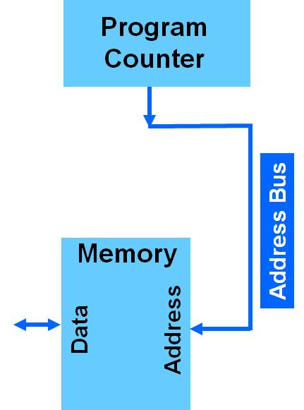
179 Simple Computer Big Picture We wish to apply this top-down, bottom-up methodology to the design of a simple 8-bit computer (or, microprocessor ) First step: Draw the big picture LED Output Port Switch Input Port Start Clock 180
180 Simple Computer Floor Plan Question: In the design of a computer, what is analogous to the floor plan of a house? The computer s programming model and instruction set Definition: The programming model of a computer is the set of user registers available to the programmer Definition: A collection of two or more flip-flops with a common clock (and generally a common purpose) is called a register In the simple computer designed here, the programming model will contain a single data register where the result accumulates (the accumulator, or A register for short), plus condition codes or flags (C, V, N, Z) 181
181 Simple Computer Floor Plan Definition: The instruction set of a computer is the set of operations the computer can be programmed to perform on data Instructions typically consist of several fields that indicate the operation to be performed ( operation code, or opcode) and the data on which the operation is to be performed (specified using an addressing mode) Our 8-bit computer will utilize a 3-bit opcode field (thus allowing 8 different kinds of instructions to be implemented) and a 5-bit address field (thus allowing 32 locations) 182
182 Simple Computer Floor Plan Instruction format: X X X Y Y Y Y Y XXX indicates operation to perform ( opcode ) YYYYY indicates location of operand ( address ) Called a two address machine since one operand will be the accumulator ( A ) register and the other operand will be obtained from the specified location in memory 183
183 Simple Computer Floor Plan Instruction set: Opcode Mnemonic Function Performed HLT Halt stop, discontinue execution LDA addr Load A with contents of location addr ADD addr Add contents of addr to contents of A SUB addr Subtract contents of addr from contents of A AND addr AND contents of addr with contents of A STA addr Store contents of A at location addr Note: We will use parentheses to denote the contents of a register or memory location, e.g., (A) is read as the contents of A 184
184 Simple Programming Example Addr Instruction Comments LDA Load A with contents of location ADD Add contents of location to A STA Store contents of A at location LDA Load A with contents of location AND AND contents of with contents of A STA Store contents of A at location LDA Load A with contents of location SUB Subtract contents of location from A STA Store contents of A at location HLT Stop discontinue execution 185
185 Location Contents Memory Snapshot Program Operands Results 186
186 Location Contents ADD Add: CF = 0 NF = 1 VF = 0 ZF = 0 187
187 Location Contents AND AND: CF = <unaffected> NF = 0 VF = <unaffected> ZF = 1 188
188 Location Contents CF = 1 NF = 0 VF = 1 ZF = 0 SUB Sub: ) Overflow! 189
189 Simple Computer Block Diagram Question: What functional blocks are necessary to implement a computer that executes a stored program consisting of the instructions we have just defined? Two basic steps are required to perform an instruction: (1) it must be fetched from memory, and (2) it must be decoded and executed 190
190 Simple Computer Block Diagram Functional blocks required: a place to store the program, operands, and computation results memory a way to keep track of which instruction is to be executed next program counter (PC) a place to temporarily stage an instruction while it is being executed instruction register (IR) a way to perform arithmetic and logic operations arithmetic logic unit (ALU) a way to coordinate and sequence the functions of the machine instruction decoder and micro-sequencer (IDMS) 191
191 Memory Address 192
192 Memory Address 193
193 Memory Address 194
194 Memory Address 195
195 Memory Address 196
196 Notes About Block Diagram Each functional block is self-contained (which means each block can be designed and tested independently) Additional instructions can be added by increasing the number of opcode bits Additional memory can be added by increasing the number of address bits The numeric range can be expanded by increasing the number of data bits 197
197 Clicker Quiz 198
198 Q1. The next instruction to fetch from memory is pointed to by the: A. accumulator B. program counter C. instruction register D. microsequencer E. none of the above 199
199 Q2. The place where an instruction fetched from memory is staged while it is being decoded and executed is the: A. accumulator B. program counter C. instruction register D. microsequencer E. none of the above 200
200 Q3. If two additional address bits were added to the Simple Computer, the number of memory locations the machine could access would increase: A. by two locations B. by four locations C. by two times the original number of locations D. by four times the original number of locations E. none of the above 201
201 Q4. The expression (10110) (A) + (10110) means: A. replace the contents of the accumulator with the sum of its current contents plus the contents of memory location B. replace the contents of the accumulator with the sum of its current contents plus the constant C. replace the contents of memory location with the sum of its current contents plus the contents of the accumulator D. add the constant to the contents of the accumulator and store the result in memory location E. none of the above 202
202 Purdue IM:PACT* Fall 2018 Edition *Instruction Matters: Purdue Academic Course Transformation Introduction to Digital System Design Module 4-H Simple Computer Instruction Execution Tracing
203 Reading Assignment: Meyer Supplemental Text, pp Learning Objectives: Trace the execution of a computer program, identifying each step of an instruction s microsequence (fetch and execute cycles) Distinguish between synchronous and combinational system control signals 204
204 Outline Review of top-down specification phase of design process Big picture Floor plan (instruction set) Block diagram Instruction execution tracing 205
205 Simple Computer Floor Plan Instruction set: Opcode Mnemonic Function Performed HLT Halt stop, discontinue execution LDA addr Load A with contents of location addr ADD addr Add contents of addr to contents of A SUB addr Subtract contents of addr from contents of A AND addr AND contents of addr with contents of A STA addr Store contents of A at location addr 206
206 Simple Computer Block Diagram Functional blocks required: a place to store the program, operands, and computation results memory a way to keep track of which instruction is to be executed next program counter (PC) a place to temporarily stage an instruction while it is being executed instruction register (IR) a way to perform arithmetic and logic operations arithmetic logic unit (ALU) a way to coordinate and sequence the functions of the machine instruction decoder and micro-sequencer (IDMS) 207
207 Memory Address 208
208 Simple Programming Example Addr Instruction Comments LDA Load A with contents of location ADD Add contents of location to A STA Store contents of A at location LDA Load A with contents of location AND AND contents of with contents of A STA Store contents of A at location LDA Load A with contents of location SUB Subtract contents of location from A STA Store contents of A at location HLT Stop discontinue execution 209

209
210
211
212

213
214
215
216
217 Notes About Instruction Tracing The clock edges drive the synchronous functions of the computer (e.g., increment program counter, load instruction register) The decoded states (here, fetch and execute) enable the combinational functions of the computer (e.g., turn on tristate buffers) 218
218 Purdue IM:PACT* Fall 2018 Edition *Instruction Matters: Purdue Academic Course Transformation Introduction to Digital System Design Module 4-I Simple Computer Bottom-Up Realization
219 Reading Assignment: Meyer Supplemental Text, pp Learning Objectives: Describe the operation of memory and the function of its control signals: MSL, MOE, and MWE Describe the operation of the program counter (PC) and the function of its control signals: ARS, PCC, and POA Describe the operation of the instruction register (IR) and the function of its control signals: IRL and IRA Describe the operation of the ALU and the function of its control signals: ALE, ALX, ALY, and AOE Describe the operation of the instruction decoder/microsequencer and derive the system control table Describe the basic hardware-imposed system timing constraints Discuss how the instruction register can be loaded with the contents of the memory location pointed to be the program counter and the program counter can be incremented on the same clock edge 220
220 Outline Bottom-up Realization Phase of Design Process Memory Program Counter Instruction Register Arithmetic Logic Unit Instruction Decoder and Microsequencer System Data Flow and Timing Analysis 221
221 Bottom-Up Implementation Having finished the top-down specification phase of the design process, we are now ready to implement each block identified from the bottom-up Note that, in practice, an important aspect of this process is to independently test (and debug) each block (or module) of the system as it is implemented If each module is independently tested and verified as it is implemented, then when the modules are assembled together into a system there is a much higher probability that it will work the first time! 222
222 Simple Computer Block Diagram Functional blocks required: a place to store the program, operands, and computation results memory a way to keep track of which instruction is to be executed next program counter (PC) a place to temporarily stage an instruction while it is being executed instruction register (IR) a way to perform arithmetic and logic operations arithmetic logic unit (ALU) a way to coordinate and sequence the functions of the machine instruction decoder and micro-sequencer (IDMS) 223
223 Read/Write Memory (RWM) Memory Address 224
224 Read/Write Memory (RWM) The name read/write memory (RWM) is given to memory arrays in which we can store and retrieve information at any time Most of the RWMs used in digital systems are randomaccess memories (RAMs), which means that the time it takes to read or write a bit of memory is independent of the bit s location in the RAM In a static RAM (SRAM), once data is written to a given location, it remains stored as long as power is applied to the chip If power is removed, data is lost this is referred to as a volatile memory 225
225 Read/Write Memory (RWM) An SRAM has three (typically active low) control inputs: a chip select (CS) signal that serves as the overall enable for the memory chip an output enable (OE) signal that tells the memory chip to drive the data output lines with the contents of the memory location specified on its address lines a write enable (WE) signal that tells the memory chip to write the data supplied on its data input lines at the memory location specified on its address lines 226
226 Read/Write Memory (RWM) SRAM normally has two access operations: READ: An address is placed on the address lines while CS and OE are asserted; the latch outputs for the selected location are output on the data lines WRITE: An address is placed on the address lines, data is placed on the data lines, then CS and WE are asserted; the latches of the selected location open, and the data is stored 227
227 Read/Write Memory (RWM) Each bit of memory (or SRAM cell) in a static RAM behaves as the circuit depicted below When the SEL input is asserted, the stored data is placed on the cell s output When both SEL and WR are asserted, the latch is open and a new data bit is stored SRAM cells are combined in an array with additional control logic to form a complete static RAM 228
228 Internal Structure of 8x4 SRAM 229
229 Read/Write Memory (RWM) Some things to note: during read operations, the output data is a combinational function of the address inputs, so no harm is done by changing the address while CS and OE are asserted during write operations, data is stored in latches this means that data must meet certain setup and hold times with respect to the negation of the WE signal also during write operations, the address lines must be stable for a certain setup time before WR is asserted internally and for a hold time after WR is negated 230
230 Read/Write Memory (RWM) Most SRAMs utilize a bi-directional data bus (i.e., the same data pins are used for reading and writing data) 231
231 Simple Computer Memory The memory for our simple computer will contain 32 locations (5-bit address), each 8 bits wide (i.e., a 32x8 memory) The memory subsystem will have three control signals: MSL: Memory SeLect MOE: Memory Output Enable MWE: Memory Write Enable NOTE: For simplicity (and clarity) all system control signals as well as address and data bus signals will be assumed to be ACTIVE HIGH 232
232 Clicker Quiz 233
233 Q1. When a set of control signals are said to be mutually exclusive, it means that: A. all the control signals may be asserted simultaneously B. only one control signal may be asserted at a given instant C. each control signal is dependent on the others D. any combination of control signals may be asserted at a given instant E. none of the above 234
234 Q2. For the memory subsystem, the set of signals that are mutually exclusive is: A. MSL and MOE B. MSL and MWE C. MOE and MWE D. MSL, MOE, and MWE E. none of the above 235
235 Simple Computer Block Diagram Functional blocks required: a place to store the program, operands, and computation results memory a way to keep track of which instruction is to be executed next program counter (PC) a place to temporarily stage an instruction while it is being executed instruction register (IR) a way to perform arithmetic and logic operations arithmetic logic unit (ALU) a way to coordinate and sequence the functions of the machine instruction decoder and micro-sequencer (IDMS) 236
236 Memory Address 237
237 Program Counter The program counter (PC) is basically a binary up counter with tri-state outputs The functions and corresponding control signals required are as follows: ARS: Asynchronous ReSet PCC: Program Counter Count enable POA: Program counter Output on Address bus tri-state buffer enable 238
238 /* Program Counter Module */ module pc(clk, PCC, POA, RST, ADRBUS_z); input wire CLK; input wire PCC; // PC count enable input wire POA; // PC output on address bus tri-state enable input wire RST; // asynchronous reset (connected to START) output wire [4:0] ADRBUS_z; wire [4:0] next_pc; reg [4:0] PC; assign ADRBUS_z = POA? PC : 5'bZZZZZ; (posedge CLK, posedge RST) begin if (RST == 1'b1) PC <= 5'b00000; else PC <= next_pc; end // (PCC)? count up : retain value; assign next_pc = (PCC)? (PC+1) : PC; endmodule 239
239 Simple Computer Block Diagram Functional blocks required: a place to store the program, operands, and computation results memory a way to keep track of which instruction is to be executed next program counter (PC) a place to temporarily stage an instruction while it is being executed instruction register (IR) a way to perform arithmetic and logic operations arithmetic logic unit (ALU) a way to coordinate and sequence the functions of the machine instruction decoder and micro-sequencer (IDMS) 240
240 241
241 Instruction Register The instruction register (IR) is basically an 8-bit data register, with tri-state outputs on the lower 5 bits Note that the upper 3 bits (opcode field) are output directly to the instruction decoder and microsequencer The functions and corresponding control signals required are as follows: IRL: Instruction Register Load enable IRA: Instruction Register Address field tri-state output enable 242
242 /* Instruction Register Module */ module ir(clk, IR_z, DB_z, IRL, IRA); input wire CLK; input wire IRL; // IR load enable input wire IRA; // IR output on address bus enable input wire [7:0] DB_z; // data bus output wire [7:0] IR_z; // IR_z[4]..IR_z[0] connected to address bus // IR_z[7]..IR_z[5] supply opcode to IDMS reg [7:0] IR; wire [7:0] next_ir; assign IR_z[4:0] = IRA? IR[4:0] : 5'bZZZZZ; assign IR_z[7:5] = IR[7:5]; (posedge CLK) begin IR <= next_ir; end // (IRL)? load : retain state (select load or retain state based on IRL) assign next_ir = (IRL)? DB_z : IR; endmodule 243
243 Simple Computer Block Diagram Functional blocks required: a place to store the program, operands, and computation results memory a way to keep track of which instruction is to be executed next program counter (PC) a place to temporarily stage an instruction while it is being executed instruction register (IR) a way to perform arithmetic and logic operations arithmetic logic unit (ALU) a way to coordinate and sequence the functions of the machine instruction decoder and micro-sequencer (IDMS) 244
244 245
245 Arithmetic Logic Unit The arithmetic logic unit (ALU) is a multi-function register that performs all the arithmetic and logical (Boolean) operations necessary to implement the instruction set The functions and corresponding control signals required are as follows: ALE: ALU Enable ALX: ALU X function select ALY: ALU Y function select AOE: A register tri-state Output Enable 246
246 /* ALU Module */ module alu(clk, ALE, AOE, ALX, ALY, DB_z, CF, VF, NF, ZF); /* 8-bit, 4-function ALU with bi-directional data bus Accumulator register is AQ, tri-state data bus is DB_z ADD: (AQ[7:0]) <- (AQ[7:0]) + DB_z[7:0] SUB: (AQ[7:0]) <- (AQ[7:0]) DB_z[7:0] LDA: (AQ[7:0]) <- DB_z[7:0] AND: (AQ[7:0]) <- (AQ[7:0]) & DB_z[7:0] OUT: Value in AQ[7:0] output on data bus DB_z[7:0] AOE ALE ALX ALY Function CF ZF NF VF === === === === ======== == == == == ADD X X X X SUB X X X X LDA X X AND X X 1 0 d d OUT 0 0 d d <none> X -> flag affected -> flag not affected Note: If ALE = 0, the state of all register bits should be retained */ 247
![ALU Multiplexer Block Diagram (Bit i) If ALX=1, then ALY selects LDA (ALY=0) or AND (ALY=1) If ALX=0, then ALY selects ADD (ALY=0) or SUB (ALY=1) L[i] S[i] CY[i] CY[i-1] The LSB Cin CY[i-1] is](/docs-images/86/93688669/images/247-1.jpg "connected to ALY: 0 for ADD, 1 for SUB (to obtain the radix complement of the subtrahend) ALX selects ADD/SUB (ALX=0) or LDA/AND (ALX=1) AQ[i] DB_z[i] ALE controls A register retaining state (ALE=0)")
247 ALU Multiplexer Block Diagram (Bit i) If ALX=1, then ALY selects LDA (ALY=0) or AND (ALY=1) If ALX=0, then ALY selects ADD (ALY=0) or SUB (ALY=1) L[i] S[i] CY[i] CY[i-1] The LSB Cin CY[i-1] is connected to ALY: 0 for ADD, 1 for SUB (to obtain the radix complement of the subtrahend) ALX selects ADD/SUB (ALX=0) or LDA/AND (ALX=1) AQ[i] DB_z[i] ALE controls A register retaining state (ALE=0) or taking on new state (ALE=1) ALU[i] is the next state of AQ[i] (the A register) ALU[i] 248
248 input wire CLK; // ALU control lines input wire ALE; input wire AOE; input wire ALX, ALY; inout wire [7:0] DB_z; output reg CF, VF, NF, ZF; // Carry equations wire [7:0] CY; // overall ALU enable // data bus tri-state output enable // function select // bidirectional 8-bit tri-state data bus // condition code register bits (flags) // Carry, Overflow, Negative, Zero // Combinational ALU outputs wire [7:0] ALU; wire [7:0] S; wire [7:0] L; reg [7:0] AQ; // Adder/subtractor sum // LDA/AND multiplexer output // A register flip-flops // Next state variables reg next_cf, next_vf, next_nf, next_zf; reg [7:0] next_aq; 249
249 // Declaration of intermediate equations // Least significant bit carry in (0 for ADD, 1 for SUB => ALY) assign CIN = ALY; // Intermediate equations for adder/subtractor SUM (S) selected when ALX = 0 assign S = AQ ^ (DB_z ^ ALY) ^ {CY[6:0],CIN}; // Ripple carry equations (CY[7] is COUT, DB_z is data from data bus) assign CY = AQ & (ALY ^ DB_z) AQ & {CY[6:0],CIN} ALY & DB_z & {CY[6:0],CIN}; // Intermediate equations for LOAD and AND, selected when ALX = 1 // (ALY)? AND : LDA (select LDA or AND based on ALY) assign L = ALY? AQ & DB_z : DB_z ; // Combinational ALU outputs // (ALX)? L : S (select LDA/AND or ADD/SUB based on ALX) assign ALU = ALX? L : S; 250
250 // Register bit and data bus control equations CLK) begin AQ <= next_aq; end (AQ, ALE, ALU) begin next_aq = ALE? ALU : AQ; end assign DB_z = AOE? AQ : 8'bZZZZZZZZ; // Condition code register state equations (posedge CLK) begin CF <= next_cf; ZF <= next_zf; NF <= next_nf; VF <= next_vf; end (CF, NF, ZF, VF, ALE, ALX, ALY, CY) begin next_cf = ALE? (ALX? CF : (CY[7]) : CF; next_zf = ALE? (ALU == 8 b ) : ZF; next_nf = ALE? ALU[7] : NF; next_vf = ALE? (ALX? VF : (CY[7] ^ CY[6])) : VF; end endmodule 251
251 Clicker Quiz 252
252 Block Diagram for Bit 3 of a Simple Computer ALU Qi-1 Q2 Q1 Q0 Q0 ALY ALY i 0 A1 A0 2:1 mux F X Y Full Adder Cin Cout S C 3 C 2 Assume LSB Cin is connected to ALY ALX i 0 A1 A0 2:1 mux F D Q Q3 AOE DB 3 CLOCK ALE i 0 A1 A0 2:1 mux F 253
253 Q1. If the input control combination AOE=0, ALE=1, ALX=0, ALY=0 is applied to this circuit, the function performed will be: A. ADD B. SUBTRACT C. LOAD D. NEGATE E. none of the above 254
254 Q2. If the input control combination AOE=0, ALE=1, ALX=1, ALY=0 is applied to this circuit, the function performed will be: A. ADD B. SUBTRACT C. LOAD D. NEGATE E. none of the above 255
255 Simple Computer Block Diagram Functional blocks required: a place to store the program, operands, and computation results memory a way to keep track of which instruction is to be executed next program counter (PC) a place to temporarily stage an instruction while it is being executed instruction register (IR) a way to perform arithmetic and logic operations arithmetic logic unit (ALU) a way to coordinate and sequence the functions of the machine instruction decoder and micro-sequencer (IDMS) 256
256 Memory Address 257
257 Instruction Decoder and Microsequencer The instruction decoder and microsequencer (IDMS) is a state machine that orchestrates the activity of all the other functional blocks There are two basic steps involved in processing each instruction of a program (called a micro-sequence): fetching the instruction from memory (at the location pointed to by the PC), loading it into the IR, and incrementing the PC executing the instruction staged in the IR based on the opcode field and the operand address field 258
258 Instruction Decoder and Microsequencer Since there are only two states (fetch and execute), a single flip-flop can be used to implement the state counter ( SQ ) The control signals that need to be asserted during the fetch cycle include: POA: turn on PC output buffers MSL: select memory MOE: turn on memory output buffers IRL: enable IR load PCC: enable PC count NOTE: The synchronous functions (IRL and PCC) will take place on the clock edge that causes the state counter to transition from the FETCH state to the EXECUTE state 259

259 Instruction Decoder and Microsequencer The control signals that need to be asserted during an execute cycle for the synchronous ALU functions (ADD, SUB, LDA, AND) are: IRA: turn on operand address output buffers MSL: select memory MOE: turn on memory data output buffers ALE: enable ALU operation ALX, ALY: select ALU function The control signals that need to be asserted during an execute cycle for STA are: IRA: turn on operand address output buffers MSL: select memory MWE: enable memory write AOE: turn on A register output buffers 260

260 Decoded State System Control Signals Instruction Mnemonic MSL MOE MWE PCC POA IRL S0 H H H H H IRA AOE S1 HLT L L L L S1 LDA addr H H H H H S1 ADD addr H H H H S1 SUB addr H H H H H S1 AND addr H H H H H H S1 STA addr H H H H ALE ALX ALY 261
261 Instruction Decoder and Microsequencer In order to stop execution (i.e., disable all the functional blocks) when a HLT instruction is executed, an additional flip-flop will be used (called RUN ), as follows: when the START pushbutton is pressed, the RUN flipflop will be asynchronously set when a HLT instruction is executed, the RUN flip-flop will be asynchronously cleared the RUN signal will be ANDed with the synchronous system enable signals, thus effectively halting execution when a HLT instruction is executed 262
262 /* Instruction Decoder and Microsequencer */ module idms(clk, START, OP, MSL, MOE, MWE, PCC, POA, ARS, IRL, IRA, ALE, ALX, ALY, AOE); input wire CLK; input wire START; input wire [2:0] OP; output wire MSL, MOE, MWE; output wire PCC, POA, ARS; output wire IRL, IRA; output wire ALE, ALX, ALY, AOE; reg SQ, next_sq; reg RUN, next_run; wire LDA, STA, ADD, SUB, AND, HLT; wire [1:0] S; wire RUN_ar; // Asynchronous START pushbutton // opcode bits (input from IR5..IR7) // Memory control signals // PC control signals // IR control signals // ALU control signals (without flags) // State counter // RUN/HLT state // Opcode names // State variables // Asynchronous reset for RUN 263

263 assign HLT = ~OP2 & ~OP1 & ~OP0; // HLT opcode = 000 assign LDA = ~OP2 & ~OP1 & OP0; // LDA opcode = 001 assign ADD = ~OP2 & OP1 & ~OP0; // ADD opcode = 010 assign SUB = ~OP2 & OP1 & OP0; // SUB opcode = 011 assign AND = OP2 & ~OP1 & ~OP0; // AND opcode = 100 assign STA = OP2 & ~OP1 & OP0; // STA opcode = 101 // Decoded state definitions assign S[0] = ~SQ; // fetch assign S[1] = SQ; // execute // State counter (posedge CLK, posedge START) begin if(start == 1'b1) // start in fetch state SQ <= 1'b0; else // if RUN negated, resets SQ SQ <= next_sq; end (SQ, RUN) begin next_sq = RUN & ~SQ end // Run/stop assign RUN_ar = S[1] & HLT; (posedge CLK, posedge RUN_ar, posedge START) begin if(start == 1'b1) // RUN set to 1 when START asserted RUN <= 1'b1; else if(run_ar == 1'b1) // RUN is cleared when HLT is executed RUN <= 1'b0; A D flip-flop synthesized by an always block will retain its value by default unless otherwise specified end 264
![// System control equations assign MSL = RUN & (S[0] S[1] & (LDA STA ADD SUB AND)); assign MOE = S[0] S[1] & (LDA ADD SUB AND); assign MWE = S[1] & STA; assign ARS = START; assign PCC = RUN & S[0];](/docs-images/86/93688669/images/264-0.jpg "assign POA = S[0]; assign IRL = RUN & S[0]; assign IRA = S[1] & (LDA STA ADD SUB AND); assign AOE = S[1] & STA; assign ALE = RUN & S[1] & (LDA ADD SUB AND); assign ALX = S[1] & (LDA AND); assign ALY")
264 // System control equations assign MSL = RUN & (S[0] S[1] & (LDA STA ADD SUB AND)); assign MOE = S[0] S[1] & (LDA ADD SUB AND); assign MWE = S[1] & STA; assign ARS = START; assign PCC = RUN & S[0]; assign POA = S[0]; assign IRL = RUN & S[0]; assign IRA = S[1] & (LDA STA ADD SUB AND); assign AOE = S[1] & STA; assign ALE = RUN & S[1] & (LDA ADD SUB AND); assign ALX = S[1] & (LDA AND); assign ALY = S[1] & (SUB AND); endmodule 265
265 System Data Flow and Timing Analysis General procedure Understand operation of individual functional units Memory Program counter Instruction register Arithmetic logic unit Instruction decoder and microsequencer (New functional blocks to be added) 266
266 System Data Flow and Timing Analysis General procedure Understand function ( data processing ) performed by each instruction Identify address and data flow required to execute each instruction Identify micro-operations required to execute each instruction Identify control signals that need to be asserted to generate the required sequence of micro-operations for each instruction Examine timing relationship of control signals 267
267 System Data Flow and Timing Analysis Basic hardware-imposed constraints Only one device is allowed to drive a bus during any machine cycle (i.e., bus fighting must be avoided) Data cannot pass through more than one (edge-triggered) flip-flop or latch per cycle 268

268 Memory Address 269

269
270 Clicker Quiz 271
271 Q1. The increment of the program counter (PC) needs to occur as part of the fetch cycle because: A. if it occurred on the execute cycle, the new value might not be stable in time for the subsequent fetch cycle B. if it occurred on the execute cycle, it would not be possible to execute an STA instruction C. if it occurred on the execute cycle, it would not be possible to read an operand from memory D. if it occurred on the execute cycle, it would not be possible to read an instruction from memory E. none of the above 272
272 Q2. The program counter (PC) can be incremented on the same cycle that its value is used to fetch an instruction from memory because: A. the synchronous actions associated with the IRL and PCC control signals occur on different fetch cycle phases B. the IRL and PCC control signals are not asserted simultaneously by the IDMS C. the load of the instruction register is based on the data bus value prior to the system CLOCK edge, while the increment of the PC occurs after the CLOCK edge D. the load of the instruction register occurs on the negative CLOCK edge, while the increment of the PC occurs on the positive CLOCK edge E. none of the above 273
273 Q3. Incrementing the program counter (PC) on the same clock edge that loads the instruction register (IR) does not cause a problem because: A. the memory will ignore the new address the PC places on the address bus B. the output buffers in the PC will not allow the new PC value to affect the address bus until the next fetch cycle C. the IR will be loaded with the value on the data bus prior to the clock edge while the contents of the PC will increment after the clock edge D. the value in the PC will change in time for the correct value to be output on the address bus (and fetch the correct instruction), before the IR load occurs E. none of the above 274
274 Q4. The hardware constraint that data cannot pass through more than one edge-triggered flip-flop per clock cycle is based on the fact that: A. only a single entity can drive a bus on a given clock cycle B. the system clock has limited driving capability C. the flip-flops that comprise a register do not change state simultaneously, so additional time must be provided before the register s output can be used D. for a D flip-flop with clocking period, Q(t+ )=D(t) E. none of the above 275
275 Purdue IM:PACT* Fall 2018 Edition *Instruction Matters: Purdue Academic Course Transformation Introduction to Digital System Design Module 4-J Simple Computer Basic Extensions
276 Reading Assignment: Meyer Supplemental Text, pp Learning Objectives: Modify a reference ALU design to perform different functions (e.g., shift and rotate) Describe how input/output (IN/OUT) instructions can be added to the base machine architecture Describe the operation of the I/O block and the function of its control signals: IOR and IOW Compare and contrast the operation of OUT instructions with and without a transparent latch as an integral part of the I/O block Compare and contrast jump and branch transfer-of-control instructions along with the architectural features needed to support them Distinguish between conditional and unconditional branches Describe the basis for which a conditional branch is taken or not taken 277
277 Outline Overview Adding shift instructions Adding input/output (I/O) instructions Adding transfer of control instructions 278
278 Overview We will use the two available opcodes (110 and 111) to add new instructions to the basic machine, a pair at a time Opcode Mnemonic Function Performed HLT Halt stop, discontinue execution LDA addr Load A with contents of location addr ADD addr Add contents of addr to contents of A SUB addr Subtract contents of addr from contents of A AND addr AND contents of addr with contents of A STA addr Store contents of A at location addr
279 Overview We will add rows to the system control table to add the new instructions and add columns to add new control signals Decoded State Instruction Mnemonic MSL MOE MWE PCC POA IRL S0 H H H H H S1 HLT L L L L S1 LDA addr H H H H H S1 ADD addr H H H H S1 SUB addr H H H H H S1 AND addr H H H H H H IRA S1 STA addr H H H H S1 S1 AOE ALE ALX ALY 280
280 Adding Shift Instructions Definition: A shift instruction translates the bits in a register (here, the A register) one place to the left or to the right Definition: An end off shift discards the bit that gets shifted out Definition: A preserving shift retains the bit shifted out (typically in the CF condition code bit) Definition: A logical shift is a zero fill shift Definition: An arithmetic shift is a sign preserving shift (i.e., the sign bit gets replicated as the data is shifted right) 281
281 Shift Instruction Examples Given: (A) = After logical shift left: CF=1 After logical shift right: CF=0 After arithmetic shift left: CF=1 After arithmetic shift right: CF=0 Note: An arithmetic left shift is identical to a logical left shift 282
282 Adding Shift Instructions Modify the ALU to function as follows: ALX ALY Function Performed 0 0 Load 0 1 Logical Shift Right 1 0 Arithmetic/Logical Shift Left 1 1 Arithmetic Shift Right The CF condition code bit can be used to preserve the bit that gets shifted out 283
283 Modified Instruction Set Opcode Mnemonic Function Performed HLT Halt stop, discontinue execution LDA addr Load A with contents of location addr LSR Logically shift contents of A right ASL Arithmetically/Logically shift contents of A left ASR Arithmetically shift contents of A right STA addr Store contents of A at location addr
284 Modified System Control Table Decoded State Instruction Mnemonic MSL MOE MWE PCC POA IRL S0 H H H H H S1 HLT L L L L S1 LDA addr H H H H S1 LSR H H S1 ASL H H S1 ASR H H H IRA S1 STA addr H H H H S1 S1 AOE ALE ALX ALY 285
285 /* ALU Module Version 2 */ module alu(clk, ALE, AOE, ALX, ALY, DB, CF, VF, NF, ZF); /* 8-bit, 4-function ALU with bi-directional data bus LDA: (AQ[7:0]) <- DB_z[7:0] LSR: (AQ[7:0]) <- 0 AQ7 AQ6 AQ5 AQ4 AQ3 AQ2 AQ1, CF <- AQ0 ASL: (AQ[7:0]) <- AQ6 AQ5 AQ4 AQ3 AQ2 AQ1 AQ0 0, CF <- AQ7 ASR: (AQ[7:0]) <- AQ7 AQ7 AQ6 AQ5 AQ4 AQ3 AQ2 AQ1, CF <- AQ0 OUT: Value in AQ[7:0] output on data bus DB_z[7:0] AOE ALE ALX ALY Function CF ZF NF VF === === === === ======== == == == == LDA X X LSR X X X ASL X X X ASR X X X 1 0 d d OUT 0 0 d d <none> X -> flag affected -> flag not affected Note: If ALE = 0, the state of all register bits should be retained */ 286
286 input wire CLK; // ALU control lines input wire ALE; input wire AOE; input wire ALX, ALY; inout wire [7:0] DB_z; output reg CF, VF, NF, ZF; // Overall ALU enable // Data bus tri-state output enable // Function select // Bidirectional 8-bit data bus // Condition code bits (flags) // Carry, Overflow, Negative, Zero // Combinational ALU outputs wire [7:0] ALU; // Accumulator (A) register reg [7:0] AQ; // Next state variables reg next_cf, next_vf, next_nf, next_zf; reg [7:0] next_aq; 287
287 // Combinational ALU outputs (ALX, ALY, DB_z) begin case ({ALX,ALY}) 2'b00: ALU = DB_z; 2'b01: ALU = {1'b0,AQ[7:1]}; 2'b10: ALU = {AQ[6:0],1'b0}; 2'b11: ALU = {AQ[7],AQ[7:1]}; endcase end // LDA // LSR // ASL // ASR // Register bit and data bus control equations CLK) begin AQ <= next_aq; end (ALE, ALU, AQ) begin next_aq = ALE? ALU : AQ; end assign DB_z = AOE? AQ : 8'bZZZZZZZZ; 288
288 // Flag register state equations (posedge CLK) begin CF <= next_cf; ZF <= next_zf; NF <= next_nf; VF <= next_vf; end (ALE, ALX, ALY, CF, ZF, NF, VF, ALU, AQ) begin casez ({ALE,ALX,ALY}) 3'b0??: next_cf = 1'b0; 3'b100: next_cf = CF; // LDA (not affected) 3'b101: next_cf = AQ[0]; // LSR 3'b110: next_cf = AQ[7]; // ASL 3'b111: next_cf = AQ[0]; // ASR endcase next_zf = ALE? (ALU == 8 b ) : ZF; next_nf = ALE? ALU[7] : NF; next_vf = VF; // NOTE: NOT AFFECTED end endmodule 289
289 Clicker Quiz 290
290 Block Diagram for Bit 3 of a Simple Computer ALU Qi-1 Q2 Q1 Q0 Q0 ALY ALY i 0 A1 A0 2:1 mux F X Y Full Adder Cin Cout S C 3 C 2 Assume LSB Cin is connected to ALY ALX i 0 A1 A0 2:1 mux F D Q Q3 AOE DB 3 CLOCK ALE i 0 A1 A0 2:1 mux F 291
291 Q1. If the input control combination AOE=1, ALE=1, ALX=1, ALY=1 is applied to this circuit, the function (inadvertently) performed on (A) will be equivalent to: A. logical left shift B. logical right shift C. rotate left D. rotate right E. none of the above 292
292 Adding I/O Instructions When we first drew the big picture of our simple computer, we included a switch input port and an LED output port LED Output Port Switch Input Port Start Clock 293

293
294 Adding I/O Instructions Need two new instructions: IN addr input data from port addr and load into the A register OUT addr output data in A register to port addr Here, the address field of the instruction is used to specify a port address (or, I/O device ID) Also need two new control signals: IOR asserted when IN ( I/O read ) occurs IOW asserted when OUT ( I/O write ) occurs 295
295 /* Input/Output Port */ module io(adrbus_z, IN, OUT, IOR, IOW, DB_z); input wire [4:0] ADRBUS_z; input wire [7:0] IN; input wire IOR; input wire IOW; output wire [7:0] OUT; inout wire [7:0] DB_z; // address bus // input port // input port read // input port write // output port // bidirectional data bus wire PS; // Port select equation for port address assign PS = (ADRBUS_z == 5 b00000); assign DB_z = IOR & PS? IN assign OUT = IOW & PS? DB_z endmodule : 8'bZZZZZZZZ; : 8'bZZZZZZZZ; Issue: Output port bits are valid only as long as IOW&PS is asserted (Hi-Z otherwise) 296
296 /* Input/Output Port with Output Latch */ module io(adrbus_z, IN, OUT, IOR, IOW, DB_z); input wire [4:0] ADRBUS_z; input wire [7:0] IN; input wire IOR; input wire IOW; output wire [7:0] OUT; inout wire [7:0] DB_z; wire PS; // address bus // input port // input port read // input port write // output port // bidirectional data bus // Port select equation for port address assign PS = (ADRBUS_z == 5 b00000); assign DB_z = IOR & PS? IN : 8'bZZZZZZZZ; // Transparent latch for output port (IOW, PS, DB_z) begin if((iow & PS) == 1 b1) OUT = DB_z; end The if construct without an else creates an inferred latch endmodule 297
297 Adding I/O Instructions Modified system control table: Decoded State Instruction Mnemonic MSL MOE MWE PCC POA IRL S0 H H H H H S1 HLT L L L L S1 LDA addr H H H H H S1 ADD addr H H H H S1 SUB addr H H H H H S1 AND addr H H H H H H IRA S1 STA addr H H H H S1 IN port H H H H S1 OUT port H H H AOE ALE ALX ALY IOR IOW Equations that need to be updated: IRA, AOE, ALE, ALX Equations that need to be added: IOR, IOW 298
![// System control equations assign MSL = RUN & (S[0] S[1] & (LDA STA ADD SUB AND)); assign MOE = S[0] S[1] & (LDA ADD SUB AND); assign MWE = S[1] & STA; assign ARS = START; assign PCC = RUN & S[0];](/docs-images/86/93688669/images/298-0.jpg "assign POA = S[0]; assign IRL = RUN & S[0]; assign IRA = S[1] & (LDA STA ADD SUB AND IN OUT); assign AOE = S[1] & (STA OUT); assign ALE = RUN & S[1] & (LDA ADD SUB AND IN); assign ALX = S[1] & (LDA")
298 // System control equations assign MSL = RUN & (S[0] S[1] & (LDA STA ADD SUB AND)); assign MOE = S[0] S[1] & (LDA ADD SUB AND); assign MWE = S[1] & STA; assign ARS = START; assign PCC = RUN & S[0]; assign POA = S[0]; assign IRL = RUN & S[0]; assign IRA = S[1] & (LDA STA ADD SUB AND IN OUT); assign AOE = S[1] & (STA OUT); assign ALE = RUN & S[1] & (LDA ADD SUB AND IN); assign ALX = S[1] & (LDA AND); assign ALY = S[1] & (SUB AND); assign IOR = S[1] & IN; assign IOW = S[1] & OUT; endmodule 299
299 Clicker Quiz 300
300 Q1. If the output port pins are latched, data written to the port will remain on its pins: A. only during the execute cycle of the OUT instruction B. only when the clock signal is high C. until another OUT instruction writes different data to the port D. until the next instruction is executed E. none of the above 301
301 Q2. If the output port pins are not latched, data written to the port will remain on its pins: A. only during the execute cycle of the OUT instruction B. only when the clock signal is high C. until another OUT instruction writes different data to the port D. until the next instruction is executed E. none of the above 302
302 Adding Transfer of Control Instructions There are two basic types of transfer-of-control instructions: absolute: the operand field contains the address in memory at which execution should continue ( jump ) relative: the operand field contains the signed offset that should be added to the PC to determine the location at which execution should continue ( branch ) Jumps or branches can be unconditional ( always happen ) or conditional ( happen only when a specified condition is met which is usually a function of the condition codes) 303
303 Adding Transfer of Control Instructions For the purpose of illustration, we will add an unconditional jump ( JMP ) instruction to our simple computer along with a single conditional jump ( Jcond ) The conditional jump illustrated will be a jump if ZF set ( JZF ) instruction To execute a jump instruction, the operand field (from the IR) will be loaded into the PC via the address bus when PLA is asserted Note that, for the conditional jump instruction, that if the condition is not met, the execute cycle will be a no-operation (or, NOP ) cycle 304
304 305
305 /* Modified Program Counter with Load Capability */ module pc(clk, PCC, POA, ADRBUS_z, PLA, RST); input wire CLK; input wire PCC; input wire POA; input wire PLA; input wire RST; // PC count enable // PC output on address bus tri-state enable // PC load from address bus enable // Asynchronous reset (connected to START) inout wire [4:0] ADRBUS_z; // address bus // NOTE: Assume PCC and PLA are mutually exclusive reg [4:0] PC, next_pc; assign ADRBUS_z = POA? PC : 5'bZZZZZ; (posedge CLK, posedge RST) begin if (RST == 1'b1) PC <= 5'b00000; else PC <= next_pc; end (PCC, PC) begin if (PLA == 1 b1) // load next_pc = ADRBUS_z; else if (PCC == 1 b1) // count up by 1 next_pc = PC + 1; else // retain state next_pc = PC; end endmodule 306
306 Adding Transfer of Control Instructions Modified system control table: Decoded State Instruction Mnemonic MSL Equation that needs to be updated: IRA Equation that needs to be added: PLA MOE MWE PCC POA IRL S0 H H H H H S1 HLT L L L L S1 LDA addr H H H H H S1 ADD addr H H H H S1 SUB addr H H H H H S1 AND addr H H H H H H IRA S1 STA addr H H H H S1 JMP addr H H S1 JZF addr ZF ZF AOE ALE ALX ALY PLA 307
![// System control equations assign MSL = RUN & (S[0] S[1] & (LDA STA ADD SUB AND)); assign MOE = S[0] S[1] & (LDA ADD SUB AND); assign MWE = S[1] & STA; assign ARS = START; assign PCC = RUN & S[0];](/docs-images/86/93688669/images/307-0.jpg "assign POA = S[0]; assign IRL = RUN & S[0]; assign IRA = S[1] & (LDA STA ADD SUB AND JMP JZF&ZF); assign AOE = S[1] & STA; assign ALE = RUN & S[1] & (LDA ADD SUB AND); assign ALX = S[1] & (LDA AND);")
307 // System control equations assign MSL = RUN & (S[0] S[1] & (LDA STA ADD SUB AND)); assign MOE = S[0] S[1] & (LDA ADD SUB AND); assign MWE = S[1] & STA; assign ARS = START; assign PCC = RUN & S[0]; assign POA = S[0]; assign IRL = RUN & S[0]; assign IRA = S[1] & (LDA STA ADD SUB AND JMP JZF&ZF); assign AOE = S[1] & STA; assign ALE = RUN & S[1] & (LDA ADD SUB AND); assign ALX = S[1] & (LDA AND); assign ALY = S[1] & (SUB AND); assign PLA = S[1] & (JMP JZF & ZF); endmodule
308 Clicker Quiz 309
309 Q1. Implementation of branch instructions (that perform a relative transfer of control) requires the following modification to the program counter: A. add a bi-directional path to the data bus B. use the ALU to compute the address of the next instruction C. make it an up/down counter D. add a two s complement N-bit adder circuit (where N is the address bus width) E. none of the above 310
310 Q2. Whether or not a conditional branch is taken or not taken depends on: A. the value of the program counter B. the state of the condition code bits C. the cycle of the state counter D. the value in the accumulator E. none of the above 311
311 Thought Questions What would be required to add a jump if less than ( JLT ) or a jump if greater than or equal to ( JGE ) instruction? A 1 A 0 (A) B 1 B 0 (B)? C Z N V (A) = (B) (A) < (B) (A) > (B) (A) > (B) (A) > (B) (A) = (B) (A) > (B) (A) > (B) (A) < (B) (A) < (B) (A) = (B) (A) < (B) (A) < (B) (A) < (B) (A) > (B) (A) = (B) These jump conditions can be determined based on the ALU flags (N, C, Z, V) JLT condition = N V + N V = N V JGE condition = JLT = (N V) 312
312 Thought Questions How could a compare ( CMP ) instruction be implemented? How is this different than a subtract ( SUB )? A CMP works the same as SUB except that the result of (A) (addr) is not stored in the A register (i.e., only the flags are affected) 313
313 Purdue IM:PACT* Fall 2018 Edition *Instruction Matters: Purdue Academic Course Transformation Introduction to Digital System Design Module 4-K Simple Computer Advanced Extensions
314 Reading Assignment: Meyer Supplemental Text, pp Learning Objectives: describe the changes needed to the instruction decoder/microsequencer in order to dynamically change the number of instruction execute cycles based on the opcode compare and contrast the machine s asynchronous reset ( START ) with the synchronous state counter reset ( RST ) describe the operation of a stack mechanism (LIFO queue) describe the operation of the stack pointer (SP) register and the function of its control signals: ARS, SPI, SPD, SPA compare and contrast the two possible stack conventions: SP pointing to the top stack item vs. SP pointing to the top stack item describe how stack manipulation instructions (PSH/POP) can be added to the base machine architecture discuss the consequences of having an unbalanced set of PSH and POP instructions in a given program 315
315 Reading Assignment: Meyer Supplemental Text, pp Learning Objectives, continued: discuss the reasons for using a stack as a subroutine linkage mechanism: arbitrary nesting of subroutine calls, passing parameters to subroutines, recursion, and reentrancy describe how subroutine linkage instructions (JSR/RTS) can be added to the base machine architecture analyze the effect of changing the stack convention utilized (SP points to top stack item vs. next available location) on instruction cycle counts 316
316 Outline Modifications to state counter and instruction decoder to accommodate instructions with multiple execute cycles Introduction of a stack mechanism Use of a stack to implement push (PSH) and pop (POP) instructions Identification of micro-operations that can be overlapped Modifications to the system architecture necessary to implement subroutine linkage instructions Implementation of subroutine call (JSR) and return (RTS) instructions 317
317 State Counter Modifications All of the simple computer instructions discussed thus far have required only two states: a fetch cycle followed by a single execute cycle Many real world instructions require more than a single execute state to achieve their desired functionality We wish to extend the state counter (and the instruction decoder) to accommodate instructions that require multiple execute cycles (here, up to three) 318
318 State Counter Modifications In the process of adding this capability, we want to make sure our original shorter instructions do not incur a penalty (i.e., execute slower) To accomplish this, we need to design the state counter so that the number of execute cycles can be dynamically changed based on the opcode of the instruction being executed To provide up to three execute cycles, we will replace the state counter flip-flop with a two-bit binary counter that has a synchronous reset input (in addition to an asynchronous clear) 319
319 State Counter Modifications The state names will now be: S0 (fetch) S1 (first execute) S2 (second execute) S3 (third execute) We will also add a new system control signal RST (connected to the synchronous reset of the binary counter) that will be asserted on the last execute state of each instruction, thereby synchronously resetting the state counter to zero (so that the next cycle will be a fetch ) 320
320 /* Instruction Decoder and Microsequencer with Multi-Execution States */ module idmsr(clk, START, OP, MSL, MOE, MWE, PCC, POA, ARS, IRL, IRA, ALE, ALX, ALY, AOE); input wire CLK; input wire START; input wire [2:0] OP; output wire MSL, MOE, MWE; output wire PCC, POA, ARS; output wire IRL, IRA; output wire ALE, ALX, ALY, AOE; // Asynchronous START pushbutton // opcode bits (input from IR5..IR7) // Memory control signals // PC control signals // IR control signals // ALU control signals reg SQA, SQB; reg RUN; wire RST; // State counter low bit, high bit // RUN/HLT state // Synchronous state counter reset wire LDA, STA, ADD, SUB, AND, HLT; wire [3:0] S; reg next_sqa, next_sqb; wire RUN_ar; // Asynchronous reset for RUN 321
321 // Decoded opcode definitions assign HLT = ~OP2 & ~OP1 & ~OP0; // HLT opcode = 000 assign LDA = ~OP2 & ~OP1 & OP0; // LDA opcode = 001 assign ADD = ~OP2 & OP1 & ~OP0; // ADD opcode = 010 assign SUB = ~OP2 & OP1 & OP0; // SUB opcode = 011 assign AND = OP2 & ~OP1 & ~OP0; // AND opcode = 100 assign STA = OP2 & ~OP1 & OP0; // STA opcode = 101 // Decoded state definitions assign S[0] = ~SQB & ~SQA; assign S[1] = ~SQB & SQA; assign S[2] = SQB & ~SQA; assign S[3] = SQB & SQA; // fetch state // first execute state // second execute state // third execute state // State counter (posedge CLK, posedge START) begin if(start == 1'b1) begin // start in fetch state SQA <= 1'b0; SQB <= 1'b0; end else begin SQA <= next_sqa; SQB <= next_sqb; end end (RST, RUN, SQA, SQB) begin next_sqa = ~RST & RUN & ~SQA; // if RUN negated or RST asserted, next_sqb = ~RST & RUN & (SQA ^ SQB); // state counter is reset end 322
322 assign RUN_ar = S[1] & HLT; // Run/stop (posedge CLK, posedge RUN_ar, posedge START) begin if(start == 1'b1) // start with RUN set to 1 RUN <= 1'b1; else if(run_ar == 1'b1) // RUN is cleared when HLT is executed RUN <= 1'b0; end // System control equations assign MSL = RUN & (S[0] S[1] & (LDA STA ADD SUB AND)); assign MOE = S[0] S[1] & (LDA ADD SUB AND); assign MWE = S[1] & STA; assign ARS = START; assign PCC = RUN & S[0]; assign POA = S[0]; assign IRL = RUN & S[0]; assign IRA = S[1] & (LDA STA ADD SUB AND); assign AOE = S[1] & STA; assign ALE = RUN & S[1] & (LDA ADD SUB AND); assign ALX = S[1] & (LDA AND); assign ALY = S[1] & (SUB AND); assign RST = S[1] & (LDA STA ADD SUB AND); endmodule 323
323 Clicker Quiz 324
324 Q1. The state counter in the extended machine s instruction decoder and micro-sequencer needs both a synchronous reset (RST) and an asynchronous reset (ARS) because: A. we want to make sure the state counter gets reset B. the ARS signal allows the state counter to be reset to the fetch state when START is pressed, while the RST allows the state counter to be reset when the last execute cycle of an instruction is reached C. the RST signal allows the state counter to be reset to the fetch state when START is pressed, while ARS allows the state counter to be reset when the last execute cycle of an instruction is reached D. the state counter is not always clocked E. none of the above 325
325 Q2. Adding a third bit to the state counter would allow up to execute states: A. 3 B. 5 C. 7 D. 8 E. none of the above 326
326 Stack Mechanism Definition: A stack is a last-in, first-out (LIFO) data structure Primary uses of stacks in computers: subroutine linkage saving return address parameter passing saving machine context (or state) especially when processing interrupts or exceptions expression evaluation 327
327 Stack Mechanism Conventions: the stack area is generally placed at the top of memory (i.e., starting at the highest address in memory) a stack pointer (SP) register is used to indicate the address of the top stack item stack growth is toward decreasing addresses (note that this is in contrast to program growth, which is toward increasing addresses) Note: An alternate convention for the stack could also be used, namely, to have the SP register point to the next available location 328
328 Illustration of Stack Growth Initial condition (stack empty): SP Register Addr Top of Memory
329 Illustration of Stack Growth After first item pushed onto stack: SP Register <item #1> Top of Memory Addr
330 Illustration of Stack Growth After second item pushed onto stack: SP Register <item #2> Addr <item #1> Top of Memory
331 Illustration of Stack Growth After third item pushed onto stack: SP Register <item #3> <item #2> Addr <item #1> Top of Memory
332 Illustration of Stack Growth After fourth item pushed onto stack: SP Register <item #4> <item #3> <item #2> Addr <item #1> Top of Memory
333 Illustration of Stack Growth After top item removed: SP Register <item #4> <item #3> <item #2> Addr <item #1> Top of Memory
334 Illustration of Stack Growth After top item removed: SP Register <item #4> <item #3> <item #2> Addr <item #1> Top of Memory
335 Illustration of Stack Growth After top item removed: SP Register <item #4> <item #3> <item #2> Addr <item #1> Top of Memory
336 Illustration of Stack Growth After top item removed (stack empty): SP Register <item #4> <item #3> <item #2> Addr <item #1> Top of Memory
337 Stack Mechanism To add a stack mechanism to our simple computer, we need a Stack Pointer (SP) register connected to the address bus that has the following control signals: SPI: Stack Pointer Increment SPD: Stack Pointer Decrement SPA: Stack Pointer output on Address bus ARS: Asynchronous ReSet Note: The stack empty condition corresponds to the SP register being cleared to
338 /* Stack Pointer */ module sp(clk, SPI, SPD, SPA, ARS, ADRBUS_z); // NOTE: Assume SPI and SPD are mutually exclusive input wire CLK; input wire SPI, SPD; // SP increment, decrement input wire SPA; // SP output on address but tri-state enable input wire ARS; // asynchronous reset (connected to START) output wire [4:0] ADRBUS_z; // address bus reg [4:0] SP, next_sp; assign ADRBUS_z = SPA? SP : 5'bZZZZZ; (posedge CLK, posedge ARS) begin if (ARS == 1'b1) SP <= 5'b00000; else SP <= next_sp; end (SPI, SPD, SP) begin if (SPI == 1 b1) next_sp = SP + 1; else if (SPD == 1 b1) next_sp = SP - 1; else next_sp = SP; end // increment // decrement // retain state endmodule 339
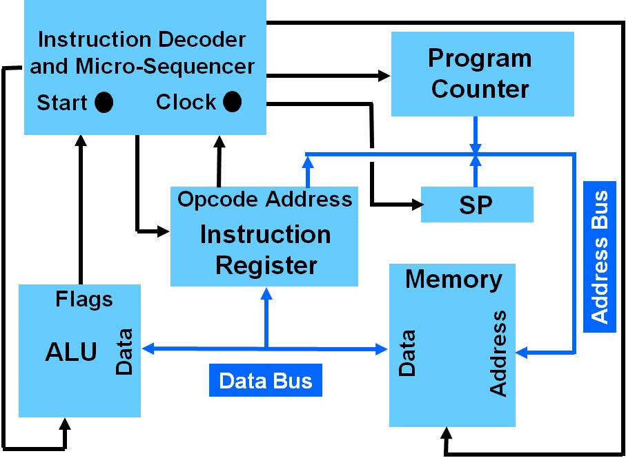
339 340
340 Adding Stack Manipulation Instructions The most common stack operations are push and pop here, the value that will be pushed and popped is the A register PSH save value in A register on stack Step 1: Decrement SP register Step 2: Store value in A register at the location pointed to by SP register POP load A with value on stack Step 1: Load A register from memory location pointed to by SP register Step 2: Increment SP register Note: The PSH and POP instructions can be used to implement expression evaluation 341
341 Adding Stack Manipulation Instructions The opcodes that will be used for PSH and POP are as follows: Opcode Mnemonic Function Performed HLT Halt stop, discontinue execution LDA addr Load A with contents of location addr ADD addr Add contents of addr to contents of A SUB addr Subtract contents of addr from contents of A AND addr AND contents of addr with contents of A STA addr Store contents of A at location addr PSH Save (A) on stack POP Restore (A) from stack 342
342 Adding Stack Manipulation Instructions At first glance, it would appear that two execute cycles are required to implement both the PSH and POP instructions As astute computer engineers, however, we always need to be on the lookout for operations that can be overlapped (subject, of course, to the rules we learned earlier): Only one device is allowed to drive a bus during any machine cycle (i.e., bus fighting must be avoided) Data cannot pass through more than one (edgetriggered) flip-flop or latch per cycle 343
343
344
345 Adding Stack Manipulation Instructions Implementation of PSH requires two execute cycles: first execute cycle: decrement SP register* (SPD) second execute cycle: output new value of SP on address bus (SPA), enable a memory write operation (MSL and MWE), and tell the ALU to output value in the A register on the data bus (AOE) *Note: The new value of SP must be available (and stable) before it can be used to address memory 346
346 347
347 348
348 Adding Stack Manipulation Instructions Implementation of POP requires only one execute cycle: first execute cycle: output value of SP on address bus (SPA), enable a memory read operation (MSL and MOE), tell the ALU to load the A register with the value on the data bus (ALE and ALX), and tell the SP register to increment* (SPI) *Note: The SP register will be incremented after the A register is loaded with the contents of the location pointed to by the SP register, i.e., the SP increment is overlapped with the fetch of the next instruction 349
349 Adding Stack Manipulation Instructions Modified system control table: Decoded State Instruction Mnemonic MSL MOE MWE PCC POA IRL S0 H H H H H Note: Recall that the RST signal is used to synchronously reset the state counter on the final execute cycle of each instruction 350 IRA AOE S1 HLT L L L L S1 LDA addr H H H H H H S1 ADD addr H H H H H S1 SUB addr H H H H H H S1 AND addr H H H H H H H S1 STA addr H H H H H S1 PSH H S1 POP H H H H H H H S2 PSH H H H H H ALE ALX ALY SPI SPD SPA RST
350 // System control equations assign MSL = RUN & (S[0] S[1] & (LDA STA ADD SUB AND POP) S[2] & PSH); assign MOE = S[0] S[1] & (LDA ADD SUB AND); assign MWE = S[1] & STA S[2] & PSH; assign ARS = START; assign PCC = RUN & S[0]; assign POA = S[0]; assign IRL = RUN & S[0]; assign IRA = S[1] & (LDA STA ADD SUB AND); assign AOE = S[1] & STA; assign ALE = RUN & S[1] & (LDA ADD SUB AND); assign ALX = S[1] & (LDA AND POP); assign ALY = S[1] & (SUB AND); assign SPI = S[1] & POP; assign SPD = S[1] & PSH; assign SPA = S[1] & POP S[2] & PSH; assign RST = S[1] & (LDA STA ADD SUB AND POP) S[2] & PSH; 351
351 Clicker Quiz 352
352 Q1. If a program contains more POP instructions than PSH instructions, the following is likely to occur: A. stack overflow (stack collides with end of program space) B. stack underflow (stack collides with beginning of program space) C. program counter overflow (program counter wraps to beginning of program space) D. program counter underflow (program counter wraps to end of program space) E. none of the above 353
353 Q2. If a program contains more PSH instructions than POP instructions, the following is likely to occur: A. stack overflow (stack collides with end of program space) B. stack underflow (stack collides with beginning of program space) C. program counter overflow (program counter wraps to beginning of program space) D. program counter underflow (program counter wraps to end of program space) E. none of the above 354
354 Adding Subroutine Linkage Instructions Why use a stack as a subroutine linkage mechanism? There are several important capabilities that a stack affords: arbitrary nesting of subroutine calls passing parameters to subroutines recursion (the ability of a subroutine to call itself) made possible by passing parameters via the stack reentrancy (the ability of a code module to be shared among quasi-simultaneously executing tasks) made possible by storing temporary local variables on the stack 355
355 Adding Subroutine Linkage Instructions The opcodes that will be used for JSR ( jump to subroutine ) and RTS ( return from subroutine ) are as follows: Opcode Mnemonic Function Performed HLT Halt stop, discontinue execution LDA addr Load A with contents of location addr ADD addr Add contents of addr to contents of A SUB addr Subtract contents of addr from contents of A AND addr AND contents of addr with contents of A STA addr Store contents of A at location addr JSR addr Jump to subroutine at location addr RTS Return from subroutine 356
356 Subroutine Linkage in Action MAIN start of main program JSR SUBA (next instruction) HLT end of main program SUBA start of subroutine A JSR SUBB (next instruction) RTS end of subroutine A SUBB start of subroutine B RTS end of subroutine B 357
357 Adding Subroutine Linkage Instructions Subroutine CALL and RETURN JSR addr jump to subroutine at memory location addr Step 1: Decrement SP register Step 2: Store return address* at location pointed to by SP register Step 3: Load PC with value in IR address field RTS return from subroutine Step 1: Load PC from memory location pointed to by SP register Step 2: Increment SP register *current value in PC, which was incremented during the fetch cycle (points to next instruction) 358
358 Adding Subroutine Linkage Instructions The astute student will realize at this point that the program counter needs to be modified a way to save its value on the stack, and subsequently restore it, must be provided Two new PC control signals need to be implemented: POD: output value of PC on data bus PLD: load PC with value on data bus 359
359 360
360 /* Program Counter with Data Bus interface */ module pc(clk, PCC, PLA, POA, RST, ADRBUS_z, DB_z, PLD, POD, PC); input wire CLK; input wire PCC; input wire PLA; input wire POA; input wire RST; input wire PLD; input wire POD; inout wire [4:0] ADRBUS_z; inout wire [7:0] DB_z; output reg [4:0] PC; // PC count enable // PC load from address bus enable // PC output on address bus tri-state enable // Asynchronous reset (connected to START) // PC load from data bus enable // PC output on data bus tri-state enable // address bus (5-bits wide) // data bus (8-bits wide) reg [4:0] next_pc; (posedge CLK, posedge RST) begin if (RST == 1'b1) PC <= 5'b00000; else PC <= next_pc; end 361
361 (PLA, PLD, PCC, AB_z, DB_z, PC) begin // synchronous control signals PLA, PLD, and PCC are mutually exclusive if (PLA == 1 b1) // load PC from address bus next_pc = ADRBUS_z; else if (PLD == 1 b1) // load PC from data bus next_pc = DB_z; else if (PCC == 1 b1) // increment PC next_pc = PC + 1; else // retain state next_pc = PC; end assign ADRBUS_z = POA? PC[4:0] : 5'bZZZZZ; assign DB_z = POD? {3'b000, PC[4:0]} : 8'bZZZZZZZZ; // pad upper 3 bits of DB w/ 0 endmodule 362
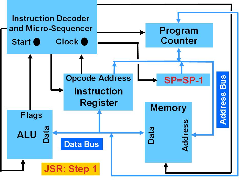
362 363
Note that none of the above MAY be a VALID ANSWER.
 ECE 270 Learning Outcome 4-1 - Practice Exam / Solution OUTCOME #4: An ability to design and implement computer logic circuits. Multiple Choice select the single most appropriate response for each question.
Chapter 3: part 3 Binary Subtraction
 Chapter 3: part 3 Binary Subtraction Iterative combinational circuits Binary adders Half and full adders Ripple carry and carry lookahead adders Binary subtraction Binary adder-subtractors Signed binary
CO Computer Architecture and Programming Languages CAPL. Lecture 9
 CO20-320241 Computer Architecture and Programming Languages CAPL Lecture 9 Dr. Kinga Lipskoch Fall 2017 A Four-bit Number Circle CAPL Fall 2017 2 / 38 Functional Parts of an ALU CAPL Fall 2017 3 / 38 Addition
DIGITAL ARITHMETIC: OPERATIONS AND CIRCUITS
 C H A P T E R 6 DIGITAL ARITHMETIC: OPERATIONS AND CIRCUITS OUTLINE 6- Binary Addition 6-2 Representing Signed Numbers 6-3 Addition in the 2 s- Complement System 6-4 Subtraction in the 2 s- Complement
Chapter 3 Part 2 Combinational Logic Design
 University of Wisconsin - Madison ECE/Comp Sci 352 Digital Systems Fundamentals Kewal K. Saluja and Yu Hen Hu Spring 2002 Chapter 3 Part 2 Combinational Logic Design Originals by: Charles R. Kime and Tom
Chapter 4 Arithmetic Functions
 Logic and Computer Design Fundamentals Chapter 4 Arithmetic Functions Charles Kime & Thomas Kaminski 2008 Pearson Education, Inc. (Hyperlinks are active in View Show mode) Overview Iterative combinational
Binary Addition. Add the binary numbers and and show the equivalent decimal addition.
 Binary Addition The rules for binary addition are 0 + 0 = 0 Sum = 0, carry = 0 0 + 1 = 0 Sum = 1, carry = 0 1 + 0 = 0 Sum = 1, carry = 0 1 + 1 = 10 Sum = 0, carry = 1 When an input carry = 1 due to a previous
Experiment 7 Arithmetic Circuits Design and Implementation
 Experiment 7 Arithmetic Circuits Design and Implementation Introduction: Addition is just what you would expect in computers. Digits are added bit by bit from right to left, with carries passed to the
CPE300: Digital System Architecture and Design
 CPE300: Digital System Architecture and Design Fall 2011 MW 17:30-18:45 CBC C316 Arithmetic Unit 10122011 http://www.egr.unlv.edu/~b1morris/cpe300/ 2 Outline Recap Fixed Point Arithmetic Addition/Subtraction
VTU NOTES QUESTION PAPERS NEWS RESULTS FORUMS Arithmetic (a) The four possible cases Carry (b) Truth table x y
 The four possible cases Carry (b) Truth table x y") Arithmetic A basic operation in all digital computers is the addition and subtraction of two numbers They are implemented, along with the basic logic functions such as AND,OR, NOT,EX- OR in the ALU subsystem
Arithmetic A basic operation in all digital computers is the addition and subtraction of two numbers They are implemented, along with the basic logic functions such as AND,OR, NOT,EX- OR in the ALU subsystem
Digital Arithmetic. Digital Arithmetic: Operations and Circuits Dr. Farahmand
 Digital Arithmetic Digital Arithmetic: Operations and Circuits Dr. Farahmand Binary Arithmetic Digital circuits are frequently used for arithmetic operations Fundamental arithmetic operations on binary
Principles of Computer Architecture. Chapter 3: Arithmetic
 3-1 Chapter 3 - Arithmetic Principles of Computer Architecture Miles Murdocca and Vincent Heuring Chapter 3: Arithmetic 3-2 Chapter 3 - Arithmetic 3.1 Overview Chapter Contents 3.2 Fixed Point Addition
COMPUTER ARITHMETIC (Part 1)
") Eastern Mediterranean University School of Computing and Technology ITEC255 Computer Organization & Architecture COMPUTER ARITHMETIC (Part 1) Introduction The two principal concerns for computer arithmetic
Eastern Mediterranean University School of Computing and Technology ITEC255 Computer Organization & Architecture COMPUTER ARITHMETIC (Part 1) Introduction The two principal concerns for computer arithmetic
Digital Circuit Design and Language. Datapath Design. Chang, Ik Joon Kyunghee University
 Digital Circuit Design and Language Datapath Design Chang, Ik Joon Kyunghee University Typical Synchronous Design + Control Section : Finite State Machine + Data Section: Adder, Multiplier, Shift Register
Chapter 4. Combinational Logic
 Chapter 4. Combinational Logic Tong In Oh 1 4.1 Introduction Combinational logic: Logic gates Output determined from only the present combination of inputs Specified by a set of Boolean functions Sequential
ECE331: Hardware Organization and Design
 ECE331: Hardware Organization and Design Lecture 9: Binary Addition & Multiplication Adapted from Computer Organization and Design, Patterson & Hennessy, UCB Pop Quiz! Using 4 bits signed integer notation:
UNIVERSITY OF MASSACHUSETTS Dept. of Electrical & Computer Engineering. Digital Computer Arithmetic ECE 666
 UNIVERSITY OF MASSACHUSETTS Dept. of Electrical & Computer Engineering Digital Computer Arithmetic ECE 666 Part 6c High-Speed Multiplication - III Israel Koren Fall 2010 ECE666/Koren Part.6c.1 Array Multipliers
EE878 Special Topics in VLSI. Computer Arithmetic for Digital Signal Processing
 EE878 Special Topics in VLSI Computer Arithmetic for Digital Signal Processing Part 6c High-Speed Multiplication - III Spring 2017 Koren Part.6c.1 Array Multipliers The two basic operations - generation
Lecture Topics. Announcements. Today: Integer Arithmetic (P&H ) Next: continued. Consulting hours. Introduction to Sim. Milestone #1 (due 1/26)
 Next: continued. Consulting hours. Introduction to Sim. Milestone #1 (due 1/26)") Lecture Topics Today: Integer Arithmetic (P&H 3.1-3.4) Next: continued 1 Announcements Consulting hours Introduction to Sim Milestone #1 (due 1/26) 2 1 Overview: Integer Operations Internal representation
Lecture Topics Today: Integer Arithmetic (P&H 3.1-3.4) Next: continued 1 Announcements Consulting hours Introduction to Sim Milestone #1 (due 1/26) 2 1 Overview: Integer Operations Internal representation
EE 109 Unit 6 Binary Arithmetic
 EE 109 Unit 6 Binary Arithmetic 1 2 Semester Transition Point At this point we are going to start to transition in our class to look more at the hardware organization and the low-level software that is
ECE 30 Introduction to Computer Engineering
 ECE 30 Introduction to Computer Engineering Study Problems, Set #6 Spring 2015 1. With x = 1111 1111 1111 1111 1011 0011 0101 0011 2 and y = 0000 0000 0000 0000 0000 0010 1101 0111 2 representing two s
ECE 341 Midterm Exam
 ECE 341 Midterm Exam Time allowed: 75 minutes Total Points: 75 Points Scored: Name: Problem No. 1 (8 points) For each of the following statements, indicate whether the statement is TRUE or FALSE: (a) A
Module 2: Computer Arithmetic
 Module 2: Computer Arithmetic 1 B O O K : C O M P U T E R O R G A N I Z A T I O N A N D D E S I G N, 3 E D, D A V I D L. P A T T E R S O N A N D J O H N L. H A N N E S S Y, M O R G A N K A U F M A N N
EE 8351 Digital Logic Circuits Ms.J.Jayaudhaya, ASP/EEE
 EE 8351 Digital Logic Circuits Ms.J.Jayaudhaya, ASP/EEE 1 Logic circuits for digital systems may be combinational or sequential. A combinational circuit consists of input variables, logic gates, and output
COMBINATIONAL LOGIC CIRCUITS
 COMBINATIONAL LOGIC CIRCUITS 4.1 INTRODUCTION The digital system consists of two types of circuits, namely: (i) Combinational circuits and (ii) Sequential circuits A combinational circuit consists of logic
DLD VIDYA SAGAR P. potharajuvidyasagar.wordpress.com. Vignana Bharathi Institute of Technology UNIT 3 DLD P VIDYA SAGAR
 DLD UNIT III Combinational Circuits (CC), Analysis procedure, Design Procedure, Combinational circuit for different code converters and other problems, Binary Adder- Subtractor, Decimal Adder, Binary Multiplier,
Chapter 5 Design and Implementation of a Unified BCD/Binary Adder/Subtractor
 Chapter 5 Design and Implementation of a Unified BCD/Binary Adder/Subtractor Contents Chapter 5... 74 5.1 Introduction... 74 5.2 Review of Existing Techniques for BCD Addition/Subtraction... 76 5.2.1 One-Digit
 CS6303 COMPUTER ARCHITECTURE LESSION NOTES UNIT II ARITHMETIC OPERATIONS ALU In computing an arithmetic logic unit (ALU) is a digital circuit that performs arithmetic and logical operations. The ALU is
Microcomputers. Outline. Number Systems and Digital Logic Review
 Microcomputers Number Systems and Digital Logic Review Lecture 1-1 Outline Number systems and formats Common number systems Base Conversion Integer representation Signed integer representation Binary coded
Korea University of Technology and Education
 MEC52 디지털공학 Binary Systems Jee-Hwan Ryu School of Mechanical Engineering Binary Numbers a 5 a 4 a 3 a 2 a a.a - a -2 a -3 base or radix = a n r n a n- r n-...a 2 r 2 a ra a - r - a -2 r -2...a -m r -m
Combinational Logic Circuits
 Combinational Logic Circuits By Dr. M. Hebaishy Digital Logic Design Ch- Rem.!) Types of Logic Circuits Combinational Logic Memoryless Outputs determined by current values of inputs Sequential Logic Has
Chapter 3 Arithmetic for Computers
 Chapter 3 Arithmetic for Computers 1 Arithmetic Where we've been: Abstractions: Instruction Set Architecture Assembly Language and Machine Language What's up ahead: Implementing the Architecture operation
D I G I T A L C I R C U I T S E E
 D I G I T A L C I R C U I T S E E Digital Circuits Basic Scope and Introduction This book covers theory solved examples and previous year gate question for following topics: Number system, Boolean algebra,
LOGIC CIRCUITS. Kirti P_Didital Design 1
 LOGIC CIRCUITS Kirti P_Didital Design 1 Introduction The digital system consists of two types of circuits, namely (i) Combinational circuits and (ii) Sequential circuit A combinational circuit consists
Digital Systems and Binary Numbers
 Digital Systems and Binary Numbers Prof. Wangrok Oh Dept. of Information Communications Eng. Chungnam National University Prof. Wangrok Oh(CNU) 1 / 51 Overview 1 Course Summary 2 Binary Numbers 3 Number-Base
Combinational Logic II
 Combinational Logic II Ranga Rodrigo July 26, 2009 1 Binary Adder-Subtractor Digital computers perform variety of information processing tasks. Among the functions encountered are the various arithmetic
COMPUTER ARCHITECTURE AND ORGANIZATION Register Transfer and Micro-operations 1. Introduction A digital system is an interconnection of digital
 Register Transfer and Micro-operations 1. Introduction A digital system is an interconnection of digital hardware modules that accomplish a specific information-processing task. Digital systems vary in
Number System. Introduction. Decimal Numbers
 Number System Introduction Number systems provide the basis for all operations in information processing systems. In a number system the information is divided into a group of symbols; for example, 26
ELECTRICAL AND COMPUTER ENGINEERING DEPARTMENT, OAKLAND UNIVERSITY ECE-2700: Digital Logic Design Winter Notes - Unit 4. hundreds.
 UNSIGNED INTEGER NUMBERS Notes - Unit 4 DECIMAL NUMBER SYSTEM A decimal digit can take values from to 9: Digit-by-digit representation of a positive integer number (powers of ): DIGIT 3 4 5 6 7 8 9 Number:
ECE/Comp Sci 352 Digital Systems Fundamentals. Charles R. Kime Section 2 Fall Logic and Computer Design Fundamentals
 University of Wisconsin - Madison ECE/Comp Sci 352 Digital Systems Fundamentals Charles R. Kime Section 2 Fall 2001 Chapter 3 Combinational Logic Design Part 4 Charles Kime & Thomas Kaminski Complements
Logic Circuits I ECE 1411 Thursday 4:45pm-7:20pm. Nathan Pihlstrom.
 Logic Circuits I ECE 1411 Thursday 4:45pm-7:20pm Nathan Pihlstrom www.uccs.edu/~npihlstr My Background B.S.E.E. from Colorado State University M.S.E.E. from Colorado State University M.B.A. from UCCS Ford
Chapter 10 - Computer Arithmetic
 Chapter 10 - Computer Arithmetic Luis Tarrataca luis.tarrataca@gmail.com CEFET-RJ L. Tarrataca Chapter 10 - Computer Arithmetic 1 / 126 1 Motivation 2 Arithmetic and Logic Unit 3 Integer representation
Binary Arithmetic. Daniel Sanchez Computer Science & Artificial Intelligence Lab M.I.T.
 Binary Arithmetic Daniel Sanchez Computer Science & Artificial Intelligence Lab M.I.T. MIT 6.004 Fall 2018 Reminder: Encoding Positive Integers Bit i in a binary representation (in right-to-left order)
Lecture (02) Operations on numbering systems
 Operations on numbering systems") Lecture (02) Operations on numbering systems By: Dr. Ahmed ElShafee ١ Dr. Ahmed ElShafee, ACU : Spring 2018, CSE202 Logic Design I Complements of a number Complements are used in digital computers to simplify
Lecture (02) Operations on numbering systems By: Dr. Ahmed ElShafee ١ Dr. Ahmed ElShafee, ACU : Spring 2018, CSE202 Logic Design I Complements of a number Complements are used in digital computers to simplify
Parallel logic circuits
 Computer Mathematics Week 9 Parallel logic circuits College of Information cience and Engineering Ritsumeikan University last week the mathematics of logic circuits the foundation of all digital design
(+A) + ( B) + (A B) (B A) + (A B) ( A) + (+ B) (A B) + (B A) + (A B) (+ A) (+ B) + (A - B) (B A) + (A B) ( A) ( B) (A B) + (B A) + (A B)
 + ( B) + (A B) (B A) + (A B) ( A) + (+ B) (A B) + (B A) + (A B) (+ A) (+ B) + (A - B) (B A) + (A B) ( A) ( B) (A B) + (B A) + (A B)") COMPUTER ARITHMETIC 1. Addition and Subtraction of Unsigned Numbers The direct method of subtraction taught in elementary schools uses the borrowconcept. In this method we borrow a 1 from a higher significant
COMPUTER ARITHMETIC 1. Addition and Subtraction of Unsigned Numbers The direct method of subtraction taught in elementary schools uses the borrowconcept. In this method we borrow a 1 from a higher significant
Binary Adders: Half Adders and Full Adders
 Binary Adders: Half Adders and Full Adders In this set of slides, we present the two basic types of adders: 1. Half adders, and 2. Full adders. Each type of adder functions to add two binary bits. In order
Combinational Logic. Prof. Wangrok Oh. Dept. of Information Communications Eng. Chungnam National University. Prof. Wangrok Oh(CNU) 1 / 93
 1 / 93") Combinational Logic Prof. Wangrok Oh Dept. of Information Communications Eng. Chungnam National University Prof. Wangrok Oh(CNU) / 93 Overview Introduction 2 Combinational Circuits 3 Analysis Procedure
Combinational Logic Prof. Wangrok Oh Dept. of Information Communications Eng. Chungnam National University Prof. Wangrok Oh(CNU) / 93 Overview Introduction 2 Combinational Circuits 3 Analysis Procedure
ECE 341 Midterm Exam
 ECE 341 Midterm Exam Time allowed: 90 minutes Total Points: 75 Points Scored: Name: Problem No. 1 (10 points) For each of the following statements, indicate whether the statement is TRUE or FALSE: (a)
Computer Architecture and Organization
 3-1 Chapter 3 - Arithmetic Computer Architecture and Organization Miles Murdocca and Vincent Heuring Chapter 3 Arithmetic 3-2 Chapter 3 - Arithmetic Chapter Contents 3.1 Fixed Point Addition and Subtraction
Array Multipliers. Figure 6.9 The partial products generated in a 5 x 5 multiplication. Sec. 6.5
 Sec. 6.5 Array Multipliers I'r) 1'8 P7 p6 PS f'4 1'3 1'2 1' 1 "0 Figure 6.9 The partial products generated in a 5 x 5 multiplication. called itemrive arrc.ly multipliers or simply cirruy m~illil>liers.
NH 67, Karur Trichy Highways, Puliyur C.F, Karur District UNIT-II COMBINATIONAL CIRCUITS
 NH 67, Karur Trichy Highways, Puliyur C.F, 639 114 Karur District DEPARTMENT OF ELETRONICS AND COMMUNICATION ENGINEERING COURSE NOTES SUBJECT: DIGITAL ELECTRONICS CLASS: II YEAR ECE SUBJECT CODE: EC2203
Combinational Circuits
 Combinational Circuits Combinational circuit consists of an interconnection of logic gates They react to their inputs and produce their outputs by transforming binary information n input binary variables
UNIT-II. Part-2: CENTRAL PROCESSING UNIT
 Page1 UNIT-II Part-2: CENTRAL PROCESSING UNIT Stack Organization Instruction Formats Addressing Modes Data Transfer And Manipulation Program Control Reduced Instruction Set Computer (RISC) Introduction:
Department of Electrical and Computer Engineering University of Wisconsin - Madison. ECE/CS 352 Digital System Fundamentals.
 Department of Electrical and Computer Engineering University of Wisconsin - Madison ECE/C 352 Digital ystem Fundamentals Quiz #2 Thursday, March 7, 22, 7:15--8:3PM 1. (15 points) (a) (5 points) NAND, NOR
ELECTRICAL AND COMPUTER ENGINEERING DEPARTMENT, OAKLAND UNIVERSITY ECE-278: Digital Logic Design Fall Notes - Unit 4. hundreds.
 ECE-78: Digital Logic Design Fall 6 UNSIGNED INTEGER NUMBERS Notes - Unit 4 DECIMAL NUMBER SYSTEM A decimal digit can take values from to 9: Digit-by-digit representation of a positive integer number (powers
CPE 323 REVIEW DATA TYPES AND NUMBER REPRESENTATIONS IN MODERN COMPUTERS
 CPE 323 REVIEW DATA TYPES AND NUMBER REPRESENTATIONS IN MODERN COMPUTERS Aleksandar Milenković The LaCASA Laboratory, ECE Department, The University of Alabama in Huntsville Email: milenka@uah.edu Web:
Area Efficient, Low Power Array Multiplier for Signed and Unsigned Number. Chapter 3
 Area Efficient, Low Power Array Multiplier for Signed and Unsigned Number Chapter 3 Area Efficient, Low Power Array Multiplier for Signed and Unsigned Number Chapter 3 3.1 Introduction The various sections
CHAPTER 6 ARITHMETIC, LOGIC INSTRUCTIONS, AND PROGRAMS
 CHAPTER 6 ARITHMETIC, LOGIC INSTRUCTIONS, AND PROGRAMS Addition of Unsigned Numbers The instruction ADD is used to add two operands Destination operand is always in register A Source operand can be a register,
ECEN 468 Advanced Logic Design
 ECEN 468 Advanced Logic Design Lecture 26: Verilog Operators ECEN 468 Lecture 26 Operators Operator Number of Operands Result Arithmetic 2 Binary word Bitwise 2 Binary word Reduction 1 Bit Logical 2 Boolean
Arithmetic Circuits. Nurul Hazlina Adder 2. Multiplier 3. Arithmetic Logic Unit (ALU) 4. HDL for Arithmetic Circuit
 4. HDL for Arithmetic Circuit") Nurul Hazlina 1 1. Adder 2. Multiplier 3. Arithmetic Logic Unit (ALU) 4. HDL for Arithmetic Circuit Nurul Hazlina 2 Introduction 1. Digital circuits are frequently used for arithmetic operations 2. Fundamental
Nurul Hazlina 1 1. Adder 2. Multiplier 3. Arithmetic Logic Unit (ALU) 4. HDL for Arithmetic Circuit Nurul Hazlina 2 Introduction 1. Digital circuits are frequently used for arithmetic operations 2. Fundamental
Final Exam Solution Sunday, December 15, 10:05-12:05 PM
 Last (family) name: First (given) name: Student I.D. #: Circle section: Kim Hu Department of Electrical and Computer Engineering University of Wisconsin - Madison ECE/CS 352 Digital System Fundamentals
10.1. Unit 10. Signed Representation Systems Binary Arithmetic
 0. Unit 0 Signed Representation Systems Binary Arithmetic 0.2 BINARY REPRESENTATION SYSTEMS REVIEW 0.3 Interpreting Binary Strings Given a string of s and 0 s, you need to know the representation system
Chapter 1 Review of Number Systems
 1.1 Introduction Chapter 1 Review of Number Systems Before the inception of digital computers, the only number system that was in common use is the decimal number system which has a total of 10 digits
NH 67, Karur Trichy Highways, Puliyur C.F, Karur District DEPARTMENT OF INFORMATION TECHNOLOGY CS 2202 DIGITAL PRINCIPLES AND SYSTEM DESIGN
 NH 67, Karur Trichy Highways, Puliyur C.F, 639 114 Karur District DEPARTMENT OF INFORMATION TECHNOLOGY CS 2202 DIGITAL PRINCIPLES AND SYSTEM DESIGN UNIT 2 COMBINATIONAL LOGIC Combinational circuits Analysis
UNIT - V MEMORY P.VIDYA SAGAR ( ASSOCIATE PROFESSOR) Department of Electronics and Communication Engineering, VBIT
 Department of Electronics and Communication Engineering, VBIT") UNIT - V MEMORY P.VIDYA SAGAR ( ASSOCIATE PROFESSOR) contents Memory: Introduction, Random-Access memory, Memory decoding, ROM, Programmable Logic Array, Programmable Array Logic, Sequential programmable
UNIT - V MEMORY P.VIDYA SAGAR ( ASSOCIATE PROFESSOR) contents Memory: Introduction, Random-Access memory, Memory decoding, ROM, Programmable Logic Array, Programmable Array Logic, Sequential programmable
Logic, Words, and Integers
 Computer Science 52 Logic, Words, and Integers 1 Words and Data The basic unit of information in a computer is the bit; it is simply a quantity that takes one of two values, 0 or 1. A sequence of k bits
IA Digital Electronics - Supervision I
 IA Digital Electronics - Supervision I Nandor Licker Due noon two days before the supervision 1 Overview The goal of this exercise is to design an 8-digit calculator capable of adding
CPE 323 REVIEW DATA TYPES AND NUMBER REPRESENTATIONS IN MODERN COMPUTERS
 CPE 323 REVIEW DATA TYPES AND NUMBER REPRESENTATIONS IN MODERN COMPUTERS Aleksandar Milenković The LaCASA Laboratory, ECE Department, The University of Alabama in Huntsville Email: milenka@uah.edu Web:
EC2303-COMPUTER ARCHITECTURE AND ORGANIZATION
 EC2303-COMPUTER ARCHITECTURE AND ORGANIZATION QUESTION BANK UNIT-II 1. What are the disadvantages in using a ripple carry adder? (NOV/DEC 2006) The main disadvantage using ripple carry adder is time delay.
UNIT - I: COMPUTER ARITHMETIC, REGISTER TRANSFER LANGUAGE & MICROOPERATIONS
 UNIT - I: COMPUTER ARITHMETIC, REGISTER TRANSFER LANGUAGE & MICROOPERATIONS (09 periods) Computer Arithmetic: Data Representation, Fixed Point Representation, Floating Point Representation, Addition and
CHAPTER V NUMBER SYSTEMS AND ARITHMETIC
 CHAPTER V-1 CHAPTER V CHAPTER V NUMBER SYSTEMS AND ARITHMETIC CHAPTER V-2 NUMBER SYSTEMS RADIX-R REPRESENTATION Decimal number expansion 73625 10 = ( 7 10 4 ) + ( 3 10 3 ) + ( 6 10 2 ) + ( 2 10 1 ) +(
Lecture (03) Binary Codes Registers and Logic Gates
 Binary Codes Registers and Logic Gates") Lecture (03) Binary Codes Registers and Logic Gates By: Dr. Ahmed ElShafee Binary Codes Digital systems use signals that have two distinct values and circuit elements that have two stable states. binary
Lecture (03) Binary Codes Registers and Logic Gates By: Dr. Ahmed ElShafee Binary Codes Digital systems use signals that have two distinct values and circuit elements that have two stable states. binary
Addition and multiplication
 Addition and multiplication Arithmetic is the most basic thing you can do with a computer, but it s not as easy as you might expect! These next few lectures focus on addition, subtraction, multiplication
Chapter Three. Digital Components
 Chapter Three 3.1. Combinational Circuit A combinational circuit is a connected arrangement of logic gates with a set of inputs and outputs. The binary values of the outputs are a function of the binary
Digital Computer Arithmetic
 Digital Computer Arithmetic Part 6 High-Speed Multiplication Soo-Ik Chae Spring 2010 Koren Chap.6.1 Speeding Up Multiplication Multiplication involves 2 basic operations generation of partial products
CHAPTER TWO. Data Representation ( M.MORRIS MANO COMPUTER SYSTEM ARCHITECTURE THIRD EDITION ) IN THIS CHAPTER
 IN THIS CHAPTER") 1 CHAPTER TWO Data Representation ( M.MORRIS MANO COMPUTER SYSTEM ARCHITECTURE THIRD EDITION ) IN THIS CHAPTER 2-1 Data Types 2-2 Complements 2-3 Fixed-Point Representation 2-4 Floating-Point Representation
1 CHAPTER TWO Data Representation ( M.MORRIS MANO COMPUTER SYSTEM ARCHITECTURE THIRD EDITION ) IN THIS CHAPTER 2-1 Data Types 2-2 Complements 2-3 Fixed-Point Representation 2-4 Floating-Point Representation
Semester Transition Point. EE 109 Unit 11 Binary Arithmetic. Binary Arithmetic ARITHMETIC
 1 2 Semester Transition Point EE 109 Unit 11 Binary Arithmetic At this point we are going to start to transition in our class to look more at the hardware organization and the low-level software that is
Computer Architecture and Organization: L04: Micro-operations
 Computer Architecture and Organization: L4: Micro-operations By: A. H. Abdul Hafez Abdul.hafez@hku.edu.tr, ah.abdulhafez@gmail.com, hafez@research.iiit.ac.in 1 Outlines 1. Arithmetic microoperation 2.
CPE 335 Computer Organization. MIPS Arithmetic Part I. Content from Chapter 3 and Appendix B
 CPE 335 Computer Organization MIPS Arithmetic Part I Content from Chapter 3 and Appendix B Dr. Iyad Jafar Adatped from Dr. Gheith Abandah Slides http://www.abandah.com/gheith/courses/cpe335_s08/index.html
 UNIT II - COMBINATIONAL LOGIC Part A 2 Marks. 1. Define Combinational circuit A combinational circuit consist of logic gates whose outputs at anytime are determined directly from the present combination
Arithmetic Processing
 CS/EE 5830/6830 VLSI ARCHITECTURE Chapter 1 Basic Number Representations and Arithmetic Algorithms Arithmetic Processing AP = (operands, operation, results, conditions, singularities) Operands are: Set
carry in carry 1101 carry carry
 Chapter Binary arithmetic Arithmetic is the process of applying a mathematical operator (such as negation or addition) to one or more operands (the values being operated upon). Binary arithmetic works
Number Systems and Computer Arithmetic
 Number Systems and Computer Arithmetic Counting to four billion two fingers at a time What do all those bits mean now? bits (011011011100010...01) instruction R-format I-format... integer data number text
Advanced Computer Architecture-CS501
 Advanced Computer Architecture Lecture No. 34 Reading Material Vincent P. Heuring & Harry F. Jordan Chapter 6 Computer Systems Design and Architecture 6.1, 6.2 Summary Introduction to ALSU Radix Conversion
Chapter 3: Arithmetic for Computers
 Chapter 3: Arithmetic for Computers Objectives Signed and Unsigned Numbers Addition and Subtraction Multiplication and Division Floating Point Computer Architecture CS 35101-002 2 The Binary Numbering
Chapter 3 Part 2 Combinational Logic Design
 University of Wisconsin - Madison EE/omp ci 352 Digital ystems Fundamentals Kewal K. aluja and u Hen Hu pring 2002 hapter 3 Part 2 ombinational Logic Design Originals by: harles R. Kime and Tom Kamisnski
Outline. Introduction to Structured VLSI Design. Signed and Unsigned Integers. 8 bit Signed/Unsigned Integers
 Outline Introduction to Structured VLSI Design Integer Arithmetic and Pipelining Multiplication in the digital domain HW mapping Pipelining optimization Joachim Rodrigues Signed and Unsigned Integers n-1
Computer Organization
 Register Transfer Logic Department of Computer Science Missouri University of Science & Technology hurson@mst.edu 1 Note, this unit will be covered in three lectures. In case you finish it earlier, then
A complement number system is used to represent positive and negative integers. A complement number system is based on a fixed length representation
 Complement Number Systems A complement number system is used to represent positive and negative integers A complement number system is based on a fixed length representation of numbers Pretend that integers
EECS150 - Digital Design Lecture 13 - Combinational Logic & Arithmetic Circuits Part 3
 EECS15 - Digital Design Lecture 13 - Combinational Logic & Arithmetic Circuits Part 3 October 8, 22 John Wawrzynek Fall 22 EECS15 - Lec13-cla3 Page 1 Multiplication a 3 a 2 a 1 a Multiplicand b 3 b 2 b
Lecture Topics. Announcements. Today: Integer Arithmetic (P&H ) Next: The MIPS ISA (P&H ) Consulting hours. Milestone #1 (due 1/26)
 Next: The MIPS ISA (P&H ) Consulting hours. Milestone #1 (due 1/26)") Lecture Topics Today: Integer Arithmetic (P&H 3.1-3.4) Next: The MIPS ISA (P&H 2.1-2.14) 1 Announcements Consulting hours Milestone #1 (due 1/26) Milestone #2 (due 2/2) 2 1 Review: Integer Operations Internal
Lecture Topics Today: Integer Arithmetic (P&H 3.1-3.4) Next: The MIPS ISA (P&H 2.1-2.14) 1 Announcements Consulting hours Milestone #1 (due 1/26) Milestone #2 (due 2/2) 2 1 Review: Integer Operations Internal
Chapter 10 Binary Arithmetics
 27..27 Chapter Binary Arithmetics Dr.-Ing. Stefan Werner Table of content Chapter : Switching Algebra Chapter 2: Logical Levels, Timing & Delays Chapter 3: Karnaugh-Veitch-Maps Chapter 4: Combinational
Real Digital Problem Set #6
 Real igital Problem et #6. (2 points) ketch a block diagram for a magnitude comparator bit-slice circuit. Create K-maps to define the bit-slice circuit, and use them to find optimal logic equations. ketch
BINARY SYSTEM. Binary system is used in digital systems because it is:
 CHAPTER 2 CHAPTER CONTENTS 2.1 Binary System 2.2 Binary Arithmetic Operation 2.3 Signed & Unsigned Numbers 2.4 Arithmetic Operations of Signed Numbers 2.5 Hexadecimal Number System 2.6 Octal Number System
MGU-BCA-205- Second Sem- Core VI- Fundamentals of Digital Systems- MCQ s. 2. Why the decimal number system is also called as positional number system?
 MGU-BCA-205- Second Sem- Core VI- Fundamentals of Digital Systems- MCQ s Unit-1 Number Systems 1. What does a decimal number represents? A. Quality B. Quantity C. Position D. None of the above 2. Why the
II/IV B.Tech (Regular/Supplementary) DEGREE EXAMINATION. Answer ONE question from each unit.
 DEGREE EXAMINATION. Answer ONE question from each unit.") Hall Ticket Number: 14CS IT303 November, 2017 Third Semester Time: Three Hours Answer Question No.1 compulsorily. II/IV B.Tech (Regular/Supplementary) DEGREE EXAMINATION Common for CSE & IT Digital Logic
Hall Ticket Number: 14CS IT303 November, 2017 Third Semester Time: Three Hours Answer Question No.1 compulsorily. II/IV B.Tech (Regular/Supplementary) DEGREE EXAMINATION Common for CSE & IT Digital Logic
COE 202: Digital Logic Design Number Systems Part 2. Dr. Ahmad Almulhem ahmadsm AT kfupm Phone: Office:
 COE 0: Digital Logic Design Number Systems Part Dr. Ahmad Almulhem Email: ahmadsm AT kfupm Phone: 860-7554 Office: -34 Objectives Arithmetic operations: Binary number system Other number systems Base Conversion
CO212 Lecture 10: Arithmetic & Logical Unit
 CO212 Lecture 10: Arithmetic & Logical Unit Shobhanjana Kalita, Dept. of CSE, Tezpur University Slides courtesy: Computer Architecture and Organization, 9 th Ed, W. Stallings Integer Representation For
2. (a) Compare the characteristics of a floppy disk and a hard disk. (b) Discuss in detail memory interleaving. [8+7]
![2. (a) Compare the characteristics of a floppy disk and a hard disk. (b) Discuss in detail memory interleaving. [8+7]](/thumbs/96/127320205.jpg "2. (a) Compare the characteristics of a floppy disk and a hard disk. (b) Discuss in detail memory interleaving. [8+7]") Code No: A109211202 R09 Set No. 2 1. (a) Explain the purpose of the following registers: i. IR ii. PC iii. MDR iv. MAR. (b) Explain with an example the steps in subtraction of two n-digit unsigned numbers.
Code No: A109211202 R09 Set No. 2 1. (a) Explain the purpose of the following registers: i. IR ii. PC iii. MDR iv. MAR. (b) Explain with an example the steps in subtraction of two n-digit unsigned numbers.