Open access to photonic integration technologies
|
|
|
- Kristopher Bryant
- 5 years ago
- Views:
Transcription
1 Open access to photonic integration technologies Academic and Industrial examples of photonic integrated circuits Katarzyna Ławniczuk
2 What is photonic integration technology? multiple optical components on a single chip in less than cm2 2
3 What is photonic integration technology? multiple optical components on a single chip in less than cm2 light propagation light detection light amplification and generation light modulation (phase and amplitude) 3
4 What is photonic integration technology? Photonic building blocks: waveguide amplifier detector modulator 4
5 What is photonic integration technology? Advantages: Miniaturization Cost reduction Performance enhancement Photonic building blocks: waveguide amplifier detector modulator 5


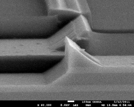
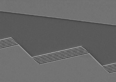
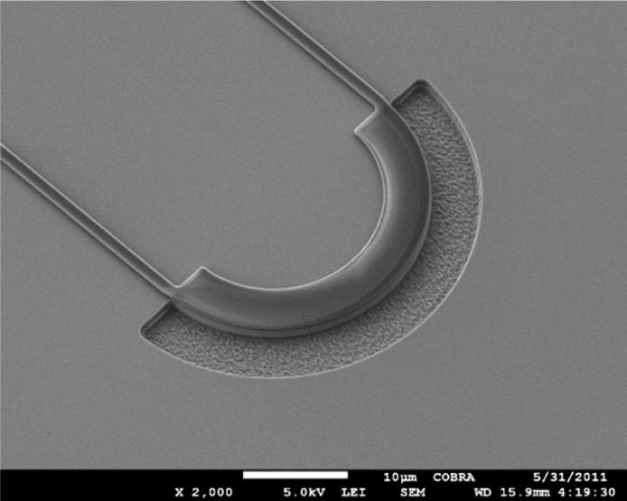
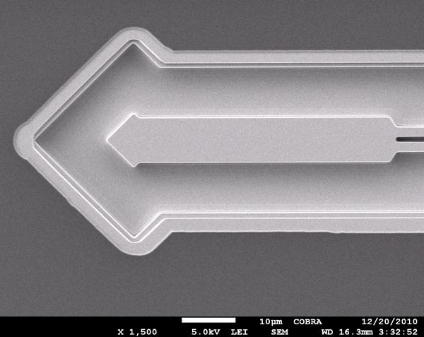
6 Basic Building blocks : optical waveguide human hair Waveguide SEM image 75 μm 6


7 Photonic Building Blocks


8 Open Access to technology: MPW runs Multi Project Wafer runs Access to a cutting edge photonic technology Sharing wafer : sharing fab costs Simple and cheap way of prototyping Fabless business model 8
9 Implementing new designs JePPIX: broker InP and TriPleX 9


10 B JePPIX: broker InP and TriPleX Value chain for photonic ICs prototyping 10

11 Where to use PIC technology? Telecom and Datacom Switching, FTTH, RoF, OTDM, DWDM Sensor readouts FBG interrogators Spectrometers Medical and diagnostic OCT, bio imaging Microwave, THZ and RF photonics Quantum communication Variety of lasers Widely tunable, multiwavelength Ring and pulse lasers And many more 11
 @1 khz Sampling Speeds up to 20 MHz 50 unique FBG sensors per single fiber (20 khz, 10fmΔλ) 10x 10x")
12 World Records in sensing! Measurement Resolution of 0.02 fmδλ (~ 0.02 nano khz Sampling Speeds up to 20 MHz 50 unique FBG sensors per single fiber (20 khz, 10fmΔλ) 10x 10x 100x 1000x smaller cheaper faster more accurate 12
 @1 khz Sampling Speeds up to 20 MHz 50 unique FBG sensors per single fiber (20 khz, 10fmΔλ) 10x")
13 World Records in sensing! Measurement Resolution of 0.02 fmδλ (~ 0.02 nano khz Sampling Speeds up to 20 MHz 50 unique FBG sensors per single fiber (20 khz, 10fmΔλ) 10x smaller 10x cheaper 100x faster 1000x more accurate 13


14 Optical beam forming network units: 4G and 5G Application: 4G and 5G steerable antennas in aviation market and RF communication market System based on integrated optics optical beam forming network (IO OBFN) Radical miniaturization and cost reduction 20x increase of bandwidth No mechanically moving parts: enhanced stability 14


15 Ultra wideband tuning range! Precision electronic tuning and Ultra wide band tuning at 72 nm Identify high order absorption lines Gas detection and spectral signature recognition: S. Latkowski, ICTON 2014 Multi species detection Explosives detection Disease prevention, Quality control 15

16 Ultra wideband tuning range! Precision electronic tuning and Ultra wide band tuning at 72 nm Identify high order absorption lines Gas detection and spectral signature recognition: S. Latkowski, ICTON 2014 Multi species detection Explosives detection Disease prevention, Quality control 16


17 Lidar and free space optical communications using optical phased arrays Electro optic control of coherent emitter array for lensless beam shaping and high speed, non mechanical beam scanning; Mature telecom nm enable coherent detection, high speed modulation; 1550 nm is eye safe and invisible to nightvision Doylend et al., Optics Express 19, 22 (2011) Hulme et al., Optics Express, 23, 5 (2015)
18 cleanroom (800 m2)
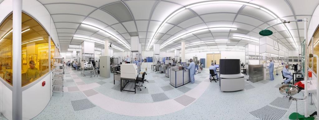
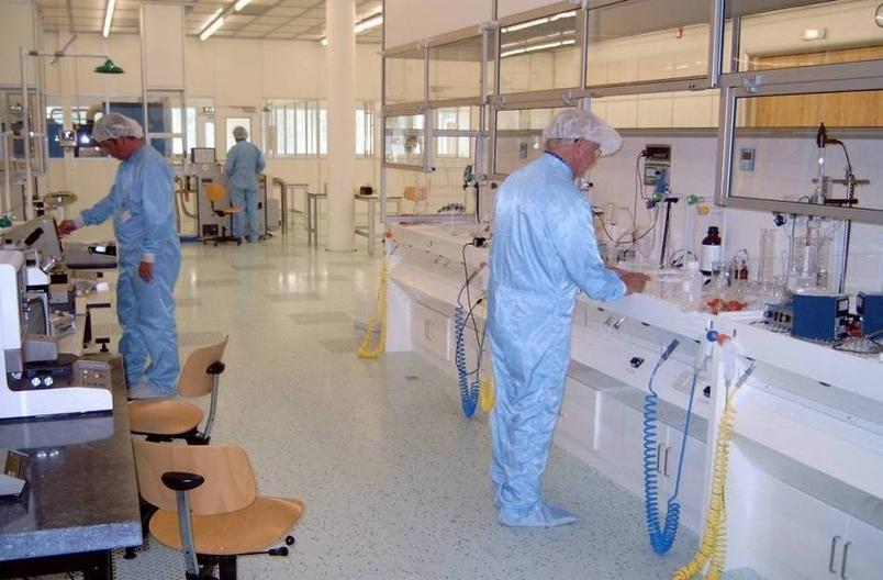
19 B NanoLab@TU/e cleanroom (800 m2)
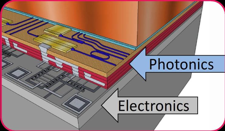
20 Further development: electronic photonic integration Ring laser in IMOS InP membrane on silicon (IMOS) 20


21 Platforms development: new, improved functionality MMI reflector Fabrication-Tolerant Polarization Converters Low reflection splitters Microbends 20 μm AWG through deep UV lithography 21


22 PICs4All: pics4all.jeppix.eu Free advice on the applicability of PIC technology; Create European network of Application Support Centers ACTPHAST: actphast.eu One stop shop solution for supporting photonics innovation in European companies Innovation Support EU funds 22
 Coupling to photonic integrated circuits 4) Compact")
 Ultrafest optical pulse amplification")
 Grating optimization using genetic")
 Magnetic claddings for Photonic Integrated circuits Open")
23 Graduate Projects 1) High speed photonic ICs 2) Integrated spectrometry 3) Coupling to photonic integrated circuits 4) Compact laser model 5) Metal nano grating couplers 6) Generation of stabilized frequency combs 7) Ultrafest optical pulse amplification and shaping 8) Corner mirror 9) Design of an active/passive integrated membrane DBR laser 10) Grating optimization using genetic algorithms 11) Plasma etching technique for aluminum based lasers 12) Magnetic claddings for Photonic Integrated circuits Open positions 23
24 PIC Measurements Engineer develop and perform measurement and analysis methods for advanced photonic ICs. Postdoc Position: InP Membrane On Silicon platform explore the essential technologies required for the platform focus on processing InP based circuits on top of a silicon or (Bi)CMOS wafer. Open positions 24

25 Thank you!
PIC design across platforms. Ronald Broeke Bright Photonics
 PIC design across platforms Ronald Broeke Bright Photonics OUTLINE Introduction PIC applications & designs MPW Materials & platforms Design modules PICs in Phoxtrot Design House for Photonics ICs Custom
Packaging and Integration Technologies for Silicon Photonics. Dr. Peter O Brien, Tyndall National Institute, Ireland.
 Packaging and Integration Technologies for Silicon Photonics Dr. Peter O Brien, Tyndall National Institute, Ireland. Opportunities for Silicon Photonics Stress Sensors Active Optical Cable 300 mm Silicon
Introduction of the Industry's Broadest Tunable Quantum Cascade Lasers. February Block Engineering 1
 Introduction of the Industry's Broadest Tunable Quantum Cascade Lasers February 2014 2014 Block Engineering 1 Widely-Tunable QCL Products LaserTune Mini-QCL Smallest widely-tunable QCL source Embedded
Pump laser requirements for next generation lasers.
 Dr. Lukas Krainer, CEO lukas.krainer@onefive.com Pump laser requirements for next generation lasers. Outline Company introduction Product portfolio Pump lasers field of use Pump lasers for high power cw
Imaging, BiCMOS ASIC and Silicon Photonics. Eric Aussedat Executive Vice President General Manager, Imaging, Bi-CMOS ASIC and Silicon Photonics Group
 Imaging, BiCMOS ASIC and Silicon Photonics Eric Aussedat Executive Vice President General Manager, Imaging, Bi-CMOS ASIC and Silicon Photonics Group IBP Leading Position Targets 2 Image Sensors Solutions
PLANAR LIGHTWAVE CIRCUITS FOR USE IN ADVANCED OPTICAL INSTRUMENTATION
 PLANAR LIGHTWAVE CIRCUITS FOR USE IN ADVANCED OPTICAL INSTRUMENTATION AN ENABLENCE ARTICLE WRITTEN BY DR. MATT PEARSON, VP TECHNOLOGY & ASHOK BALAKRISHNAN, DIRECTOR OF PRODUCT DEVELOPMENT PUBLISHED IN
Kotura Analysis: WDM PICs improve cost over LR4
 Kotura Analysis: WDM PICs improve cost over LR4 IEEE P802.3bm - 40 Gb/s & 100 Gb/s Fiber Optic Task Force Sept 2012 Contributors: Mehdi Asghari, Kotura Samir Desai, Kotura Arlon Martin, Kotura Recall the
2000 Technology Roadmap Optoelectronics. John Stafford, Motorola January 17, 2001
 2000 Technology Roadmap Optoelectronics John Stafford, Motorola January 17, 2001 Optoelectronic Roadmap Agenda Optoelectronics Market Overview Optical Communications Roadmap Optical Communications Technology
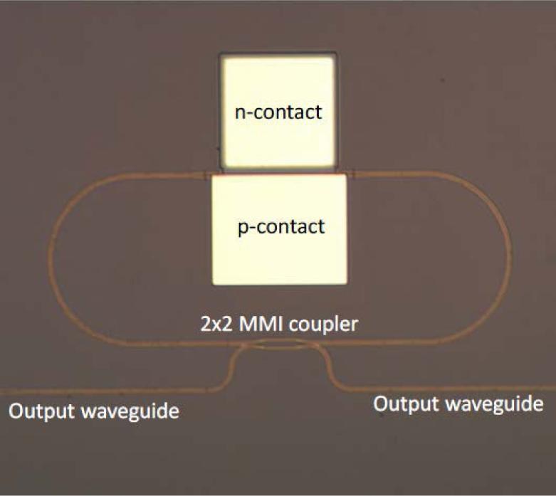
MMI reflectors with free selection of reflection to transmission ratio Kleijn, E.; Vries, de, T.; Ambrosius, H.P.M.M.; Smit, M.K.; Leijtens, X.J.M.
 MMI reflectors with free selection of reflection to transmission ratio Kleijn, E.; Vries, de, T.; Ambrosius, H.P.M.M.; Smit, M.K.; Leijtens, X.J.M. Published in: Proceedings of the 15th Annual Symposium
Organics in Photonics: Opportunities & Challenges. Louay Eldada DuPont Photonics Technologies
 Organics in Photonics: Opportunities & Challenges Louay Eldada DuPont Photonics Technologies Market Drivers for Organic Photonics Telecom Application Product Examples Requirements What Organics Offer Dynamic
MARKET PERSPECTIVE: SEMICONDUCTOR TREND OF 2.5D/3D IC WITH OPTICAL INTERFACES PHILIPPE ABSIL, IMEC
 MARKET PERSPECTIVE: SEMICONDUCTOR TREND OF 2.5D/3D IC WITH OPTICAL INTERFACES PHILIPPE ABSIL, IMEC OUTLINE Market Trends & Technology Needs Silicon Photonics Technology Remaining Key Challenges Conclusion
Study of 1x4 Optical Power Splitters with Optical Network
 Study of 1x4 Optical Power Splitters with Optical Network Miss. Gayatri Y. Gurav 1, Prof. Maruti B. Limkar 2, Prof. Sanjay M. Hundiwale 3 1, 3 Dept. of Electronics and Telecommunication, ARMIET College
40Gbit/s Coherent Optical Receiver Using a Costas Loop
 1 40Gbit/s Coherent Optical Receiver Using a Costas Loop H. Park, M. Lu, E. Bloch, T. Reed, Z. Griffith, L. Johansson, L. Coldren, and M. Rodwell University of California at Santa Barbara 2 Introductions
Heterogeneous Integration and the Photonics Packaging Roadmap
 Heterogeneous Integration and the Photonics Packaging Roadmap Presented by W. R. Bottoms Packaging Photonics for Speed & Bandwidth The Functions Of A Package Protect the contents from damage Mechanical
Integrated Optical Devices
 Integrated Optical Devices January 2017 Month 2015 Integrated Optical Devices Is Silicon Photonics a Disruptive Technology? Source: Luxtera with text added by LightCounting 7 Table of Contents Table of
Laser Micro-Fabricator. Innovative Laser Technology KORTherm Science
 Laser Micro-Fabricator Innovative Laser Technology KORTherm Science Wavelength and material Interaction 10600n 1064nm 532nm 351nm 308nm 248nm 193nm 157nm N-H C-H O-H H-H O-O C-C N-O C-N N-N C-O THERMAL
Integrated Optical Devices
 Integrated Optical Devices May 2018 Integrated Optical Devices 2017 a good year for Silicon Photonics, a fantastic year for integrated InP and GaAs optics Source: Luxtera with text added by LightCounting
OPTI510R: Photonics. Khanh Kieu College of Optical Sciences, University of Arizona Meinel building R.626
 OPTI510R: Photonics Khanh Kieu College of Optical Sciences, University of Arizona kkieu@optics.arizona.edu Meinel building R.626 Important announcements Homework #2 is assigned, due Feb. 12 Travel to NSF
AIM Photonics: Manufacturing Challenges for Photonic Integrated Circuits
 AIM Photonics: Manufacturing Challenges for Photonic Integrated Circuits November 16, 2017 Michael Liehr Industry Driving Force EXA FLOP SCALE SYSTEM Blades SiPh Interconnect Network Memory Stack HP HyperX
Innovative Photon Management for Smart Control of Light. Shawn-Yu Lin Device Thrust Leader RPI Constellation Professor (The Future-Chips)
") Innovative Photon Management for Smart Control of Light Shawn-Yu Lin Device Thrust Leader RPI Constellation Professor (The Future-Chips) 1 Light, Visual Experience & Innovation Sun light Vacuumtube technology
Innovative Photon Management for Smart Control of Light Shawn-Yu Lin Device Thrust Leader RPI Constellation Professor (The Future-Chips) 1 Light, Visual Experience & Innovation Sun light Vacuumtube technology
UBCx Phot1x: Silicon Photonics Design, Fabrication and Data Analysis
 UBCx Phot1x: Silicon Photonics Design, Fabrication and Data Analysis Course Syllabus Table of Contents Course Syllabus 1 Course Overview 1 Course Learning Objective 1 Course Philosophy 1 Course Details
OPTI510R: Photonics. Khanh Kieu College of Optical Sciences, University of Arizona Meinel building R.626
 OPTI510R: Photonics Khanh Kieu College of Optical Sciences, University of Arizona kkieu@optics.arizona.edu Meinel building R.626 Important announcements Homework #2 is assigned, due Feb. 11 Mid-term exam
Intra Optical Data Center Interconnection Session 2: Debating Intra-DC solutions and Photonic Integration approaches
 Intra Optical Data Center Interconnection Session 2: Debating Intra-DC solutions and Photonic Integration approaches Co-Organizer/Presider/Session Chair: Dr. Ioannis Tomkos Networks and Optical Communications
FEMTO OpTicsTM in us! O j rld wo T as F ra T ul in an E liv
 FEMTO optics TM We live in an ultrafast world TM join us! 2011 1 FEMTO optics TM 2011 1 A new brand is born We at FEMTOLASERS believe in taking great care of our customers through long-term relationships
MEMS SENSOR FOR MEMS METROLOGY
 MEMS SENSOR FOR MEMS METROLOGY IAB Presentation Byungki Kim, H Ali Razavi, F. Levent Degertekin, Thomas R. Kurfess 9/24/24 OUTLINE INTRODUCTION Motivation Contact/Noncontact measurement Optical interferometer
Published in: Proceedings of the 18th Annual Symposium of the IEEE Photonics Benelux Chapter, November 2013, Technische Universiteit Eindhoven
 Fabrication and characterization of a wet-etched InPbased vertical coupling mirror Lemos Alvares Dos Santos, R.M.; D'Agostino, D.; Soares, F.M.; Rabbani Haghighi, H.; Smit, M.K.; Leijtens, X.J.M. Published
SILICON PHOTONICS WAVEGUIDE AND ITS FIBER INTERCONNECT TECHNOLOGY. Jeong Hwan Song
 SILICON PHOTONICS WAVEGUIDE AND ITS FIBER INTERCONNECT TECHNOLOGY Jeong Hwan Song CONTENTS Introduction of light waveguides Principals Types / materials Si photonics Interface design between optical fiber
Company Pioneer in Ytterbium ultrafast lasers High quality manufacturing Intense and active R&D Located in Bordeaux and Paris US offices in Boston and
 High power ultrafast lasers Eric Mottay High Brightness Laser sources Burgdorf, November 26, 2009 Company Pioneer in Ytterbium ultrafast lasers High quality manufacturing Intense and active R&D Located
AIM Photonics Silicon Photonics PDK Overview. March 22, 2017 Brett Attaway
 AIM Photonics Silicon Photonics PDK Overview March 22, 2017 Brett Attaway Silicon Photonics Process Design Kits (PDK) PDK 3 technologies, 2 major releases/year Full (active)- v1.0 available now Passive-
CMOS SENSOR SYSTEM FOR AIR QUALITY MONITORING
 European Network on New Sensing Technologies for Air Pollution Control and Environmental Sustainability - TD1105 INTERNATIONAL WG1-EuNetAir COST Action WG4 MEETING on New Sensing Technologies and Modelling
High Versatility High Throughput Functional Testing. Robert Polster, David Calhoun, Keren Bergman
 High Versatility High Throughput Functional Testing Robert Polster, David Calhoun, Keren Bergman Challenges of High-Throughput Functional Testing for Scalable Manufacturing Numerous Functional Applications
Supporting information for: A highly directional room-temperature single. photon device
 Supporting information for: A highly directional room-temperature single photon device Nitzan Livneh,, Moshe G. Harats,, Daniel Istrati, Hagai S. Eisenberg, and Ronen Rapaport,, Applied Physics Department,
Company Presentation Optical Components
 Company Presentation Optical Components A selection of our partners 2 A selection of our partners 3 Optical Technologies Fiber Optics components & fiber optic assemblies Precision optics Acousto-optics
High Speed Optical Link Based on Integrated Silicon Photonics
 High Speed Optical Link Based on Integrated Silicon Photonics Dr. Haisheng Rong Photonics Research Lab Intel Corporation www.intel.com/go/sp PKU, Summer School July 04, 2012 Agenda Motivation Electronic
Laser readiness for all optical EUV FEL
 Laser readiness for all optical EUV FEL Akira Endo EUVA (Extreme Ultraviolet Lithography System Development Association) EUVL Source Workshop 19 October, 2006 Barcelona, Spain Acknowledgments This work
Modular Raman Spectrometers
 Modular Raman Flexible Raman from the Raman Experts horiba.com/scientific Flexible and Affordable Raman The new range of modular Raman spectrometers from HORIBA Scientific allows the user to have a flexible
Photon-to-Photon CMOS Imager: Opto-Electronic 3D Integration
 Photon-to-Photon CMOS Imager: Opto-Electronic 3D Integration Outline Key technologies for future CMOS imagers Bottlenecks for high speed imaging Our proposal Take home message Oct 12, 2017 Photon-to-Photon
High Precision Positioning and Motion Control on Silicon Photonics Alignment Applications Hevin Yu
 High Precision Positioning and Motion Control on Silicon Photonics Alignment Applications Hevin Yu SURUGA SEIKI Taiwan Branch / Senior manager Agenda Applications and Market Trends on Silicon Photonics
Silicon Photonics System Integration by Ultra High Precision Photonic Packaging Techniques
 Silicon Photonics System Integration by Ultra High Precision Photonic Packaging Techniques Dr. Henning Schröder, Fraunhofer IZM Dr. Henning Schröder Fraunhofer IZM, Berlin fon: ++49 30 46403-277, fax:
Meterless Laser Power/Energy Measurement Simplifies Embedding
 White Paper Meterless Laser Power/Energy Measurement Simplifies Embedding Traditional laser power and energy measurement instruments typically comprise a sensor head connected to separate meter electronics.
PLC Products. Dr. K.R.Suresh Nair
 PLC Products Dr. K.R.Suresh Nair 2 Summary Established in 2005 Technical support from Hitachi, Japan FTTH splitters (1xN, 2xN where N=4,8,16,32,64) Capacity of 30K per annum Automated performance testing
Low power applications
 MSc in Photonics & Europhotonics Laser Systems and Applications 2017/2018 Low power applications Prof. Cristina Masoller Universitat Politècnica de Catalunya cristina.masoller@upc.edu www.fisica.edu.uy/~cris
Chapter 7. Widely Tunable Monolithic Laser Diodes
 Chapter 7 Widely Tunable Monolithic Laser Diodes We have seen in Chapters 4 and 5 that the continuous tuning range λ is limited by λ/λ n/n g, where n is the index change and n g the group index of the
TRiCAM APPLICATIONS KEY FEATURES. Time Resolved intensified CAMera. TRiCAM 13001A01 31/10/2013
 TRiCAM Time Resolved intensified CAMera The TRiCAM is a compact Intensified CCD camera for scientific and industrial applications that require 1) lowlight level imaging, 2) ultra-short exposures through
Master Oscillator Power Amplifier SLD System MOPA-SLD-850
 Master Oscillator Power Amplifier SLD System MOPA-SLD-850 1. Product Description The Superlum MOPA-SLD-850 is an ultra-high power SLD-based light source that features an extremely weak sensitivity to optical
Final Year Projects in Integrated Photonics
 Final Year Projects in Integrated Photonics Integrated Photonics Group Final Year Projects in Integrated Photonics September 25, 2017 Slide 1 The Internet not slowing yet Final Year Projects in Integrated
Real-world applications of intense light matter interaction beyond the scope of classical micromachining.
 Dr. Lukas Krainer lk@onefive.com CEO Real-world applications of intense light matter interaction beyond the scope of classical micromachining. 1 Management & Company Company Based in Zürich, Switzerland
MicraGEM-Si A flexible process platform for complex MEMS devices
 MicraGEM-Si A flexible process platform for complex MEMS devices By Dean Spicer, Jared Crawford, Collin Twanow, and Nick Wakefield Introduction MicraGEM-Si is a process platform for MEMS prototyping and
Miniature Optics Optics Fiber Optics Borescopes Lasers Hologram
 Miniature Optics Optics Fiber Optics Borescopes Lasers Hologram Western Photonics Technology 2005 Orange Street, #D, Alhambra CA USA 91803 Tel. 626 289 1686 Fax: 626 289 1048 Website: www.wptec.com Western
Single Photon Counting Module
 Description Laser Components COUNT series of s has been developed to offer a unique combination of high quantum efficiency, wide dynamic range and ease of use for photon counting applications. Combining
The Cornerstone Project:
 The Cornerstone Project: UK Silicon Photonics Fabrication Capability based on DUV Photolithography Dr Stevan Stanković University of Southampton Outline Introduction What is CORNERSTONE? What is offered?
RoHS COMPLIANT 2002/95/EC
 Superlum Broadband Light Sources cblmd-series (2nd Generation) Compact Broadband Light Technical Product Specification Document Number SL.3328.00.000D3 June 2017 Revision 001 ATTENTION ELECTROSTATIC SENSITIVE
Introduction to Integrated Photonic Devices
 Introduction to Integrated Photonic Devices Class: Integrated Photonic Devices Time: Wed. 1:10pm ~ 3:00pm. Fri. 10:10am ~ 11:00am Classroom: 資電 106 Lecturer: Prof. 李明昌 (Ming-Chang Lee) Block Diagram of
SiPM and SPAD Arrays for Next Generation LiDAR
 SiPM and SPAD Arrays for Next Generation LiDAR Salvatore Gnecchi, PhD Senior LiDAR Engineer International SPAD-Sensor Workshop 26 February 2018 SensL All Rights Reserved -- ISSW 2018 1 SensL Quick Facts
Evolution of Fiber Wireless networks towards 5G network architectures. John Vardakas and Christos Verikoukis
 Evolution of Fiber Wireless networks towards 5G network architectures John Vardakas and Christos Verikoukis 1 The 5G STEP-FWD MSCA project 2 The 5G STEP-FWD challenges The mission of 5G STEP FWD is to
Novel Magnetic Field Mapping Technology for Small and Closed Aperture Undulators
 Novel Magnetic Field Mapping Technology for Small and Closed Aperture Undulators Erik Wallen and Hyun-Wook Kim 06.06.2017 Outline Introduction - Measurement systems at LBNL - Activities at LBNL - Need
Ralf K. Heilmann CAT-GS: Critical-Angle Transmission Grating Spectrometer January 27,
 Ralf K. Heilmann CAT-GS: Critical-Angle Transmission Grating Spectrometer January 27, 2009 1 Overview of CAT-GS Mission requirements: Effective area > 1000 cm 2 (0.3 1 kev) Spectral resolution E/ΔE > 3000
600 mw Fiber Bragg Grating Stabilized 14xx nm Pump Modules with Ultra-Low Power Consumption. S35 Series
 600 mw Fiber Bragg Grating Stabilized 14xx nm Pump Modules with Ultra-Low Power Consumption S35 Series www.lumentum.com Data Sheet The Lumentum S35 series 14xx nm, Laser Diode pump is wavelength selected
Ultrafast laser micro/nano processing research at the NCLA under the Inspire nanoscience platform
 Ultrafast laser micro/nano processing research at the NCLA under the Inspire nanoscience platform Alan Conneely Centre Manager National Centre for Laser Applications NUI Galway, Ireland 22 nd September
UV-NIR LASER BEAM PROFILER
 CinCam CMOS - Technical Data - CMOS-1201 CMOS-1202 CMOS-1203 CMOS-1204 Standard Series Standard Series Standard Series Standard Series SENSOR DATA Format: 1/2 1/1.8 1/1.8 1/2.5 Active area (without cover
WAVELENGTH MANAGEMENT
 BEAM DIAGNOS TICS SPECIAL PRODUCTS OEM DETECTORS THZ DETECTORS PHOTO DETECTORS HIGH POWER SOLUTIONS POWER DETECTORS ENERGY DETECTORS MONITORS Camera Accessories WAVELENGTH MANAGEMENT UV CONVERTERS UV Converters
About Kvant.
 CONTENTS About Kvant Power/wavelength range overview Solid state lasers Single diode modules Multi diode modules Coherent Taipan series Controllers Scanning systems Custom systems Applications Retro-reflector
SOI at the heart of the silicon photonics design. Arnaud Rigny, Business Development Manager Semicon Europa, TechArena
 SOI at the heart of the silicon photonics design Arnaud Rigny, Business Development Manager Semicon Europa, TechArena Outline 1 Market demand for optical interconnect 2 Silicon on Insulator for optical
Lecture 05. First Example: A Real Lidar
 Lecture 05. First Example: A Real Lidar Brief review of lidar basics K Doppler lidar system architecture K lidar signal estimate from lidar equation Comparison of estimate to reality Summary Review of
Finisar Corporation Company Overview
 Finisar Corporation Company Overview January 2019 1 Safe Harbor This presentation contains forward-looking statements as defined under the Private Securities Litigation Act of 1995. Except for historical
Development in the Newly Defined T-Band Communication Wavelength Band using Quantum Dot Technology
 PRESS RELEASE March 27, 2018 Keio University Pioneer Micro Technology Corporation Koshin Kogaku Co., Ltd. Optoquest Co., Ltd. Development in the Newly Defined T-Band Communication Wavelength Band using
Spectroscopic equipment. Multispectral Imaging
 Spectroscopic equipment Multispectral Imaging Basic spectroscopic arrangement Source Sample Analyzer Detector Sun Lamps Lasers LEDs Synchrotron Plants Forests Tissue Cells Flames Chemical compounds etc.
Fiber Fourier optics
 Final version printed as of 4/7/00 Accepted for publication in Optics Letters Fiber Fourier optics A. E. Siegman Ginzton Laboratory, Stanford University, Stanford, California 94305 Received The Fourier
IITD OPTICAL STACK : LAYERED ARCHITECTURE FOR PHOTONIC INTERCONNECTS
 SRISHTI PHOTONICS RESEARCH GROUP INDIAN INSTITUTE OF TECHNOLOGY, DELHI 1 IITD OPTICAL STACK : LAYERED ARCHITECTURE FOR PHOTONIC INTERCONNECTS Authors: Janib ul Bashir and Smruti R. Sarangi Indian Institute
Developing flexible WDM networks using wavelength tuneable components
 Developing flexible WDM networks using wavelength tuneable components A. Dantcha 1, L.P. Barry 1, J. Murphy 1, T. Mullane 2 and D. McDonald 2 (1) Research Institute for Network and Communications Engineering,
Fraunhofer Heinrich Hertz Institute: Innovations in Medical Technology
 : Innovations in Medical Technology Michael Witte - Berlin, Germany / Cambridge, MA www.hhi.fraunhofer.de Within the Association Key figures Association 80 research units 22.000 employees Budget (2012):
S.R.M. University Faculty of Engineering and Technology School of Electronics and Communication Engineering
 S.R.M. University Faculty of Engineering and Technology School of Electronics and Communication Engineering Question Bank Subject Code : EC459 Subject Name : Optical Networks Class : IV Year B.Tech (ECE)
Compact visible laser modules. QD laser, Inc.
 Compact visible laser modules and NIR DFBs with high speed modulation October, 2012 QD laser, Inc. DC0301-02 Contents About QD Laser, Inc. NIR DFB laser Introduction of semiconductor DFB laser Applications
Three-dimensional imaging of 30-nm nanospheres using immersion interferometric lithography
 Three-dimensional imaging of 30-nm nanospheres using immersion interferometric lithography Jianming Zhou *, Yongfa Fan, Bruce W. Smith Microelectronics Engineering Department, Rochester Institute of Technology,
Photonics Integration in Si P Platform May 27 th Fiber to the Chip
 Photonics Integration in Si P Platform May 27 th 2014 Fiber to the Chip Overview Introduction & Goal of Silicon Photonics Silicon Photonics Technology Wafer Level Optical Test Integration with Electronics
Optical fibers. Biossensores, Mestrado Integrado em Engª. Electrónica e Telecomunicações)
") Optical fibers Outline Fundamental Components and Concepts. Intensity Based and Fabry-Perot Interferometric Sensors. Applications of the Fiber Optic Sagnac Interferometer. The Mach-Zehnder and Michelson
Optical fibers Outline Fundamental Components and Concepts. Intensity Based and Fabry-Perot Interferometric Sensors. Applications of the Fiber Optic Sagnac Interferometer. The Mach-Zehnder and Michelson
Next Generation Requirements for DWDM network
 Next Generation Requirements for DWDM network Roman Egorov Verizon Laboratories May 3, 2011 Verizon copyright 2011. NG Requirements for DWDM network: Outline Optical Transport Network Metro vs. Long-Haul
Optical networking: is the Internet of the future already here?
 Optical networking: is the Internet of the future already here? Emilie CAMISARD Renater Optical technologies engineer - Advanced IP Services e-mail: camisard@renater.fr 23/11/04 ATHENS - Optical networking
Uncooled mini-dil 980nm Pump Laser Module. Applications
 LU96Z***-7* Uncooled mini-dil 980nm Pump Laser Module Features Up to 300mW kink-free power over full operating temperature range Operating temperature range from -5 C to +75 C Polarization maintaining
The Fraunhofer Heinrich Hertz Institute
 The Driving the Gigabit Society Copyrights BVMed-Bilderpool, Einsteinufer 37, 10587 Berlin www.hhi.fraunhofer.de Facts and Figures Development and distribution of the operating business 7% 23% 303 employees
RSoft Product Applications
 RSoft Product Applications Complete design solutions for photonic components, circuits and systems synopsys.com/optical-solutions/rsoft RSoft Photonic Design Software Applications Synopsys RSoft products
SYNCERITY TM 1024 x 256
 ELEMENTAL ANALYSIS FLUORESCENCE GRATINGS & OEM SPECTROMETERS OPTICAL COMPONENTS PARTICLE CHARACTERIZATION RAMAN SPECTROSCOPIC ELLIPSOMETRY SPR IMAGING SYNCERITY TM 1024 x 256 Open-Electrode TE-Cooled CCD
WORK IN PROGRESS A Multiplexed Many-Point PDV (MPDV) Techniques and Technologies
 Techniques and Technologies") DOE/NV/25946--1071 WORK IN ROGRESS A Multiplexed Many-oint DV (MDV) Techniques and Technologies Edward Daykin* Abel Diaz, Cenobio Gallegos, Carlos erez, Araceli Rutkowski (* Daykinep@NV.DOE.GOV) resented
DOE/NV/25946--1071 WORK IN ROGRESS A Multiplexed Many-oint DV (MDV) Techniques and Technologies Edward Daykin* Abel Diaz, Cenobio Gallegos, Carlos erez, Araceli Rutkowski (* Daykinep@NV.DOE.GOV) resented
Sensor based adaptive laser micromachining using ultrashort pulse lasers for zero-failure manufacturing
 Sensor based adaptive laser micromachining using ultrashort pulse lasers for zero-failure manufacturing Fraunhofer Institute for Production Technology, Aachen M. Sc. Guilherme Mallmann Prof. Dr.-Ing. Robert
SUPPLEMENTARY INFORMATION
 Supplementary Information Compact spectrometer based on a disordered photonic chip Brandon Redding, Seng Fatt Liew, Raktim Sarma, Hui Cao* Department of Applied Physics, Yale University, New Haven, CT
Benn Thomsen. Microsoft Research
 Benn Thomsen Microsoft Research Operating Optics at scale Data Center 1 km radius 150,000 servers 120,000 100G optical transceivers Regional Network 70km radius 512 fibre pairs 2Pb/s WAN Data centers in
DESIGN OF A NOVEL INTEGRATED POLARIZATION BEAM SPLITTER
 U.P.B. Sci. Bull., Series A, Vol. 80, Iss. 1, 2018 ISSN 1223-7027 DESIGN OF A NOVEL INTEGRATED POLARIZATION BEAM SPLITTER Bogdan CĂLIN 1, Marian ZAMFIRESCU 2, Radu IONICIOIU 3, Niculae PUŞCAŞ 4 We propose
Testbed experiment for SPIDER: A photonic integrated circuit-based interferometric imaging system
 Testbed experiment for SPIDER: A photonic integrated circuit-based interferometric imaging system Katherine Badham, Alan Duncan, Richard L. Kendrick, Danielle Wuchenich, Chad Ogden, Guy Chriqui Lockheed
Numerical Model of Optical Switch Based on 2D MEMS
 POSTER 2015, PRAGUE MAY 14 1 Numerical Model of Optical Switch Based on 2D MEMS Michaela SOLANSKA 1, Jana SAJGALIKOVA 2 1,2 Dept. of Telecommunications and Multimedia, Faculty of Electrical Engineering,
Surface Plasmon and Nano-metallic layout simulation with OptiFDTD
 Surface Plasmon and Nano-metallic layout simulation with OptiFDTD 1. Lorentz_Drude Model and Surface Plasma wave Metallic photonic materials demonstrate unique properties due to the existence on metals
take control of your photonics design flow Photonic-Electronic IC design and implementation Pieter Dumon 27/09/2016
 take control of your photonics design flow Photonic-Electronic IC design and implementation Pieter Dumon 27/09/2016 Giving photonic IC designers the same power as electronic IC designers. Make it possible
PGx01 series. High Peak Power. Available models
 Picosecond Lasers Nanosecond Lasers Nanosecond Tunable Lasers High Energy Lasers Ultrafast Fiber Lasers Other Ekspla Products PGx1 PGx3 PGx11 PT2 Travelling Wave Optical Parametric Generators (TWOPG) are
Achieve more with light.
 Achieve more with light. Comprehensive suite of leading photonic design tools. Component Design Multiphysics Component Design Lumerical s highly integrated suite of component design tools is purposebuilt
Scintillators and photodetectors. 1. Generation of Optical Photons 2. Transport of Optical Photons 3. Detection of Optical Photons
 Scintillators and photodetectors 1. Generation of Optical Photons 2. Transport of Optical Photons 3. Detection of Optical Photons 1) Generation of Optical Photons A) Organic (molecular) scintillators Advantages:
Industrial Fiber Beam Delivery for Ultrafast Lasers
 Photonic Tools GmbH, 2017 Industrial Fiber Beam Delivery for Ultrafast Lasers System Technology and Industrial Application Bastian Kruschke 15.11.2017 Swissphotonics Workshop Specialty Optical Fibers Motivation
NEAR-IR BROADBAND POLARIZER DESIGN BASED ON PHOTONIC CRYSTALS
 U.P.B. Sci. Bull., Series A, Vol. 77, Iss. 3, 2015 ISSN 1223-7027 NEAR-IR BROADBAND POLARIZER DESIGN BASED ON PHOTONIC CRYSTALS Bogdan Stefaniţă CALIN 1, Liliana PREDA 2 We have successfully designed a
RoHS COMPLIANT 2002/95/EC
 Document ID: SL.QC... May Revision: ATTENTION ELECTROSTATIC SENSITIVE DEVICES RoHS COMPLIANT /95/EC Page of 9 Contents Product Description / Applications / Features... Mechanical specification... Electrical
Mobile phone based mini-spectrometer for rapid screening of skin cancer
 Mobile phone based mini-spectrometer for rapid screening of skin cancer The MIT Faculty has made this article openly available. Please share how this access benefits you. Your story matters. Citation As
Packaging Innovation for our Application Driven World
 Packaging Innovation for our Application Driven World Rich Rice ASE Group March 14 th, 2018 MEPTEC / IMAPS Luncheon Series 1 What We ll Cover Semiconductor Roadmap Drivers Package Development Thrusts Collaboration
Cold Cutting or Laser Dissociation Uses Eximer (UV) lasers to cut without melting UV photons ev Enough energy to break organic molecular
 lasers to cut without melting UV photons ev Enough energy to break organic molecular") Cold Cutting or Laser Dissociation Uses Eximer (UV) lasers to cut without melting UV photons 3.5-7.9 ev Enough energy to break organic molecular bonds eg C=H bond 3.5 ev Causes material to fall apart Does
Cold Cutting or Laser Dissociation Uses Eximer (UV) lasers to cut without melting UV photons 3.5-7.9 ev Enough energy to break organic molecular bonds eg C=H bond 3.5 ev Causes material to fall apart Does