Qsys and IP Core Integration
|
|
|
- Arron Miles
- 6 years ago
- Views:
Transcription
1 Qsys and IP Core Integration Stephen A. Edwards (after David Lariviere) Columbia University Spring 2016
2 IP Cores Altera s IP Core Integration Tools Connecting IP Cores
3 IP Cores

4 Cyclone V SoC: A Mix of Hard and Soft IP Cores IP = Intellectual Property Hard = wires & transistors Core = block, design, circuit, etc. Soft = implemented w/ FPGA
5 Example IP Cores CPUs: ARM (hard), NIOS-II (soft) Highspeed I/O: Hard IP Blocks for High Speed Transceivers (PCI Express, 10Gb Ethernet) Memory Controllers: DDR3 Clock and Reset signal generation: PLLs

6 Cyclone V SoC: FPGA layout

7 Cyclone V SoC: HPS Layout Source: NARD, LLC.

8 Stratix V: FPGA Layout

9 Stratix V: Solarflare AoE PCB Layout Source: Solarflare FDK

10 Stratix V: Solarflare AoE Qsys Layout Source: Solarflare FDK

11 Stratix V: Solarflare AoE Qsys Example Source: Solarflare FDK
12 Bridges A bridge connects two, often different, buses. Enables multiple clock domains, different protocols (e.g., AXI Avalon), bus widths, etc. Example Bridge Types: SOC HPS FPGA Bridge Avalon MM Clock Crossing Bridge Avalon MM Pipeline Bridge

13 Cyclone V SoC: FPGA HPS Bridge
14 Clock Crossing Bridge Example

15 Pipeline Bridge Example
16 Altera s IP Core Integration Tools

17 The Quartus Megawizard

18 Megawizard: Example 10Gb Ethernet PHY
19 Megawizard IP Cores Arithmetic: Addition, Subtraction, Multiplication, Division, Multiply-(add accumulate), ECC Floating Point: Gate Functions: Shift Registers, Decoders, Multiplexers I/O Functions: PLL, temp sensor, remote update, various high speed transceiver related Memory: Single/Dual-port RAM or ROMs, Single/Dual-clock FIFOs, (RAM) Shift registers DSP: FFT, ECC, FIR, etc (large suite specifically for graphics as well) Note: some megafunctions are only available on certain FPGAs
20 Qsys Qsys is Altera s system integration tool for building Network-on-Chip (NoC) designs connecting multiple IP cores. You List the IP components and how you want them connected Qsys Generates the interconnect (arbiters, etc.) adds adapters as necessary, warns of errors

21 Qsys: Raising Level of Abstraction
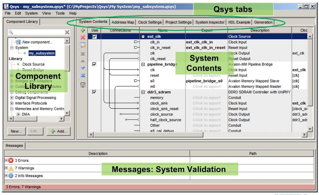
22 Qsys UI
23 System Level Design: Why Use Qsys Avoids manually developing custom interconnect fabrics and signaling. Instead of cycle-to-cycle coordination between every individual IP core, focus on transaction-level designs. Design IP without knowing exactly when data will transfer and instead only focus on how (once it does). (Only valid if you design your individual components to one of the standardized interfaces)

24 Qsys-based Method of Design
25 Connecting IP Cores
26 Interface Types Memory-mapped Interfaces: Avalon MM (Altera) AXI (ARM, supported by Qsys now for SoC) Streaming Interfaces: Avalon ST: Avalon ST source port: outputs streaming data Avalon ST sink port: receives incoming streaming data
27 Control vs. Data Planes Control Plane: Memory mapped registers typically used for configuring devices, querying status, initiating transactions, etc (low bandwidth) Data Plane: Streaming directed graphs for actually moving and processing large amounts of data (audio/video, network packets, etc); high bandwidth A single IP core can have both MM and ST interfaces (including multiple of each).
28 Control and Data Planes Example

29 Control and Data Planes Example: Solarflare AoE
30 Qsys signal types Clock Reset Interrupt Avalon MM signals (Memory-Mapped) Avalon ST signals (Streaming) Tristate Conduit (your own custom signals)
31 Why explicitly label signal types?...vs. simply making everything a wire/conduit Allows Qsys to protect you from yourself! Ensure matching between signal types (e.g., clock out clock in ) Detect and automatically insert dual clock crossing domains (only if it knows which clock domains IPs are in) Automatically convert data widths, formats, error flags (convert 32 bit master into four 8-bit slave reads, etc) Automatically synchronize and OR-gate multiple resets Automatically insert pipeline stages to improve fmax

32 Avalon MM Master Signals

33 Avalon MM Slave Signals

34 Avalon ST Signals

35 Example Qsys Layout: 10Gb Reference Design

36 Advanced: Qsys Hierarchical Designs
37 Advanced: Qsys Automatic Pipelining

38 Advanced: Qsys Testbench Generation
39 Additional References Altera online training lectures: (HIGHLY recommended; many of these slides are taken directly from them) curriculum/trn-curriculum.html Introduction to Qsys Advanced System Design Using Qsys Custom IP Development Using Avalon and AXI Interfaces
Introduction to the Qsys System Integration Tool
 Introduction to the Qsys System Integration Tool Course Description This course will teach you how to quickly build designs for Altera FPGAs using Altera s Qsys system-level integration tool. You will
Designing with ALTERA SoC Hardware
 Designing with ALTERA SoC Hardware Course Description This course provides all theoretical and practical know-how to design ALTERA SoC devices under Quartus II software. The course combines 60% theory
FPGA memory performance
 FPGA memory performance Sensor to Image GmbH Lechtorstrasse 20 D 86956 Schongau Website: www.sensor-to-image.de Email: email@sensor-to-image.de Sensor to Image GmbH Company Founded 1989 and privately owned
Designing with ALTERA SoC
 Designing with ALTERA SoC תיאורהקורס קורסזהמספקאתכלהידע התיאורטיוהמעשילתכנוןרכיביSoC שלחברתALTERA תחתסביבת הפיתוחII.Quartus הקורסמשלב 60% תיאוריהו- 40% עבודה מעשית עללוחותפיתוח.SoC הקורסמתחילבסקירתמשפחותרכבי
The Nios II Family of Configurable Soft-core Processors
 The Nios II Family of Configurable Soft-core Processors James Ball August 16, 2005 2005 Altera Corporation Agenda Nios II Introduction Configuring your CPU FPGA vs. ASIC CPU Design Instruction Set Architecture
ALTERA FPGAs Architecture & Design
 ALTERA FPGAs Architecture & Design Course Description This course provides all theoretical and practical know-how to design programmable devices of ALTERA with QUARTUS-II design software. The course combines
Advanced ALTERA FPGA Design
 Advanced ALTERA FPGA Design Course Description This course focuses on advanced FPGA design topics in Quartus software. The first part covers advanced timing closure problems, analysis and solutions. The
Applying the Benefits of Network on a Chip Architecture to FPGA System Design
 white paper Intel FPGA Applying the Benefits of on a Chip Architecture to FPGA System Design Authors Kent Orthner Senior Manager, Software and IP Intel Corporation Table of Contents Abstract...1 Introduction...1
SoC Platforms and CPU Cores
 SoC Platforms and CPU Cores COE838: Systems on Chip Design http://www.ee.ryerson.ca/~courses/coe838/ Dr. Gul N. Khan http://www.ee.ryerson.ca/~gnkhan Electrical and Computer Engineering Ryerson University
Designing with Nios II Processor for Hardware Engineers
 Designing with Nios II Processor for Hardware Engineers Course Description This course provides all theoretical and practical know-how to design ALTERA SoC FPGAs based on the Nios II soft processor under
Avalon Interface Specifications
 Avalon Interface Specifications 101 Innovation Drive San Jose, CA 95134 www.altera.com Document Version: 1.1 Document Date: October 2008 Copyright 2008 Altera Corporation. All rights reserved. Altera,
9. PIO Core. Core Overview. Functional Description
 9. PIO Core NII51007-9.0.0 Core Overview The parallel input/output (PIO) core with Avalon interface provides a memory-mapped interface between an Avalon Memory-Mapped (Avalon-MM) slave port and general-purpose
Avalon Interface Specifications
 Updated for Intel Quartus Prime Design Suite: 18.0 Subscribe Send Feedback Latest document on the web: PDF HTML Contents Contents 1. Introduction to the Avalon Interface Specifications... 4 1.1. Avalon
Creating PCI Express Links in Intel FPGAs
 Creating PCI Express Links in Intel FPGAs Course Description This course provides all necessary theoretical and practical know how to create PCI Express links in Intel FPGAs. The course goes into great
4. TriMatrix Embedded Memory Blocks in HardCopy IV Devices
 January 2011 HIV51004-2.2 4. TriMatrix Embedded Memory Blocks in HardCopy IV Devices HIV51004-2.2 This chapter describes TriMatrix memory blocks, modes, features, and design considerations in HardCopy
Avalon Interface Specifications
 Updated for Intel Quartus Prime Design Suite: 18.1 Subscribe Latest document on the web: PDF HTML Contents Contents 1. Introduction to the...4 1.1. Avalon Properties and Parameters...5 1.2. Signal Roles...5
Field Programmable Gate Array (FPGA) Devices
 Devices") Field Programmable Gate Array (FPGA) Devices 1 Contents Altera FPGAs and CPLDs CPLDs FPGAs with embedded processors ACEX FPGAs Cyclone I,II FPGAs APEX FPGAs Stratix FPGAs Stratix II,III FPGAs Xilinx FPGAs
Field Programmable Gate Array (FPGA) Devices 1 Contents Altera FPGAs and CPLDs CPLDs FPGAs with embedded processors ACEX FPGAs Cyclone I,II FPGAs APEX FPGAs Stratix FPGAs Stratix II,III FPGAs Xilinx FPGAs
Designing Embedded Processors in FPGAs
 Designing Embedded Processors in FPGAs 2002 Agenda Industrial Control Systems Concept Implementation Summary & Conclusions Industrial Control Systems Typically Low Volume Many Variations Required High
3-D Accelerator on Chip
 3-D Accelerator on Chip Third Prize 3-D Accelerator on Chip Institution: Participants: Instructor: Donga & Pusan University Young-Hee Won, Jin-Sung Park, Woo-Sung Moon Sam-Hak Jin Design Introduction Recently,
Creating a System With Qsys
 6 QII51020 Subscribe Qsys is a system integration tool included as part of the Quartus II software. Qsys captures system-level hardware designs at a high level of abstraction and automates the task of
FPGA for Software Engineers
 FPGA for Software Engineers Course Description This course closes the gap between hardware and software engineers by providing the software engineer all the necessary FPGA concepts and terms. The course
SoC FPGAs. Your User-Customizable System on Chip Altera Corporation Public
 SoC FPGAs Your User-Customizable System on Chip Embedded Developers Needs Low High Increase system performance Reduce system power Reduce board size Reduce system cost 2 Providing the Best of Both Worlds
Section III. Transport and Communication
 Section III. Transport and Communication This section describes communication and transport peripherals provided for SOPC Builder systems. This section includes the following chapters: Chapter 16, SPI
Creating a System With Qsys
 5 QII51020 Subscribe Qsys is a system integration tool included as part of the Quartus II software. Qsys captures system-level hardware designs at a high level of abstraction and simplifies the task of
Design of Embedded Hardware and Firmware
 Design of Embedded Hardware and Firmware Introduction on "System On Programmable Chip" NIOS II Avalon Bus - DMA Andres Upegui Laboratoire de Systèmes Numériques hepia/hes-so Geneva, Switzerland Embedded
Digital Systems Design
 Digital Systems Design Custom Components for NIOS II Systems Dr. D. J. Jackson Lecture 15-1 Qsys Components A Qsys component includes the following elements: Information about the component type, such
COSC 243. Computer Architecture 1. COSC 243 (Computer Architecture) Lecture 6 - Computer Architecture 1 1
 Lecture 6 - Computer Architecture 1 1") COSC 243 Computer Architecture 1 COSC 243 (Computer Architecture) Lecture 6 - Computer Architecture 1 1 Overview Last Lecture Flip flops This Lecture Computers Next Lecture Instruction sets and addressing
COSC 243 Computer Architecture 1 COSC 243 (Computer Architecture) Lecture 6 - Computer Architecture 1 1 Overview Last Lecture Flip flops This Lecture Computers Next Lecture Instruction sets and addressing
System-on Solution from Altera and Xilinx
 System-on on-a-programmable-chip Solution from Altera and Xilinx Xun Yang VLSI CAD Lab, Computer Science Department, UCLA FPGAs with Embedded Microprocessors Combination of embedded processors and programmable
PCI Express Multi-Channel DMA Interface
 2014.12.15 UG-01160 Subscribe The PCI Express DMA Multi-Channel Controller Example Design provides multi-channel support for the Stratix V Avalon Memory-Mapped (Avalon-MM) DMA for PCI Express IP Core.
2. System Interconnect Fabric for Memory-Mapped Interfaces
 2. System Interconnect Fabric for Memory-Mapped Interfaces QII54003-8.1.0 Introduction The system interconnect fabric for memory-mapped interfaces is a high-bandwidth interconnect structure for connecting
Nios II Embedded Design Suite Release Notes
 Nios II Embedded Design Suite Release Notes Subscribe Send Feedback Latest document on the web: PDF HTML Contents Contents 1...3 1.1 Product Revision History... 3 1.2 Nios II EDS v15.0 Updates...4 1.3
9. Building Memory Subsystems Using SOPC Builder
 9. Building Memory Subsystems Using SOPC Builder QII54006-6.0.0 Introduction Most systems generated with SOPC Builder require memory. For example, embedded processor systems require memory for software
ALTERA FPGA Design Using Verilog
 ALTERA FPGA Design Using Verilog Course Description This course provides all necessary theoretical and practical know-how to design ALTERA FPGA/CPLD using Verilog standard language. The course intention
Cover TBD. intel Quartus prime Design software
 Cover TBD intel Quartus prime Design software Fastest Path to Your Design The Intel Quartus Prime software is revolutionary in performance and productivity for FPGA, CPLD, and SoC designs, providing a
«Real Time Embedded systems» Cyclone V SOC - FPGA
 «Real Time Embedded systems» Cyclone V SOC - FPGA Ref: http://www.altera.com rene.beuchat@epfl.ch LAP/ISIM/IC/EPFL Chargé de cours rene.beuchat@hesge.ch LSN/hepia Prof. HES 1 SOC + FPGA (ex. Cyclone V,
Copyright 2016 Xilinx
 Zynq Architecture Zynq Vivado 2015.4 Version This material exempt per Department of Commerce license exception TSU Objectives After completing this module, you will be able to: Identify the basic building
Zynq-7000 All Programmable SoC Product Overview
 Zynq-7000 All Programmable SoC Product Overview The SW, HW and IO Programmable Platform August 2012 Copyright 2012 2009 Xilinx Introducing the Zynq -7000 All Programmable SoC Breakthrough Processing Platform
SEMICON Solutions. Bus Structure. Created by: Duong Dang Date: 20 th Oct,2010
 SEMICON Solutions Bus Structure Created by: Duong Dang Date: 20 th Oct,2010 Introduction Buses are the simplest and most widely used interconnection networks A number of modules is connected via a single
BlazePPS (Blaze Packet Processing System) CSEE W4840 Project Design
 CSEE W4840 Project Design") BlazePPS (Blaze Packet Processing System) CSEE W4840 Project Design Valeh Valiollahpour Amiri (vv2252) Christopher Campbell (cc3769) Yuanpei Zhang (yz2727) Sheng Qian ( sq2168) March 26, 2015 I) Hardware
BlazePPS (Blaze Packet Processing System) CSEE W4840 Project Design Valeh Valiollahpour Amiri (vv2252) Christopher Campbell (cc3769) Yuanpei Zhang (yz2727) Sheng Qian ( sq2168) March 26, 2015 I) Hardware
Avalon Interface. Avalon Interfaces. Open Standard. 7 Interfaces. Streaming Memory Mapped Conduit Tri-state Conduit Interrupt Clock Reset
 Avalon Interfaces Open Standard 7 Interfaces Streaming Memory Mapped Conduit Tri-state Conduit Interrupt Clock Reset 2 tj Avalon Interfaces Each interface can include Properties and Parameters Signals
Buses. Maurizio Palesi. Maurizio Palesi 1
 Buses Maurizio Palesi Maurizio Palesi 1 Introduction Buses are the simplest and most widely used interconnection networks A number of modules is connected via a single shared channel Microcontroller Microcontroller
Altera FLEX 8000 Block Diagram
 Altera FLEX 8000 Block Diagram Figure from Altera technical literature FLEX 8000 chip contains 26 162 LABs Each LAB contains 8 Logic Elements (LEs), so a chip contains 208 1296 LEs, totaling 2,500 16,000
DDR and DDR2 SDRAM Controller Compiler User Guide
 DDR and DDR2 SDRAM Controller Compiler User Guide 101 Innovation Drive San Jose, CA 95134 www.altera.com Operations Part Number Compiler Version: 8.1 Document Date: November 2008 Copyright 2008 Altera
Cover TBD. intel Quartus prime Design software
 Cover TBD intel Quartus prime Design software Fastest Path to Your Design The Intel Quartus Prime software is revolutionary in performance and productivity for FPGA, CPLD, and SoC designs, providing a
SoC Design Lecture 11: SoC Bus Architectures. Shaahin Hessabi Department of Computer Engineering Sharif University of Technology
 SoC Design Lecture 11: SoC Bus Architectures Shaahin Hessabi Department of Computer Engineering Sharif University of Technology On-Chip bus topologies Shared bus: Several masters and slaves connected to
4. Functional Description HPS Memory Controller
 November 2012 EMI_RM_017-1.0 4. Functional Description HPS Memory Controller EMI_RM_017-1.0 The hard processor system (HPS) SDRAM controller subsystem provides efficient access to external SDRAM for the
The simplest form of storage is a register file. All microprocessors have register files, which are known as registers in the architectural context.
 1 In this lecture, we will consider the various type of storage (memory) that FPGAs allow us to implement. The major advantage of FPGAs is that it contains lots of small blocks of memory modules, which
Cornell Cup Tutorials
 Cornell Cup Tutorials Online Tutorials Atom processor FPGA material Yocto tools 2 Atom processor For N2600 (CedarView) information: Based on 32nm process technology, the processor series feature new levels
Getting Started With the Nios II DPX Datapath Processor ---Version
 Getting Started With the Nios II DPX Datapath Processor ---Version 11.0--- This tutorial teaches you how to develop a complete system employing Altera event-driven datapath processing. In this tutorial,
Nios Soft Core Embedded Processor
 Nios Soft Core Embedded Processor June 2000, ver. 1 Data Sheet Features... Preliminary Information Part of Altera s Excalibur TM embedded processor solutions, the Nios TM soft core embedded processor is
Digital Blocks Semiconductor IP
 Digital Blocks Semiconductor IP General Description The Digital Blocks LCD Controller IP Core interfaces a video image in frame buffer memory via the AMBA 3.0 / 4.0 AXI Protocol Interconnect to a 4K and
SoC Design. Prof. Dr. Christophe Bobda Institut für Informatik Lehrstuhl für Technische Informatik
 SoC Design Prof. Dr. Christophe Bobda Institut für Informatik Lehrstuhl für Technische Informatik Chapter 5 On-Chip Communication Outline 1. Introduction 2. Shared media 3. Switched media 4. Network on
INTRODUCTION TO FIELD PROGRAMMABLE GATE ARRAYS (FPGAS)
") INTRODUCTION TO FIELD PROGRAMMABLE GATE ARRAYS (FPGAS) Bill Jason P. Tomas Dept. of Electrical and Computer Engineering University of Nevada Las Vegas FIELD PROGRAMMABLE ARRAYS Dominant digital design
INTRODUCTION TO FIELD PROGRAMMABLE GATE ARRAYS (FPGAS) Bill Jason P. Tomas Dept. of Electrical and Computer Engineering University of Nevada Las Vegas FIELD PROGRAMMABLE ARRAYS Dominant digital design
Buses. Disks PCI RDRAM RDRAM LAN. Some slides adapted from lecture by David Culler. Pentium 4 Processor. Memory Controller Hub.
 es > 100 MB/sec Pentium 4 Processor L1 and L2 caches Some slides adapted from lecture by David Culler 3.2 GB/sec Display Memory Controller Hub RDRAM RDRAM Dual Ultra ATA/100 24 Mbit/sec Disks LAN I/O Controller
Laboratory Exercise 5
 Laboratory Exercise 5 Bus Communication The purpose of this exercise is to learn how to communicate using a bus. In the designs generated by using Altera s SOPC Builder, the Nios II processor connects
MICROTRONIX AVALON MULTI-PORT FRONT END IP CORE
 MICROTRONIX AVALON MULTI-PORT FRONT END IP CORE USER MANUAL V1.0 Microtronix Datacom Ltd 126-4056 Meadowbrook Drive London, ON, Canada N5L 1E3 www.microtronix.com Document Revision History This user guide
Stratix. High-Density, High-Performance FPGAs. Available in Production Quantities
 Stratix High-Density, High-Performance FPGAs Available in Production Quantities February 2004 High-Density, High-Performance FPGAs Altera s award-winning Stratix FPGA family delivers the most comprehensive
4K Format Conversion Reference Design
 4K Format Conversion Reference Design AN-646 Application Note This application note describes a 4K format conversion reference design. 4K resolution is the next major enhancement in video because of the
8. Migrating Stratix II Device Resources to HardCopy II Devices
 8. Migrating Stratix II Device Resources to HardCopy II Devices H51024-1.3 Introduction Altera HardCopy II devices and Stratix II devices are both manufactured on a 1.2-V, 90-nm process technology and
Basic FPGA Architectures. Actel FPGAs. PLD Technologies: Antifuse. 3 Digital Systems Implementation Programmable Logic Devices
 3 Digital Systems Implementation Programmable Logic Devices Basic FPGA Architectures Why Programmable Logic Devices (PLDs)? Low cost, low risk way of implementing digital circuits as application specific
Embedded Design Handbook
 Subscribe Send Feedback Latest document on the web: PDF HTML Contents Contents 1 Introduction... 6 1.1 Document Revision History... 6 2 First Time Designer's Guide... 7 2.1 FPGAs and Soft-Core Processors...
The RM9150 and the Fast Device Bus High Speed Interconnect
 The RM9150 and the Fast Device High Speed Interconnect John R. Kinsel Principal Engineer www.pmc -sierra.com 1 August 2004 Agenda CPU-based SOC Design Challenges Fast Device (FDB) Overview Generic Device
Building Gigabit Interfaces in Altera Transceiver Devices
 Building Gigabit Interfaces in Altera Transceiver Devices Course Description In this course, you will learn how you can build high-speed, gigabit interfaces using the 28- nm embedded transceivers found
Digital Integrated Circuits
 Digital Integrated Circuits Lecture 9 Jaeyong Chung Robust Systems Laboratory Incheon National University DIGITAL DESIGN FLOW Chung EPC6055 2 FPGA vs. ASIC FPGA (A programmable Logic Device) Faster time-to-market
1. Overview for the Arria V Device Family
 1. Overview for the Arria V Device Family December 2011 AV51001-1.2 AV51001-1.2 Built on the 28-nm low-power process technology, Arria V devices offer the lowest power and lowest system cost for mainstream
Today. Comments about assignment Max 1/T (skew = 0) Max clock skew? Comments about assignment 3 ASICs and Programmable logic Others courses
 Max clock skew? Comments about assignment 3 ASICs and Programmable logic Others courses") Today Comments about assignment 3-43 Comments about assignment 3 ASICs and Programmable logic Others courses octor Per should show up in the end of the lecture Mealy machines can not be coded in a single
Today Comments about assignment 3-43 Comments about assignment 3 ASICs and Programmable logic Others courses octor Per should show up in the end of the lecture Mealy machines can not be coded in a single
Chapter 2. Cyclone II Architecture
 Chapter 2. Cyclone II Architecture CII51002-1.0 Functional Description Cyclone II devices contain a two-dimensional row- and column-based architecture to implement custom logic. Column and row interconnects
1. SDRAM Controller Core
 1. SDRAM Controller Core NII51005-7.2.0 Core Overview The SDRAM controller core with Avalon interface provides an Avalon Memory-Mapped (Avalon-MM) interface to off-chip SDRAM. The SDRAM controller allows
Hardware Design. University of Pannonia Dept. Of Electrical Engineering and Information Systems. MicroBlaze v.8.10 / v.8.20
 University of Pannonia Dept. Of Electrical Engineering and Information Systems Hardware Design MicroBlaze v.8.10 / v.8.20 Instructor: Zsolt Vörösházi, PhD. This material exempt per Department of Commerce
CONTACT: ,
 S.N0 Project Title Year of publication of IEEE base paper 1 Design of a high security Sha-3 keccak algorithm 2012 2 Error correcting unordered codes for asynchronous communication 2012 3 Low power multipliers
Functional Description HPS Memory Controller
 .. emi_rm_ Subscribe The hard processor system (HPS) SDRAM controller subsystem provides efficient access to external SDRAM for the ARM Cortex -A microprocessor unit (MPU) subsystem, the level (L) interconnect,
UG0850 User Guide PolarFire FPGA Video Solution
 UG0850 User Guide PolarFire FPGA Video Solution Microsemi Headquarters One Enterprise, Aliso Viejo, CA 92656 USA Within the USA: +1 (800) 713-4113 Outside the USA: +1 (949) 380-6100 Sales: +1 (949) 380-6136
Five Ways to Build Flexibility into Industrial Applications with FPGAs
 GM/M/A\ANNETTE\2015\06\wp-01154- flexible-industrial.docx Five Ways to Build Flexibility into Industrial Applications with FPGAs by Jason Chiang and Stefano Zammattio, Altera Corporation WP-01154-2.0 White
10-Gbps Ethernet Hardware Demonstration Reference Design
 10-Gbps Ethernet Hardware Demonstration Reference Design July 2009 AN-588-1.0 Introduction This reference design demonstrates wire-speed operation of the Altera 10-Gbps Ethernet (10GbE) reference design
Low Power Design Techniques
 Low Power Design Techniques August 2005, ver 1.0 Application Note 401 Introduction This application note provides low-power logic design techniques for Stratix II and Cyclone II devices. These devices
External Memory Interfaces in Cyclone V Devices
 External Memory Interfaces in Cyclone V Devices..8 CV-5 Subscribe Feedback The Cyclone V devices provide an efficient architecture that allows you fit wide external memory interfaces support a high level
NIOS CPU Based Embedded Computer System on Programmable Chip
 NIOS CPU Based Embedded Computer System on Programmable Chip 1 Lab Objectives EE8205: Embedded Computer Systems NIOS-II SoPC: PART-I This lab has been constructed to introduce the development of dedicated
ReNoC: A Network-on-Chip Architecture with Reconfigurable Topology
 1 ReNoC: A Network-on-Chip Architecture with Reconfigurable Topology Mikkel B. Stensgaard and Jens Sparsø Technical University of Denmark Technical University of Denmark Outline 2 Motivation ReNoC Basic
Digital Blocks Semiconductor IP
 Digital Blocks Semiconductor IP -UHD General Description The Digital Blocks -UHD LCD Controller IP Core interfaces a video image in frame buffer memory via the AMBA 3.0 / 4.0 AXI Protocol Interconnect
Excalibur Device Overview
 May 2002, ver. 2.0 Data Sheet Features... Combination of a world-class RISC processor system with industryleading programmable logic on a single device Industry-standard ARM922T 32-bit RISC processor core
Nios II Performance Benchmarks
 Subscribe Performance Benchmarks Overview This datasheet lists the performance and logic element (LE) usage for the Nios II Classic and Nios II Gen2 soft processor, and peripherals. Nios II is configurable
The Xilinx XC6200 chip, the software tools and the board development tools
 The Xilinx XC6200 chip, the software tools and the board development tools What is an FPGA? Field Programmable Gate Array Fully programmable alternative to a customized chip Used to implement functions
Section I. Cyclone II Device Family Data Sheet
 Section I. Cyclone II Device Family Data Sheet This section provides provides information for board layout designers to successfully layout their boards for Cyclone II devices. It contains the required
Altera Product Overview. Altera Product Overview
 Altera Product Overview Tim Colleran Vice President, Product Marketing Altera Product Overview High Density + High Bandwidth I/O Programmable ASSP with CDR High-Speed Product Term Embedded Processor High
Design and Implementation of Low Complexity Router for 2D Mesh Topology using FPGA
 Design and Implementation of Low Complexity Router for 2D Mesh Topology using FPGA Maheswari Murali * and Seetharaman Gopalakrishnan # * Assistant professor, J. J. College of Engineering and Technology,
SerialLite III Streaming IP Core Design Example User Guide for Intel Stratix 10 Devices
 SerialLite III Streaming IP Core Design Example User Guide for Intel Stratix 10 Devices Updated for Intel Quartus Prime Design Suite: 17.1 Stratix 10 ES Editions Subscribe Send Feedback Latest document
Chapter 6 Storage and Other I/O Topics
 Department of Electr rical Eng ineering, Chapter 6 Storage and Other I/O Topics 王振傑 (Chen-Chieh Wang) ccwang@mail.ee.ncku.edu.tw ncku edu Feng-Chia Unive ersity Outline 6.1 Introduction 6.2 Dependability,
Arria 10 Transceiver PHY User Guide
 Arria 10 Transceiver PHY User Guide Subscribe UG-A10XCVR 101 Innovation Drive San Jose, CA 95134 www.altera.com TOC-2 Arria 10 Transceiver PHY User Guide Contents Arria 10 Transceiver PHY Overview...1-1
Interconnects, Memory, GPIO
 Interconnects, Memory, GPIO Dr. Francesco Conti f.conti@unibo.it Slide contributions adapted from STMicroelectronics and from Dr. Michele Magno, others Processor vs. MCU Pipeline Harvard architecture Separate
4DM4 Lab. #1 A: Introduction to VHDL and FPGAs B: An Unbuffered Crossbar Switch (posted Thursday, Sept 19, 2013)
") 1 4DM4 Lab. #1 A: Introduction to VHDL and FPGAs B: An Unbuffered Crossbar Switch (posted Thursday, Sept 19, 2013) Lab #1: ITB Room 157, Thurs. and Fridays, 2:30-5:20, EOW Demos to TA: Thurs, Fri, Sept.
1 4DM4 Lab. #1 A: Introduction to VHDL and FPGAs B: An Unbuffered Crossbar Switch (posted Thursday, Sept 19, 2013) Lab #1: ITB Room 157, Thurs. and Fridays, 2:30-5:20, EOW Demos to TA: Thurs, Fri, Sept.
MAX 10 FPGA Device Overview
 2014.09.22 M10-OVERVIEW Subscribe MAX 10 devices are the industry s first single chip, non-volatile programmable logic devices (PLDs) to integrate the optimal set of system components. The following lists
discrete logic do not
 Welcome to my second year course on Digital Electronics. You will find that the slides are supported by notes embedded with the Powerpoint presentations. All my teaching materials are also available on
AN 830: Intel FPGA Triple-Speed Ethernet and On-Board PHY Chip Reference Design
 AN 830: Intel FPGA Triple-Speed Ethernet and On-Board PHY Chip Reference Subscribe Latest document on the web: PDF HTML Contents Contents 1. Intel FPGA Triple-Speed Ethernet and On-Board PHY Chip Reference
Hardware Design of a Flight Control Computer System based on Multi-core Digital Signal Processor and Field Programmable Gate Array
 Article Hardware Design of a Flight Control Computer System based on Multi-core Digital Signal Processor and Field Programmable Gate Array Francisco Bilendo 1 ; *francisco-bilendo@hotmail.com Sheng Shouzhao
Today s Agenda Background/Experience Course Information Altera DE2B Board do Overview Introduction to Embedded Systems Design Abstraction Microprocess
 ECEN 4633/5633 Hybrid Embedded Systems Fall 2010 Semester Dr. David Ward Today s Agenda Background/Experience Course Information Altera DE2B Board do Overview Introduction to Embedded Systems Design Abstraction
AN 830: Intel FPGA Triple-Speed Ethernet and On-Board PHY Chip Reference Design
 AN 830: Intel FPGA Triple-Speed Ethernet and On-Board PHY Chip Reference Design Subscribe Send Feedback Latest document on the web: PDF HTML Contents Contents 1 Intel FPGA Triple-Speed Ethernet and On-Board
HARDWARE SECURITY. EEC 492/592, CIS 493 Hands-on Experience on Computer System Security Chan Yu Cleveland State University
 HARDWARE SECURITY EEC 492/592, CIS 493 Hands-on Experience on Computer System Security Chan Yu Cleveland State University CONTENTS Overview of Hardware security Basics FPGA (Field Programmable Gate Array)
Digital Systems Design. System on a Programmable Chip
 Digital Systems Design Introduction to System on a Programmable Chip Dr. D. J. Jackson Lecture 11-1 System on a Programmable Chip Generally involves utilization of a large FPGA Large number of logic elements
Programmable Logic. Any other approaches?
 Programmable Logic So far, have only talked about PALs (see 22V10 figure next page). What is the next step in the evolution of PLDs? More gates! How do we get more gates? We could put several PALs on one
Simplify System Complexity
 Simplify System Complexity With the new high-performance CompactRIO controller Fanie Coetzer Field Sales Engineer Northern South Africa 2 3 New control system CompactPCI MMI/Sequencing/Logging FieldPoint