Basic System Memory Architecture View (Functional)
|
|
|
- Marilyn Anis Gregory
- 5 years ago
- Views:
Transcription
1 Memory Organization
2 Basic System Memory Architecture View (Functional) Notation: [FFFE]=27h FFFE: 27
3 Basic Characteristics (1/3) Memory cell registers are one byte wide Memory Word is the contents of the cell, usually in hex notation. Data wider than one byte uses two or more memory cells. Reading or writing memory words is done through the Data Bus
4 Basic Characteristics (2/3) Each memorycell is identified by an address The address is independent from contents! The CPU can read/write the memory cell only if the Address Bus has the address of the cell The address of the cell is a physical address Notation: To indicate the contents of a memory cell we write [addr] = contents (for ex: [0200h] = 8Ah) Unless indicated otherwise, hex notation is used ( [0200]=8A ) Memory segment: A set of memory cells with contiguous addresses.
5 Basic Characteristics (3/3) The Control Bus carries signals that are used to indicate what type of transactions are done with memory, if transaction is done with memory and so on
6 Memory Types (1/3) Classification Classified according to Storage permanence: how long data is maintained Write ability: data can be written at normal running voltage and speed conditions Storage permanence classes: Volatile memory: looses its contents when power is removed Non volatile memory: does not loose its contents when power is removed
7 Memory Types (2/3): Volatility Non volatile Examples: ROM structures: ROM, OPROM, EPROM, EEPROM Ferro Electric RAM (FRAM, FeRAM) Flash Memory Vltil Volatile Examples Static RAM (SRAM) Dynamic RAM (DRAM) Popular non volatile in MCU: Flash, FRAM
8 Memory Types (3/3): Write ability Non writable Examples: ROM structures: ROM, OPROM, EPROM, EEPROM Flash Writable Examples Static RAM (SRAM) Dynamic RAM (DRAM) FRAM FRAM memory has both non volatility and write ability
9 Comments on memory RAM (Random Access Memory) is usually used as a generic term to refer to writable and volatile memory The term ROM (Read Only Memory) is used as a generic term to refer to non writable and nonvolatile memory independently of the truthness Modern non writable memory is in fact writable, but at dff different voltages generated internally, and at slower speeds
10 More memory concepts: Physical and Data address. (1) Unless otherwise noted, memorywords will be onebyte size. Physical Address: Address of a memory cell Data size dictates how many memory words are required: 1 to 8 bits: 1 memory word 9 to 16 bits: 2 memory words Data is stored in contiguous memory cells. DATA Address: The lowest physical address of the cells occupied by data.
11 More memory concepts: Physical and Data address. (2) DATA Address: The lowest physical address of the cells occupied by data. Example 1: For data address 0F208 for 456F, physical addresses are 0F208 and 0F209. Example 2: For data address 0F208 for 456FA2B1, physical addresses are 0F208, 0F209, 0F20A, and 0F20B Notation: ti In diagrams and figures, as well as notation, ti cells may be shown in byte, word, double word sizes. Examples: 0F208: 2A or [F208] = 2A 0F208: 2AB9 or [F208] = 2AB9 0F208: 2F1A40CD or [F208] = 2F1A40CD
12 Little endian vs. big endian (1) Little endian: The data address points to the least significant byte of data (i.e., LSB in lowest physical address) Big endian: The data address points to the most significant byte of data (i.e., MSB in lowest physical address) [4300]=342B Little endian: [4300]= 2B, [4301]= 34 Big endian: [4300]= 34, [4301]= 2B

13 IAR Memory Window (1) To open Memory Window Memory Window
14 IAR Memory Window (2) To examine specific Address Zone Memory menu Use memory menu to select views byte (1x) word d(2 (2x) double word (4x) Little Endian or Big Endian Address of first byte in row (In HEX) Sixteen bytes per row ASCII value when present
15 IAR Memory Window (2) (word and double word views) Word view (Little endian) Double word view (Little endian)
16 Program and Data memory Data memory is used for storing variables and data expected to change during program execution. Program memory is used to store system programs and data that will not change during program execution and should not be lost when power is removed


17 Von Neumann and Harvard architectures Von Neumann (Princeton) architecture: Programand and data Memories share the system buses Example: MSP430, 68HC11, Intel 80x86/Pentium Harvard Architecture: Program and data storage have different memory spaces, different buses. Example: PIC MCU, Intel 8051, Atmel
18 Memory Map Memory Map: model representation of the usage given to the addressable space Example: A global Map
19 Example of a partial map: Memory Map (2)
20 CPU and Memory Hardware connection MEMORY INTERFACE
21 Basic considerations Hardware wise, the memory is distributed in banks. Usually, these banks constitute a set of byte registers (virtually or actually) The outputs of these registers are connected via internal buses to the Data Bus. The selection of a particularregister register isdone through terminals connected to the address bus. Interfacing consists in connecting the banks to the Interfacing consists in connecting the banks to the Data, Address and Control buses so that transactions can be made by the CPU
22 Basic Functional description of a bank A(n-1) A(n-2) A0 Internal Address Decoder Y(2 n-2 ) ---- Y0 word 2^(n 1) word 2^(n 2) Word 0 Read/ wr rite Routin ng Q7 Q6 Q5 Q4 Q3 Q2 Q1 Q0 CS Write Read
23 Example: ATMEL AT28C256 32KB (256 Kbits) EEPROM t /I /d df Pin Name A0 A14 Function Addresses CE OE WE Chip Enable Output Enable Write Enable I/O0 I/O7 Data Inputs/Outputs NC DC No Connect Don t Connect
24 Extract from Data sheet (1) Block Diagram
25 Extract from Data sheet (2) Operating Modes
26 Interface Principles for 8 bit Data bus systems Theeight eight IOoutputs of each bank areconnected to the Data Bus in the ordered sequence IO0 with D0, IO1 to D1, etc. For each bank the Address bus bits, are divided in two disjoint subsets: One subset directed toward the selection of internal registers One subset bsetin charge of activating ating the bank using an address decoder for the bank
27 Basics of memory interfacing ADDRESS BUS N>M BITS Memory Chip M bits from Address Bus A0 IO 0 A1 IO IO 7 DATA BUS N-M bits from Address Bus Signals from Control Bus Address Decoder.. A(M-1) CE
28 Basic Analysis Procedure Determine the combination of address bus bits that activates the bank. This set is fixed for all addresses in the space covered by the bank. Vary the set of Address Bus Bits that determine the bank s internal address from from to 11 1 to establish the set of addresses If this set is a least significant group, then the bank covers a segment Do this for each bank. The set of banks may or may Do this for each bank. The set of banks may or may not define a segment.
29 Analysis Examples on Blackboard.
30 Basic design Procedure (Data bus 8 bits) (1/2) Specify an appropriate segment or set of addresses to be covered by the bank Select the set of Address Bus Bits that will determine the bank s internal address as they change from to 11 1 Usually, this set is the least significant group, If there are many banks involved, select the group of bits that will discriminate among banks The rest of the bits are used to activate the whole set of banks.
31 Basic design Procedure (Data bus 8 bits) (1/2) An alternative and easy procedure is tu use programmable PLA or ROM s as address decoders for banks
32 Design examples on blackboard
33 Interface Principles for 16 bit Data bus systems Two banks are needed to connect to the 16 bits of bus. They work by pairs One bank is connected to least significant byte, the other to the most significant ifi tbt byte A) IO0 with D0, IO1 to D1, IO7 to D7. B) IO0 with D8, IO1 to D9. IO7 to D15 Which one goes to the LSB will determine little or big endianess. One bank of the pair works with even addresses (AD. Bus A0=0) and the other withodd addresses (A0=1) The control bus has a signal the indicates if we work with a bank only (byte operation) or with the pair (word operation)
34 Memory Interfacing (Data bus width 16 bits) Note: This is a little endian scheme ADDR. B US: AK A1 High Bank (Odd address) A0 * * A(K-1) CE IO 0 * * IO 7 Dat ta bus: D15 D8 ADDR. B US: AK A1 Low Bank (Even address) A0 * * A(K-1) CE IO 0 * * IO 7 Da ata bus: D7 D0 (A0=1) (A0 = 0) ADDR. Bus A0 ADDR. Bus A(N-1) A(K+1) ADDRESS DECODER Control Bus Signals
35 Basic Principles for 16 bit Data bus (explained with 2KB banks) Internal Addresses established with AD. Bus bits A11 A10 A2 A1 123FF 123FD ******* ******* FF 7FE **** **** Odd address 123FE 123FC ******* ******* Addresses seen by system 7FF 7FE **** **** Even address Address Decoder Operation: 1. If byte data and A0 = 0, activate even address bank only. 2. If byte data and A0 = 1, activate odd address bank only. 3. If word data, activate both banks Note: Connection to data bus determines endianness


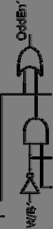
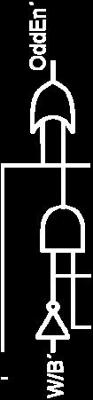
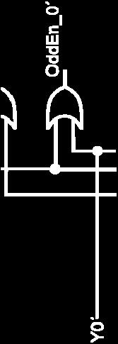
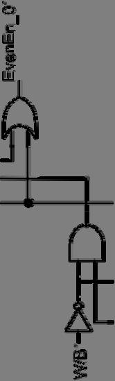
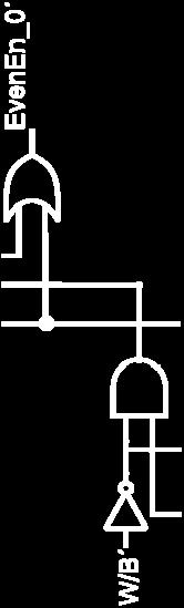
36 An example : discriminating among banks in one pair Use the previous criteria, adding an active low signal Y to select the system: Y is low, the banks are used and selected according to criteria. If Y = 1, the Modules cannot be enabled. Inputs to the system: A0, Y and W/B (1 if word, 0 if byte) Outputs: OddEn, EvenEn both active low Y W/B A0 OddEnn EvenEn X X 1 1 OddEn ' = Y ' + A0 W / B' EvenEn = Y '+ A0 W / B Note: Y is controlled by other address bus bits and/or control bus bits
37

38


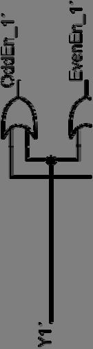
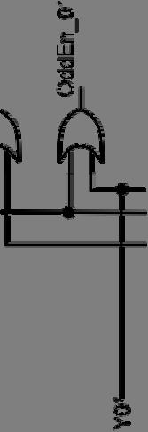
39 And for several pairs. Y0 and Y1 may be, for example, outputs of an active low decoder..
40 EXAMPLES ON BLACKBOARD
41 IO Subsystem IV Ports and peripherals
42 IO Subsystem (1) All devices connected to the system buses, other than memory and CPU Input and output ports (I/O): interface CPU with external world directly Input port Output port Input/Output port Peripherals: May be only internal to system or may have also external connection
43 IO Subsystem (2) Input transaction: Information toward CPU Output transaction: Information from CPU Important (not exhaustive) peripherals: Timers: Uses such as measuring time intervals between two events, generate interrupts at specified and many others. Wthd Watchdog Timer (WDT): Sft Safety device and/or timer ADC and DAC: to deal with analog inputs/outputs.
44 IO Structure Data Registers: Input and Output Control Registers: Used for I/O and peripheral configuration Status registers: Show information about information transfer or configuration status Control registers may contain status bits.
45 IO Mapped vs. Memory Mapped IO Mapped IO - Different sets of addresses - Different instructions for transfers Memory Mapped IO - Same system of addresses - Same instructions for transfers
46 IO Mapped vs Memory Mapped (2) IO mapped I/O has different sets of addresses for memory and for I/O subsystem CPU distinguishes address with type of instruction Example: 8086 uses MOV for transfers to/from memory, OUT to transfer to Output port, and IN from port. Routing of address bus is done by control bus according to instruction. Memory mapped I/O does not distinguish between types User must know memory map (or names ).
47 IO Ports: Remarks Input port Buffered: Readable only at a given moment Latched: Readable on demand Must not be left floating Interruptible or non interruptible Output port Always Latched
48 Important Remark for Input Do not leave an input floating: If necessary use pull up or pulldown resistors Pulldown Resistor Pullup Resistor
49 Example: MSP430 General Purpose I/O ports
50 General Purpose I/O (8 bits) Named P0 to P10 a ed 0 to 0 Number of ports and available bits depends on model P1 and P2 have interrupt capability Bit independently programmable Edge selectable interrupt capability Some series have individually programmable pulldown/pull up resistors Depending on model, pins can be configured for special I/O
51 B7 B4 B3 B2 B1 B0
52 Simplified Hardware configuration: 1. Non interruptible port Data Registers C t Control Registers
53 Basic I/O Registers (1/3) Function Selection Register (PxSEL): Selects the connection for the pin, either to the port or to other peripheral(s) 0: Connected to port (default) 1: Connected to other module(s) To connect pin 12to 1.2 port (if necessary, since it is connected by default), clear bit 2 of (P1SEL) [bic.b #BIT2, &P1SEL] To connect pin 1.2 to module, set bit 2 of (P1SEL) [bis.b #BIT2, &P1SEL] Direction Register (PxDIR): Selects in or out direction function for pin 1: Output direction 0: Input tdirection (default) Example: mov.b #0xF0, &P1DIR configures pins 4 to7 as outputs and 0 to 3 as inputs
54 Basic I/O Registers (2/3) Output Register (PxOUT): to write signal to output To output the word 0x2A to port 2: (P2OUT) #2Ah [mov.b #0x2A,&P2OUT] Input Register (PxIN): Read only register Example: mov.b &P1IN, R6 transfers input to R6 Avoid writing to this register (power consumption and does nothing)
55 Multiple peripherals pins: (3/3) SeveralFunctionSelect Select Registers (PxSEL y PxSEL2 for 2xx family): For example, in 2xx family PxSEL PxSEL2: 00: I/O pin 01: Primary peripheral module 10: Reserved (device specific) 11: Secondaryperipheral module Consult data sheets and user guides for specific information.
56 More Examples: To put pins 0, 1 and 6 of Port 3 in output mode and all the others as input: (P3DIR) # b [ mov.b #0x43,&P3DIR] To put pins 0, 1 and 6 of Port t3 in output tmode leaving the others unchanged: (P3DIR) # 0x43 OR (P3DIR) [ bis.b b #0x43,&P3DIR ] To check status (high or low) or the input at pin 3 of input port 2: Test bit 3 of port 2 [bit.b #BIT3,&P2IN]
57 Interruptible I/O ports (P1 and P2) Each pin has individual interrupt capability which can be enabled or disabled independently of other pins. Has the same registers as non interruptible I/O ports, plus threeadditional registers (all read and write registers) Interrupt capability is lost when pin is selected for peripheral
58 Simplified Hardware Configuration: Interruptible port Control Registers Status Register
59 Interruptible Port Registers Interrupt Enable Register (PxIE): enables interrupt capability 1 enabled, 0 disabled (0 default) bis.b #BIT0, &P1IE enables interrupt capability of pin P1.0 Interrupt requests from I/O ports are maskable Interrupt tcapability is lost if pin is used for other module. Interupt Edge Select Register (PxIES): 1: high to low, 0 low to high (0 default) Interrupt Flags (PxIFG) Automatically set when interrupt is generated Writable, so interrupt may be generated by software ATTENTION: I/O IFG Reset only by software (Ex. bic.b b #BIT0,P1IF) 0: no interrupt pending, 1: interrupt pending
60 I/O Ports with Pull up Pull down Resistor (Example from MSP430g2211 data sheet. Consult specific information for other models. Diagram is not complete) PSEL PDIR Pout PREn Condition 0 0 x 0 IN, no R In, R pull down IN, pull up R Out 0 1 x 1 Illegal Use with module
61 Remarks In your launchpad: Check if R pull up is connected at P1.3 if using push button (see next slide) If not, connect with software: bic.b b #BIT3,&P1DIR ; verify input status bis.b #BIT3,&P1REN ; connect resistor and bis.b #BIT3,&P1OUT ; set it as pull up Make an habit to set unused port pins as outputs.


62 USB Connector Pull-up Resistors: R34 for user key* and R27 for reset key Left Port Header J1 Jumper Set J3 Right Port Header J2 MSP430 Optional Power Port * Note: R34 not in later versions. It must be configured internally User Key Jumper Set J5 Reset Key
6. General purpose Input/Output
 Chapter 6 6. General purpose Input/Output This chapter starts with a description of one of the simplest integrated peripherals of the MSP430 the General Purpose 8-bit Input Output (GPIO). The Input/Output
ECE2049 E17 Lecture 4 MSP430 Architecture & Intro to Digital I/O
 ECE2049-E17 Lecture 4 1 ECE2049 E17 Lecture 4 MSP430 Architecture & Intro to Digital I/O Administrivia Homework 1: Due today by 7pm o Either place in box in ECE office or give to me o Office hours tonight!
Topic 3. ARM Cortex M3(i) Memory Management and Access. Department of Electronics Academic Year 14/15. (ver )
 Memory Management and Access. Department of Electronics Academic Year 14/15. (ver )") Topic 3 ARM Cortex M3(i) Memory Management and Access Department of Electronics Academic Year 14/15 (ver 25-10-2014) Index 3.1. Memory maps 3.2. Memory expansion 3.3. Memory management & Data alignment
Topic 3 ARM Cortex M3(i) Memory Management and Access Department of Electronics Academic Year 14/15 (ver 25-10-2014) Index 3.1. Memory maps 3.2. Memory expansion 3.3. Memory management & Data alignment
The digital I/O is configured with user software. The setup and operation of the digital I/O is discussed in the following sections.
 Digital I/O Introduction www.ti.com 8. Digital I/O Introduction MSP43 devices have up to eight digital I/O ports implemented, P to P8. Each port has up to eight I/O pins. Every I/O pin is individually
Interconnects, Memory, GPIO
 Interconnects, Memory, GPIO Dr. Francesco Conti f.conti@unibo.it Slide contributions adapted from STMicroelectronics and from Dr. Michele Magno, others Processor vs. MCU Pipeline Harvard architecture Separate
EE251: Thursday November 15
 EE251: Thursday November 15 Major new topic: MEMORY A KEY topic HW #7 due today; HW #8 due Thursday, Nov. 29 Lab #8 finishes this week; due week of Nov. 26 All labs MUST be completed/handed-in by Dec.
Computer Hardware Requirements for ERTSs: Microprocessors & Microcontrollers
 Lecture (4) Computer Hardware Requirements for ERTSs: Microprocessors & Microcontrollers Prof. Kasim M. Al-Aubidy Philadelphia University-Jordan DERTS-MSc, 2015 Prof. Kasim Al-Aubidy 1 Lecture Outline:
Address connections Data connections Selection connections
 Interface (cont..) We have four common types of memory: Read only memory ( ROM ) Flash memory ( EEPROM ) Static Random access memory ( SARAM ) Dynamic Random access memory ( DRAM ). Pin connections common
Allmost all systems contain two main types of memory :
 Memory Interface Allmost all systems contain two main types of memory : read-only memory (ROM) system software and permanent system data random access memory (RAM) or read/write memory application software
ECE2049-E18 Lecture 6 Notes 1. ECE2049: Embedded Computing in Engineering Design E Term Lecture #6: Exam Review
 ECE2049-E18 Lecture 6 Notes 1 ECE2049: Embedded Computing in Engineering Design E Term 2018 Lecture #6: Exam Review Administrivia Exam 1: Next Tuesday (6/5) HW4: Short assignment, due Tuesday Lab 1: Due
EE 308: Microcontrollers
 EE 308: Microcontrollers AVR Architecture Aly El-Osery Electrical Engineering Department New Mexico Institute of Mining and Technology Socorro, New Mexico, USA January 23, 2018 Aly El-Osery (NMT) EE 308:
Module 2: Introduction to AVR ATmega 32 Architecture
 Module 2: Introduction to AVR ATmega 32 Architecture Definition of computer architecture processor operation CISC vs RISC von Neumann vs Harvard architecture AVR introduction AVR architecture Architecture
ECE2049: Embedded Computing in Engineering Design A Term Fall Lecture #9: Exam Review w/ Solutions
 ECE2049: Embedded Computing in Engineering Design A Term Fall 2018 Lecture #9: Exam Review w/ Solutions Reading for Today: Review all reading and notes, Davies Ch 1, 2, 4,7, MSP430 User's Guide Ch 6.1,
ECE2049 Homework #2 The MSP430 Architecture & Basic Digital IO (DUE Friday 9/8/17 at 4 pm in class)
") ECE2049 Homework #2 The MSP430 Architecture & Basic Digital IO (DUE Friday 9/8/17 at 4 pm in class) Your homework should be neat and professional looking. You will loose points if your HW is not properly
ECE2049 Homework #2 The MSP430 Architecture & Basic Digital IO (DUE Friday 9/8/17 at 4 pm in class) Your homework should be neat and professional looking. You will loose points if your HW is not properly
Block diagram of processor (Harvard)
") Block diagram of processor (Harvard) Register transfer view of Harvard architecture Separate busses for instruction memory and data memory Example: PIC 16 load path OP REG AC 16 16 store path rd wr data
Block diagram of processor (Harvard) Register transfer view of Harvard architecture Separate busses for instruction memory and data memory Example: PIC 16 load path OP REG AC 16 16 store path rd wr data
Menu. word size # of words byte = 8 bits
 Menu LSI Components >Random Access Memory (RAM) Static RAM (SRAM) Dynamic RAM (DRAM) Read-Only Memory (ROM) Look into my... See figures from Lam text on web: RAM_ROM_ch6.pdf 1 It can be thought of as 1
CHAPTER TWELVE - Memory Devices
 CHAPTER TWELVE - Memory Devices 12.1 6x1,024 = 16,384 words; 32 bits/word; 16,384x32 = 524,288 cells 12.2 16,384 addresses; one per word. 12.3 2 16 = 65,536 words = 64K. Thus, memory capacity is 64Kx4.
Introduction read-only memory random access memory
 Memory Interface Introduction Simple or complex, every microprocessorbased system has a memory system. Almost all systems contain two main types of memory: read-only memory (ROM) and random access memory
Concept of Memory. The memory of computer is broadly categories into two categories:
 Concept of Memory We have already mentioned that digital computer works on stored programmed concept introduced by Von Neumann. We use memory to store the information, which includes both program and data.
Interface DAC to a PC. Control Word of MC1480 DAC (or DAC 808) 8255 Design Example. Engineering 4862 Microprocessors
 8255 Design Example. Engineering 4862 Microprocessors") Interface DAC to a PC Engineering 4862 Microprocessors Lecture 22 Cheng Li EN-4012 licheng@engr.mun.ca DAC (Digital-to-Analog Converter) Device used to convert digital pulses to analog signals Two methods
Interface DAC to a PC Engineering 4862 Microprocessors Lecture 22 Cheng Li EN-4012 licheng@engr.mun.ca DAC (Digital-to-Analog Converter) Device used to convert digital pulses to analog signals Two methods
 Chapter 1 Microprocessor architecture ECE 3120 Dr. Mohamed Mahmoud http://iweb.tntech.edu/mmahmoud/ mmahmoud@tntech.edu Outline 1.1 Computer hardware organization 1.1.1 Number System 1.1.2 Computer hardware
Microprocessor Architecture. mywbut.com 1
 Microprocessor Architecture mywbut.com 1 Microprocessor Architecture The microprocessor can be programmed to perform functions on given data by writing specific instructions into its memory. The microprocessor
ECE2049-E17 Lecture 6 1. ECE2049: Embedded Computing in Engineering Design E Term Lecture #6: Exam Review
 ECE2049-E17 Lecture 6 1 ECE2049: Embedded Computing in Engineering Design E Term 2017 Lecture #6: Exam Review Administrivia Exam 1: Next Tuesday (6/6) HW2: Due Tonight at 7pm Lab 1: Due next Tuesday (6/6),
Memory Map for the MCU320 board:
 Memory Map for the MCU320 board: The Intel 8051 MCUs and all derivatives are based on the Harvard architecture. This is to say that they have separate memory space for program (CODE) and external data
8051 Microcontroller
 8051 Microcontroller The 8051, Motorola and PIC families are the 3 leading sellers in the microcontroller market. The 8051 microcontroller was originally developed by Intel in the late 1970 s. Today many
MicroProcessor. MicroProcessor. MicroProcessor. MicroProcessor
 1 2 A microprocessor is a single, very-large-scale-integration (VLSI) chip that contains many digital circuits that perform arithmetic, logic, communication, and control functions. When a microprocessor
IV B.Tech. I Sem (R13) ECE : Embedded Systems : UNIT -2 1 UNIT 2
 ECE : Embedded Systems : UNIT -2 1 UNIT 2") IV B.Tech. I Sem (R13) ECE : Embedded Systems : UNIT -2 1 UNIT 2 1. Block diagram of MSP430x5xx series micro-controller --------------------- 1 2. CPU architecture of MSP430x5xx ------------------------------------------------
IV B.Tech. I Sem (R13) ECE : Embedded Systems : UNIT -2 1 UNIT 2 1. Block diagram of MSP430x5xx series micro-controller --------------------- 1 2. CPU architecture of MSP430x5xx ------------------------------------------------
FIFTH SEMESTER DIPLOMA EXAMINATION IN ENGINEERING/ TECHNOLOGY-MARCH 2014 EMBEDDED SYSTEMS (Common for CT,CM) [Time: 3 hours] (Maximum marks : 100)
![FIFTH SEMESTER DIPLOMA EXAMINATION IN ENGINEERING/ TECHNOLOGY-MARCH 2014 EMBEDDED SYSTEMS (Common for CT,CM) [Time: 3 hours] (Maximum marks : 100)](/thumbs/76/73351884.jpg "FIFTH SEMESTER DIPLOMA EXAMINATION IN ENGINEERING/ TECHNOLOGY-MARCH 2014 EMBEDDED SYSTEMS (Common for CT,CM) [Time: 3 hours] (Maximum marks : 100)") (Revision-10) FIFTH SEMESTER DIPLOMA EXAMINATION IN ENGINEERING/ TECHNOLOGY-MARCH 2014 EMBEDDED SYSTEMS (Common for CT,CM) [Time: 3 hours] (Maximum marks : 100) PART-A (Maximum marks : 10) I. Answer all
(Revision-10) FIFTH SEMESTER DIPLOMA EXAMINATION IN ENGINEERING/ TECHNOLOGY-MARCH 2014 EMBEDDED SYSTEMS (Common for CT,CM) [Time: 3 hours] (Maximum marks : 100) PART-A (Maximum marks : 10) I. Answer all
Computer Hardware Requirements for Real-Time Applications
 Lecture (4) Computer Hardware Requirements for Real-Time Applications Prof. Kasim M. Al-Aubidy Computer Engineering Department Philadelphia University Real-Time Systems, Prof. Kasim Al-Aubidy 1 Lecture
Introduction to general architectures of 8 and 16 bit micro-processor and micro-controllers
 Introduction to general architectures of 8 and 16 bit micro-processor and micro-controllers A microcontroller is a microprocessor with inbuilt peripherals.a microcontroller can also be compared with a
Scope & Register Access
 Scope & Register Access Scope Scope Region of a program in which a defined object is visible Defined Objects Variables Functions Two types of regions Blocks Not in a block 2 tj Scope Program Prototype
MSP-EXP430fr5994 Experimenter Board with noforth 5994
 (jan 2018) noforth website MSP-EXP430fr5994 Experimenter Board with noforth 5994 1. MSP-EXP430fr5994 Experimenter Board with noforth 5994 i/o port connections on Experimenter Board Connectors on Experimenter
UMBC. Select. Read. Write. Output/Input-output connection. 1 (Feb. 25, 2002) Four commonly used memories: Address connection ... Dynamic RAM (DRAM)
 Four commonly used memories: Address connection ... Dynamic RAM (DRAM)") Memory Types Two basic types: ROM: Read-only memory RAM: Read-Write memory Four commonly used memories: ROM Flash (EEPROM) Static RAM (SRAM) Dynamic RAM (DRAM) Generic pin configuration: Address connection
Memory Types Two basic types: ROM: Read-only memory RAM: Read-Write memory Four commonly used memories: ROM Flash (EEPROM) Static RAM (SRAM) Dynamic RAM (DRAM) Generic pin configuration: Address connection
Lecture Objectives. Introduction to Computing Chapter 0. Topics. Numbering Systems 04/09/2017
 Lecture Objectives Introduction to Computing Chapter The AVR microcontroller and embedded systems using assembly and c Students should be able to: Convert between base and. Explain the difference between
Embedded Systems. PIC16F84A Internal Architecture. Eng. Anis Nazer First Semester
 Embedded Systems PIC16F84A Internal Architecture Eng. Anis Nazer First Semester 2017-2018 Review Computer system basic components? CPU? Memory? I/O? buses? Instruction? Program? Instruction set? CISC,
EE 308 Spring Lecture 28 March 30, 2012 Review for Exam 2. Introduction to the MC9S12 Expanded Mode
 Lecture 28 March 30, 2012 Review for Exam 2 Introduction to the MC9S12 Expanded Mode 1 Review for Exam 2 1. C Programming (a) Setting and clearing bits in registers PORTA = PORTA 0x02; PORTA = PORTA &
CHAPTER 1 MICROCOMPUTER SYSTEMS. 1.1 Introduction. 1.2 Microcontroller Evolution
 CHAPTER 1 MICROCOMPUTER SYSTEMS 1.1 Introduction The term microcomputer is used to describe a system that includes a microprocessor, program memory, data memory, and an input/output (I/O). Some microcomputer
MOTENC-Lite 4-Axis PCI Motion & I/O Control Board. Reference Manual Rev 1.1, June 20, Copyright 2005 VITAL Systems Inc
 MOTENC-Lite 4-Axis PCI Motion & I/O Control Board Reference Manual Rev 1.1, June 20, 2005 Copyright 2005 VITAL Systems Inc www.vitalsystem.com This Page Intentionally Left Blank Table of Contents 1. OVERVIEW...
EE4390 Microprocessors. Lessons 2, 3 68HC12 Hardware Overview, Subsystems, and memory System
 EE4390 Microprocessors Lessons 2, 3 68HC12 Hardware Overview, Subsystems, and memory System 1 Overview 68HC12 hardware overview Subsystems Memory System 2 68HC12 Hardware Overview "Copyright of Motorola,
AVR Microcontrollers Architecture
 ก ก There are two fundamental architectures to access memory 1. Von Neumann Architecture 2. Harvard Architecture 2 1 Harvard Architecture The term originated from the Harvard Mark 1 relay-based computer,
Read and Write Cycles
 Read and Write Cycles The read cycle is shown. Figure 41.1a. The RAS and CAS signals are activated one after the other to latch the multiplexed row and column addresses respectively applied at the multiplexed
Microcontroller systems Lec 2 PIC18LF8722 Microcontroller s s core
 TKT-3500 Microcontroller systems Lec 2 PIC18LF8722 Microcontroller s s core Erno Salminen Copyright notice Some figures by Robert Reese, from supplementary CD of the course book from PIC18F8722 Family
+1 (479)
") Memory Courtesy of Dr. Daehyun Lim@WSU, Dr. Harris@HMC, Dr. Shmuel Wimer@BIU and Dr. Choi@PSU http://csce.uark.edu +1 (479) 575-6043 yrpeng@uark.edu Memory Arrays Memory Arrays Random Access Memory Serial
Memory Courtesy of Dr. Daehyun Lim@WSU, Dr. Harris@HMC, Dr. Shmuel Wimer@BIU and Dr. Choi@PSU http://csce.uark.edu +1 (479) 575-6043 yrpeng@uark.edu Memory Arrays Memory Arrays Random Access Memory Serial
MICROPROCESSOR BASED SYSTEM DESIGN
 MICROPROCESSOR BASED SYSTEM DESIGN Lecture 5 Xmega 128 B1: Architecture MUHAMMAD AMIR YOUSAF VON NEUMAN ARCHITECTURE CPU Memory Execution unit ALU Registers Both data and instructions at the same system
CREATED BY M BILAL & Arslan Ahmad Shaad Visit:
 CREATED BY M BILAL & Arslan Ahmad Shaad Visit: www.techo786.wordpress.com Q1: Define microprocessor? Short Questions Chapter No 01 Fundamental Concepts Microprocessor is a program-controlled and semiconductor
Module I. Microcontroller can be classified on the basis of their bits processed like 8bit MC, 16bit MC.
 MICROCONTROLLERS AND APPLICATIONS 1 Module 1 Module I Introduction to Microcontrollers: Comparison with Microprocessors Harvard and Von Neumann Architectures - 80C51 microcontroller features - internal
Ali Karimpour Associate Professor Ferdowsi University of Mashhad
 AUTOMATIC CONTROL SYSTEMS Ali Karimpour Associate Professor Ferdowsi University of Mashhad Main reference: Christopher T. Kilian, (2001), Modern Control Technology: Components and Systems Publisher: Delmar
Chapter 1. Microcontroller Overview
 Chapter 1 Microcontroller Overview Lesson 2 Microcontrollers- Types and Examples Outline Microcontroller Types Examples- 8051 Series Family Members Examples- 68HC11/12 Series Family Members CPU Microcomputer
Memory & Simple I/O Interfacing
 Chapter 10 Memory & Simple I/O Interfacing Expected Outcomes Explain the importance of tri-state devices in microprocessor system Distinguish basic type of semiconductor memory and their applications Relate
Introduction to Embedded Systems
 Stefan Kowalewski, 4. November 25 Introduction to Embedded Systems Part 2: Microcontrollers. Basics 2. Structure/elements 3. Digital I/O 4. Interrupts 5. Timers/Counters Introduction to Embedded Systems
Memory Expansion. Lecture Embedded Systems
 Memory Expansion Lecture 22 22-1 In These Notes... Memory Types Memory Expansion Interfacing Parallel Serial Direct Memory Access controllers 22-2 Memory Characteristics and Issues Volatility - Does it
Microcomputer Architecture and Programming
 IUST-EE (Chapter 1) Microcomputer Architecture and Programming 1 Outline Basic Blocks of Microcomputer Typical Microcomputer Architecture The Single-Chip Microprocessor Microprocessor vs. Microcontroller
Microprocessors/Microcontrollers
 Microprocessors/Microcontrollers A central processing unit (CPU) fabricated on one or more chips, containing the basic arithmetic, logic, and control elements of a computer that are required for processing
8051 INTERFACING TO EXTERNAL MEMORY
 8051 INTERFACING TO EXTERNAL MEMORY Memory Capacity The number of bits that a semiconductor memory chip can store Called chip capacity It can be in units of Kbits (kilobits), Mbits (megabits), and so on
Systems Programming. Lecture 4 Z16 Architecture and Programming
 Systems Programming www.atomicrhubarb.com/systems Lecture 4 Z16 Architecture and Programming Section Topic Where in the books Zilog Zilog Zilog Zilog UM197 (ZNEO Z16F Series Flash Microcontroller Contest
The Microcontroller. Lecture Set 3. Major Microcontroller Families. Example Microcontroller Families Cont. Example Microcontroller Families
 The Microcontroller Lecture Set 3 Architecture of the 8051 Microcontroller Microcontrollers can be considered as self-contained systems with a processor, memory and I/O ports. In most cases, all that is
COMP2121: Microprocessors and Interfacing. Introduction to Microprocessors
 COMP2121: Microprocessors and Interfacing Introduction to Microprocessors http://www.cse.unsw.edu.au/~cs2121 Lecturer: Hui Wu Session 2, 2017 1 1 Contents Processor architectures Bus Memory hierarchy 2
Micro computer Organization
 Micro computer Organization I Base Basic Components CPU SYSTEM BUSES VDD CLK RESET 1 MPU vs MCU Microprocessor Unit (MPU) CPU (called Microprocessor) is a die All components external to die Basically on
7 8 9 C. PRELAB REQUIREMENTS You must adhere to the Lab Rules and Policies document for every lab.
 Page 1/ Revision 1 OBJECTIVES To understand how a keypad functions as a raster scan input device and to learn how to interface a keypad to a microprocessor. Further explore and understand the implementation
Chapter 2 Sections 1 8 Dr. Iyad Jafar
 Introducing the PIC 16 Series and the 16F84A Chapter 2 Sections 1 8 Dr. Iyad Jafar Outline Overview of the PIC 16 Series An Architecture Overview of the 16F84A The 16F84A Memory Organization Memory Addressing
CPE 323 MSP430 INSTRUCTION SET ARCHITECTURE (ISA)
") CPE 323 MSP430 INSTRUCTION SET ARCHITECTURE (ISA) Aleksandar Milenković Email: milenka@uah.edu Web: http://www.ece.uah.edu/~milenka Objective Introduce MSP430 Instruction Set Architecture (Class of ISA,
CPE 323 MSP430 INSTRUCTION SET ARCHITECTURE (ISA) Aleksandar Milenković Email: milenka@uah.edu Web: http://www.ece.uah.edu/~milenka Objective Introduce MSP430 Instruction Set Architecture (Class of ISA,
ECED3204: Microprocessor Part I--Introduction
 ECED3204: Microprocessor Part I--Introduction Jason J. Gu Department of 1 Outline i. Computer ii. Processor iii. Embedded System iv. Memory v. Program Execution VI. VII. VIII. IX. AVR AVR Memory AVR CPU
Understanding the basic building blocks of a microcontroller device in general. Knows the terminologies like embedded and external memory devices,
 Understanding the basic building blocks of a microcontroller device in general. Knows the terminologies like embedded and external memory devices, CISC and RISC processors etc. Knows the architecture and
The pin details are given below: V cc, GND = +5V and Ground A 11 -A 0 = address lines. Fig.2.19 Intel 2716 Read Only Memory
 Lecture-8 Typical Memory Chips: In previous lecture, the different types of static memories were discussed. All these memories are random access memories. Any memory location can be accessed in a random
MOTENC Axis PCI Motion & I/O Control Board. Reference Manual Rev 1A, April Copyright 2004 VITAL Systems Inc
 MOTENC-100 8-Axis PCI Motion & I/O Control Board Reference Manual Rev 1A, April-7-2004 Copyright 2004 VITAL Systems Inc www.vitalsystem.com This Page Intentionally Left Blank Table of Contents 1. OVERVIEW...
Design with Microprocessors
 Design with Microprocessors Year III Computer Sci. English 1-st Semester Lecture 12: Memory interfacing Typical Memory Hierarchy [1] On-Chip Components Control edram Datapath RegFile ITLB DTLB Instr Data
Embedded Systems Lab Lab 1 Introduction to Microcontrollers Eng. Dalia A. Awad
 Embedded Systems Lab Lab 1 Introduction to Microcontrollers Eng. Dalia A. Awad Objectives To be familiar with microcontrollers, PIC18F4550 microcontroller. Tools PIC18F4550 Microcontroller, MPLAB software,
e-pg Pathshala Subject : Computer Science Paper: Embedded System Module: 8051 Architecture Module No: CS/ES/5 Quadrant 1 e-text
 e-pg Pathshala Subject : Computer Science Paper: Embedded System Module: 8051 Architecture Module No: CS/ES/5 Quadrant 1 e-text In this lecture the detailed architecture of 8051 controller, register bank,
ELCT 912: Advanced Embedded Systems
 Advanced Embedded Systems Lecture 2: Memory and Programmable Logic Dr. Mohamed Abd El Ghany, Memory Random Access Memory (RAM) Can be read and written Static Random Access Memory (SRAM) Data stored so
Microprocessors and Microcontrollers (EE-231)
") Microprocessors and Microcontrollers (EE-231) Main Objectives 8088 and 80188 8-bit Memory Interface 8086 t0 80386SX 16-bit Memory Interface I/O Interfacing I/O Address Decoding More on Address Decoding
Microprocessors and Microcontrollers (EE-231) Main Objectives 8088 and 80188 8-bit Memory Interface 8086 t0 80386SX 16-bit Memory Interface I/O Interfacing I/O Address Decoding More on Address Decoding
Question Bank Microprocessor and Microcontroller
 QUESTION BANK - 2 PART A 1. What is cycle stealing? (K1-CO3) During any given bus cycle, one of the system components connected to the system bus is given control of the bus. This component is said to
Embedded programming, AVR intro
 Applied mechatronics, Lab project Embedded programming, AVR intro Sven Gestegård Robertz Department of Computer Science, Lund University 2017 Outline 1 Low-level programming Bitwise operators Masking and
8051 Interfacing: Address Map Generation
 85 Interfacing: Address Map Generation EE438 Fall2 Class 6 Pari vallal Kannan Center for Integrated Circuits and Systems University of Texas at Dallas 85 Interfacing Address Mapping Use address bus and
Design with Microprocessors
 Design with Microprocessors Year III Computer Sci. English 1-st Semester Lecture 12: Memory interfacing Typical Memory Hierarchy [1] On-Chip Components Control edram Datapath RegFile ITLB DTLB Instr Data
Memory Interface. are used for DMD 15-0
 Memory Interface 10 10.1 OVERVIEW The ADSP-2100 family has a modified Harvard architecture in which data memory stores data and program memory stores both instructions and data. Each processor contains
ECE 485/585 Microprocessor System Design
 Microprocessor System Design Lecture 4: Memory Hierarchy Memory Taxonomy SRAM Basics Memory Organization DRAM Basics Zeshan Chishti Electrical and Computer Engineering Dept Maseeh College of Engineering
ELEG3923 Microprocessor Ch.0 & Ch.1 Introduction to Microcontroller
 Department of Electrical Engineering University of Arkansas ELEG3923 Microprocessor Ch. & Ch. Introduction to Microcontroller Dr. Jingxian Wu wuj@uark.edu OUTLINE 2 What is microcontroller? (Ch..) 85 Microcontroller
Chapter 2: Fundamentals of a microprocessor based system
 Chapter 2: Fundamentals of a microprocessor based system Objectives Learn about the basic structure of microprocessor systems Learn about the memory read/write timing diagrams. Learn about address decoding
Ali Karimpour Associate Professor Ferdowsi University of Mashhad
 AUTOMATIC CONTROL SYSTEMS Ali Karimpour Associate Professor Ferdowsi University of Mashhad Main reference: Christopher T. Kilian, (2001), Modern Control Technology: Components and Systems Publisher: Delmar
Reprinted by permission of T&L Publications Inc. Copyright 2001 USB MICROCONTROLLERS FOR THE MASSES
 Reprinted by permission of T&L Publications Inc. Copyright 2001 USB MICROCONTROLLERS FOR THE MASSES By Don L. Powrie Microcontroller, Flash programmer, and high speed USB-to-PC interface all in one tidy
Network Embedded Systems Sensor Networks Fall Hardware. Marcus Chang,
 Network Embedded Systems Sensor Networks Fall 2013 Hardware Marcus Chang, mchang@cs.jhu.edu 1 Embedded Systems Designed to do one or a few dedicated and/or specific functions Embedded as part of a complete
Embedded Systems Design: A Unified Hardware/Software Introduction. Outline. Chapter 5 Memory. Introduction. Memory: basic concepts
 Hardware/Software Introduction Chapter 5 Memory Outline Memory Write Ability and Storage Permanence Common Memory Types Composing Memory Memory Hierarchy and Cache Advanced RAM 1 2 Introduction Memory:
Embedded Systems Design: A Unified Hardware/Software Introduction. Chapter 5 Memory. Outline. Introduction
 Hardware/Software Introduction Chapter 5 Memory 1 Outline Memory Write Ability and Storage Permanence Common Memory Types Composing Memory Memory Hierarchy and Cache Advanced RAM 2 Introduction Embedded
Microcontroller Systems. ELET 3232 Topic 11: General Memory Interfacing
 Microcontroller Systems ELET 3232 Topic 11: General Memory Interfacing 1 Objectives To become familiar with the concepts of memory expansion and the data and address bus To design embedded systems circuits
The Central Processing Unit
 The Central Processing Unit All computers derive from the same basic design, usually referred to as the von Neumann architecture. This concept involves solving a problem by defining a sequence of commands
Control Unit: The control unit provides the necessary timing and control Microprocessor resembles a CPU exactly.
 Unit I 8085 and 8086 PROCESSOR Introduction to microprocessor A microprocessor is a clock-driven semiconductor device consisting of electronic logic circuits manufactured by using either a large-scale
Module 2. Embedded Processors and Memory. Version 2 EE IIT, Kharagpur 1
 Module 2 Embedded Processors and Memory Version 2 EE IIT, Kharagpur 1 Lesson 11 Embedded Processors - II Version 2 EE IIT, Kharagpur 2 Signals of a Typical Microcontroller In this lesson the student will
Three-box Model: These three boxes need interconnecting (usually done by wiring known as a bus. 1. Processor CPU e.g. Pentium 4 2.
 Three-box Model: 1. Processor CPU e.g. Pentium 4 2. Storage - Memory 3. I/O input/output electronics for communication with other devices These three boxes need interconnecting (usually done by wiring
Memory Overview. Overview - Memory Types 2/17/16. Curtis Nelson Walla Walla University
 Memory Overview Curtis Nelson Walla Walla University Overview - Memory Types n n n Magnetic tape (used primarily for long term archive) Magnetic disk n Hard disk (File, Directory, Folder) n Floppy disks
Basic Organization Memory Cell Operation. CSCI 4717 Computer Architecture. ROM Uses. Random Access Memory. Semiconductor Memory Types
 CSCI 4717/5717 Computer Architecture Topic: Internal Memory Details Reading: Stallings, Sections 5.1 & 5.3 Basic Organization Memory Cell Operation Represent two stable/semi-stable states representing
HCS12 Microcontroller and Embedded Systems: Using Assembly and C with CodeWarrior 1 st Edition
 Online Instructor s Manual to accompany HCS12 Microcontroller and Embedded Systems: Using Assembly and C with CodeWarrior 1 st Edition Muhammad Ali Mazidi Danny Causey Prentice Hall Boston Columbus Indianapolis
TPMC Channel Motion Control. User Manual. The Embedded I/O Company. Version 1.0. Issue 1.3 March 2003 D
 The Embedded I/O Company TPMC118 6 Channel Motion Control Version 1.0 User Manual Issue 1.3 March 2003 D76118800 TEWS TECHNOLOGIES GmbH Am Bahnhof 7 25469 Halstenbek / Germany Phone: +49-(0)4101-4058-0
Summer 2003 Lecture 18 07/09/03
 Summer 2003 Lecture 18 07/09/03 NEW HOMEWORK Instruction Execution Times: The 8088 CPU is a synchronous machine that operates at a particular clock frequency. In the case of the original IBM PC, that clock
Today's plan: Announcements General Strategy Microcontroller programming concepts/last bits of assembly Activity 2
 Today's plan: Announcements General Strategy Microcontroller programming concepts/last bits of assembly Activity 2 Intro to programming in C time permitting Lab 1&2 Marking scheme: Announcements: Turn
CHALMERS Lindholmen 1. Compare (a) a sand hour glass, (b) a pocket mechanical watch (c) a wrist quartz watch and (d) the Big
 a sand hour glass, (b) a pocket mechanical watch (c) a wrist quartz watch and (d) the Big") Design Architecture Implementation Realization Architecture defines the functional appearance of a system to its user (what?) Implementation provides the logic structure and practical means for accomplishing
Design Architecture Implementation Realization Architecture defines the functional appearance of a system to its user (what?) Implementation provides the logic structure and practical means for accomplishing
MICROPROCESSOR MEMORY ORGANIZATION
 MICROPROCESSOR MEMORY ORGANIZATION 1 3.1 Introduction 3.2 Main memory 3.3 Microprocessor on-chip memory management unit and cache 2 A memory unit is an integral part of any microcomputer, and its primary
Computer Organization
 Objectives 5.1 Chapter 5 Computer Organization Source: Foundations of Computer Science Cengage Learning 5.2 After studying this chapter, students should be able to: List the three subsystems of a computer.
IP-48DAC channel 16-bit Digital/Analog Converter With memory Industry Pack Module PROGRAMMING MANUAL Version 1.
 IP-48DAC-16 48-channel 16-bit Digital/Analog Converter With memory Industry Pack Module PROGRAMMING MANUAL 828-10-000-4000 Version 1.0 January 2007 ALPHI TECHNOLOGY CORPORATION 1898 E. Southern Ave Tempe,
CPEG300 Embedded System Design. Lecture 3 Memory
 CPEG300 Embedded System Design Lecture 3 Memory Hamad Bin Khalifa University, Spring 2018 Review Von Neumann vs. Harvard architecture? System on Board, system on chip? Generic Hardware Architecture of
Infineon C167CR microcontroller, 256 kb external. RAM and 256 kb external (Flash) EEPROM. - Small single-board computer (SBC) with an
 EEPROM. - Small single-board computer (SBC) with an") Microcontroller Basics MP2-1 week lecture topics 2 Microcontroller basics - Clock generation, PLL - Address space, addressing modes - Central Processing Unit (CPU) - General Purpose Input/Output (GPIO)
Microcontroller Basics MP2-1 week lecture topics 2 Microcontroller basics - Clock generation, PLL - Address space, addressing modes - Central Processing Unit (CPU) - General Purpose Input/Output (GPIO)