CHAPTER: 3 PROGRAMMABLE PERIPHERAL INTERFACE & ELECTROMECHANICAL DEVICES INTERFACING
|
|
|
- Donna Cummings
- 6 years ago
- Views:
Transcription

1 CHAPTER: 3 1 PROGRAMMABLE PERIPHERAL INTERFACE & ELECTROMECHANICAL DEVICES INTERFACING
2 Introduction to 8255 PPI 2 The Intel 8255A is a high-performance, general purpose programmable I/O device is designed for use with all Intel and most other microprocessors The 82C55 is a popular interfacing component, that can interface any TTL-compatible I/O device to a microprocessor. It provides 24 I/O pins Can be individually programmed in 2 groups of 12 Used in 3 major modes of operation Each group of 12 I/O pins may be programmed in sets of 4 and 8 to be inputs or outputs
3 Introduction to 8255 PPI 3 The 8255 is a widely used, programmable parallel I/O device. It can be programmed to transfer data under various conditions, from simple I/O to interrupt I/O. It is flexible, versatile and economical (when multiple I/O ports are required). It is an important general purpose I/O device that can be used with almost any microprocessor.
4 4.
5 Control Logic of Th :is signal enables the Read operation. When the signal is low, microprocessor reads data from a selected I/O port of :This is an input line driven by the microprocessor. A low on this line indicates write operation.

6 6 Control Logic of 8255
7 7 8255A BLOCK DIAGRAM AND FUNCTIONAL DESCRIPTION It has a 40 pins of 4 groups. 1. Data bus buffer 2. Read Write control logic 3. Group A and Group B controls 4. Port A, B and C

8 8 8255A BLOCK DIAGRAM AND FUNCTIONAL DESCRIPTION
9 9 Contd Data Bus Buffer This 3-state bidirectional 8-bit buffer is used to interface the 8255A to the system data bus Data is transmitted or received by the buffer upon execution of input or output instructions by the CPU Control words and status information are also transferred through the data bus buffer Read/Write and Control Logic manage all of the internal and external transfers of both Data and Control or Status words. It accepts inputs from the CPU Address and Control busses and in turn, issues commands to both of the Control Groups.
10 Contd 10 Group A and Group B Controls These block receive control from the CPU and issues commands to their respective ports. The control word contains information such as mode, bit set, bit reset, etc Each of the Control blocks (Group A and Group B) accepts ``commands'' from the Read/Write Control Logic, receives ``control words'' from the internal data bus issues the proper commands to its associated ports Control Group A - Port A and Port C upper (C7-C4) Control Group B - Port B and Port C lower (C3-C0)
11 Ports A, B, and C 11 The 8255A contains three 8-bit ports (A, B, and C) All can be configured in a wide variety of functional characteristics each has its own special features or personality to further enhances the power and flexibility of the 8255A Port A: One 8-bit data output latch/buffer and one 8-bit input latch buffer Port B: One 8-bit data input/output latch/buffer Port C: One 8-bit data output latch/buffer and one 8-bit data input buffer (no latch for input) This port can be divided into two 4-bit ports under the mode control
12 Control register controls the overall operation of 8255 All three ports A, B and C are grouped into two Group A Group B Port A Upper C Lower C Port B
13 A OPERATIONAL DESCRIPTION These are two basic modes of operation of I/O mode and Bit Set-Reset mode (BSR). In I/O mode, the 8255 ports work as programmable I/O ports, while in BSR mode only port C (PC0-PC7) can be used to set or reset its individual port bits. Under the I/O mode of operation, further there are three modes of operation of 8255, so as to support different types of applications, mode 0, mode 1 and mode 2.
14 Contd. 14.
15 Contd. 15.


16 8255 Port A C U C L Port C D7 D6 D5 D4 D3 D2 D1 D 0/1 Port B BSR Mode Bit Set/Reset For Port C No Effect on I/O Mode Mode 0 Simple I/O for Ports A, B & C Mode 1 HS mode for Ports A and/or B Port C bits are used for HS Mode 2 Bidirectional Data mode for Port A B can in mode 0/1 Port C bits are used for HS

17 Basic Mode Definitions and Bus Int 17 Mode 0 Basic I/O Mode 1 Strobe I/O Mode 2 Bi-Dir Bus
18 Contd 18 The modes for Port A and Port B can be separately defined, while Port C is divided into two portions as required by the Port A and Port B definitions Modes may be combined so that their functional definition can be suited to almost any I/O structure For instance Group B can be programmed in Mode 0 to monitor simple switch closings or display computational results, Group A could be programmed in Mode 1 to monitor a keyboard or tape reader on an interrupt-driven basis
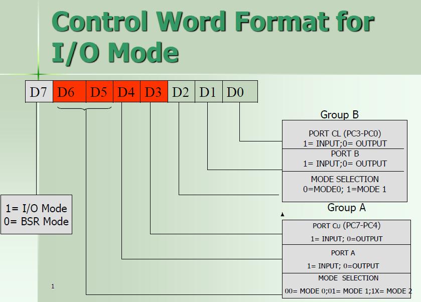
19 Control word and control register 19 CONTROL WORD: control word format for I/O mode is shown in fig below. It is essential to understand this format. In interfacing applications we have to determine the control word for programming the ports for input or output and write it into the CONTROLREGISTER before the data transfer program This way of determining and writing the CONTROL WORD is called I/O programming.
20 20
21 Contd 21 To communicate with periphera1s through 8255A, three steps are necessary Determine the addresses of ports & control register from the chip select logic. Write a control word into the contro1register. Write instructions to transfer data to the peripherals through ports A, B & C
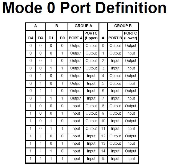
22 22 Mode 0: Simple Input or Output Ports A, B &C are programmed for simple I/O. Data can be simply read from and written to the input and output ports respectively, after appropriate initialization. Outputs are latched. Inputs are -not latched. Ports do not have handshake or interrupt capability. It is used when timing characteristics of I/O devices is well known.
23 Contd. 23.
24 Contd. 24.
25 Contd. 25.
26 Contd. 26.
27 Contd. 27.
28 Contd. 28.
29 Contd. 29.
30 Contd. 30.
31 Contd. 31.
32 32 Example Write instructions to configure 8255 in the following ways. Assume port A address is A0H. All ports as input ports in mode 0. Solution: PA=A0H= PB=A1H= PC=A2H= CR=A3H= Control word BH MVI A, 9BH OUT A3H
33 Exercise 33 Write instructions to configure 8255 in the following ways. Assume port A address is A0H. 1. All ports as output ports in mode PA-O/P, PB-I/P, PCL and PCU-O/P in mode 0 3. Configure Port A as input in Mode 0, Port B as output in mode 0, Port C (Lower) as output and Port C (Upper) as input ports.
34 Contd. 34 Example: -twelve DIP switches are interfaced to 8255 via port B and port CL. Twelve LEDs are interfaced via port A and port C L as shown below. Assume: All ports are in mode 0 i. Identify the port addresses(pa,pb,pc, CW) ii. Determine the control word to configure Ports. i. Write a program to read the DIP switches from port B and port C L and to display the readings at port A and port Cu respectively
35 35
36 36 Contd. Identify the port addresses. Determine the control word to configure port A-& port Cu for output and port B and port C L for input. Write a program to read the DIP switches from port B and port C L and to display the readings at port A and port Cu respectively From the circuit, observe-that the control--signals MEMR and MEMW are connected This indicates to us that the devices-are interfaced in MEMORY MAPPED MODE So, they will have 16-bit addresses. CS is connected to A l5 through an inverter. So A 15 must be at logic high level for the 8255A to be selected.
37 37
38 Contd. 38.
39 Mode 1 Input/output with Handshake 39 In mode 0, which is used for simple I/O, it is assumed that the peripheral devices are always ready The microprocessor, therefore, need not to check their status before transferring data to and from However this is not the case always Sometimes in order to check the-status, the Mp and the peripherals exchange a few signals prior to actual data transfer These signals are called hand shake signals The 8255A's capability to transfer data with handshake is provided in its mode 1 operation
40 Contd 40 Feature of Mode 1: This functional configuration provides a means for transferring I/O data to or from a specified port in conjunction with strobes or handshaking signals. Port A and port B function as 8-bit I/O ports. Each port uses three bits from port C as handshake signals. The remaining two bits from port C can be used for simple I/O. Input-data and output data are latched. used when timing characteristics of I/O devices is not well known, or used when I/O devices supply or receive data at irregular intervals.
41 Mode 1 input Control Signals 41 When port A and port B are configured as input ports, they use three bits each from port C as handshake signals. Port A uses PC3, PC4 and PC5 bits and port B uses PC0, PC1 and PC2 bits. These are shown in figure. These control signals are named STB, IBF and INTR. The purpose, of these signals is as follows.
42 Contd. 42. Fig: Mode 1 Input Configuration
43 Contd. Mode 1 input Control Signals 43 STB (Strobe Input): This is-an active low signal, generated by the input device, when a byte of data is transmitted. On receipt of this signal, the 8255 generates two signals, IBF and INTR. IBF is routed to the input device and INTR to the microprocessor. IBF (Input Buffer Full): This is an active high signal. It tells the peripheral device that the previous byte sent by the device is there in the buffer and the microprocessor is yet to read the same. This kind of acknowledgement and information enables the peripheral to defer sending the next data byte until the buffer is empty, which is indicated by IBF going low. The IBF signal is deactivated when CPU reads the data from input buffer of the respective port by activation of RD signal.
44 Contd. Mode 1 input Control Signals 44 INTR (Interrupt Request): This is an output signal generated by 8255 in response to IBF, STB and INTE (Interrupt enable). This is used to interrupt the microprocessor to read the data byte from the buffer. INTE: It is an internal flip-flop for enabling or disabling INTR signal. The two flip-flops INTEA and INTEB are set/reset by using the BSR mode.
45 Contd. Mode 1 input Control Signals 45 MODE 1 Control word : To configure port A and port B as input ports, the mode 1 control word is as follows.
46 Contd. Mode 1 input Control Signals 46 MODE 1 Status word :The status word is constituted by port C bits. When the microprocessor reads port C, the status word is placed in accumulator. Then the microprocessor can examine the bits to determine the status. The status word is shown below.
47 Mode 1 Output Control Signals 47 When port A and/or port B are configured as output ports, both of them use bits from port C as handshake signals. These handshake signals -are as follows, and are shown in below. Fig : Mode 1 Output Configuration
48 Contd. Mode 1 Output Control Signals 48 OBF: (Output Buffer Full) -This is an active low signal generated by 8255A to indicate to the peripheral that the microprocessor has written one byte of data into the output port and that it is ready to be read by the device from the port. ACK: (Acknowledge): This is an input signal from the peripheral to 8255, indicating that it has received the byte from the port. It is active low.
49 49 Contd. Mode 1 Output Control Signals INTR: (Interrupt Request) - This is an output signal generated by It is set by OBF, ACK and INTE. It can be used to interrupt the MPU for the next data byte. INTE: (Interrupt Enable): This is an internal flip-flop to enable interrupts. The two flip-flows INTEA and INTEB are controlled by the bits PC6 and PC2 respectively through BSR mode. PC4, PC5: These two lines can be setup either as input or output.
50 Contd. Mode 1 Output Control Signals 50 MODE 1 Control word : To configure port A and port B as Output ports, the mode 1 control word is as follows.
51 Contd. Mode 1 Output Control Signals 51 MODE 1 Status word : The status word is accessed by issuing a read to port C. To configure port A and port B as Output ports, the mode 1 control word is as follows.
52 Exercise 52 Write instructions to configure 8255 in the following ways. Assume port A address is A0H. 1. PA-I/P, PB-O/P in mode 1 2. Configure Port A as input in Mode 1, Port B as output in mode 1, Port C7-6 as input ports.
53 Mode 2 Strobed Bidirectional Bus I/O 53 This functional configuration provides a means for communicating with a peripheral device or structure on a single 8-bit bus for both transmitting and receiving data (bidirectional bus I/O). Handshaking signals are provided to maintain proper bus flow discipline in a similar manner to MODE. It is used with an I/O device that receives data some times and sends data sometimes. Ex. Hard disk drive. Mode 2 operation is useful when timing characteristics of I/O devices is not well known, or when I/O devices supply or receive data at irregular intervals.
54 54 Contd. Mode 2 Strobed Bidirectional Bus I/O Port A can be configured as the bidirectional port and Port B either in mode 0 or mode 1. Port A uses five signals from Port C as handshake signals for data transfer. The remaining three lines from Port C can be used either as simple I/O or as handshake signals for Port B. Used in Group A only. One 8-bit, bi-directional bus Port (Port A) and a 5- bit control Port (Port C). Both Inputs and Outputs are latched.
55 Contd. 55.
56 Exercise 56 Write instructions to configure 8255 in the following ways. Assume port A address is A0H. 1. PA-Bidirectional port, PB-I/P in mode 1 2. Configure Port A in Mode 2, Port B as output in mode 1. (PC7-3 are handshake lines for Port A and PC2-0 are handshake signals for port B).
57 Bit Set/Reset, Control word and control 57 register Any of the eight bits of Port C can be Set or Reset using a single Output instruction. In this mode, individual bits of port C can be used for applications such as on On/Off switch. BSR control word has D7 = 0; When Port C is being used as status/control for Port A or B these Bits can be set or reset by using the Bit set/reset operation just as if they were data output port. This feature reduces software requirements in Control-based applications

58 Contd. 58. Fig: BSR Control Word Format in the BSR Mode
59 Exercise 59 Write instructions to configure 8255 in the following ways. Assume port A address is A0H. 1. Set to 1 bit 4 of Port C 0 x x x H Mvi A, 09H out A3H Exercise 1. Reset to 0 bit 6 of Port C
60 Exercise Write instructions to configure 8255 in the following ways. To set PC4 and PC6 pins of port C for 5 mse and reset it after that. Assume : - port A address is B0H. And - delay routine is available. 2. Write a program to blink Port C bit 0 of the 8255 infinitely. Assume address of control word register of 8255 is 83H. Assume: Delay routine is available microprocessor
61 Exercise Consider the interface circuit shown in fig (a) below write a BSR control word subroutine to set PC7 and PC3 and reset them after 10 ms. Assume that delay routine is available.
PIO 8255 (cont..) M Krishna kumar MAM/M3/LU9e/V1/2004 1
 M Krishna kumar MAM/M3/LU9e/V1/2004 1") PIO 8255 (cont..) The parallel input-output port chip 8255 is also called as programmable peripheral input-output port. The Intel s 8255 is designed for use with Intel s 8-bit, 16-bit and higher capability
PIO 8255 (cont..) The parallel input-output port chip 8255 is also called as programmable peripheral input-output port. The Intel s 8255 is designed for use with Intel s 8-bit, 16-bit and higher capability
 Page 1 of 18 Hardware Training Tools Data Acquisition I/O Cards Development Tools Pic Tutor 8255 CHIPS Software CAD Education Consulting Downloads PRICE LIST Corporate About AMS Chronology Contact Sales
8255 Programmable Peripheral Interface Architecture MCT/UNIT III/NARASIMHARAJ/LECTURE NOTES /IV MECH A
 8255 Programmable Peripheral Interface Architecture 8255 PPI Architecture The parallel input-output port chip 8255 is also called as programmable peripheral input- output port. The Intel s 8255 is designed
Lecture-53 Mode 2: (Strobed Bidirectional bus I/O) This functional configuration provides means for communicating with a peripheral device on a
 This functional configuration provides means for communicating with a peripheral device on a") Lecture-53 Mode 2: (Strobed Bidirectional bus I/O) This functional configuration provides means for communicating with a peripheral device on a single 8-bit I/O data bus in both directions, i.e., for both
Lecture-53 Mode 2: (Strobed Bidirectional bus I/O) This functional configuration provides means for communicating with a peripheral device on a single 8-bit I/O data bus in both directions, i.e., for both
82C55. Programmable Peripheral Interface. Interfacing Part III
 82C55 Programmable Peripheral Interface Interfacing Part III Review More on Address decoding Interface with memory Introduction to Programmable Peripheral Interface 82C55 About 82C55 The 82C55 is a popular
Interfacing Fundamentals
 CHAPTER Interfacing Fundamentals 3.1 Introduction There is no doubt that the microcomputer revolution will continue into the future and many will be required to specify and integrate microprocessors into
Week 7. Input/Output Interface Circuits and LSI Peripheral Devices
 Week 7 Input/Output Interface Circuits and LSI Peripheral Devices Core and Special Purpose I/O Interfaces Special purpose I/O interfaces display parallel printer interface serial communication interface
I/O Design. Input / Output Instructions. Engineering 4862 Microprocessors. Lecture 23. Cheng Li
 Engineering 4862 Microprocessors Lecture 23 Cheng Li EN-4012 licheng@engr.mun.ca I/O Design When designing an I/O port, ensure that the port is only active when selected by the microprocessor Use latches
General Purpose Programmable Peripheral Devices. Assistant Professor, EC Dept., Sankalchand Patel College of Engg.,Visnagar
 Chapter 15 General Purpose Programmable Peripheral Devices by Rahul Patel, Assistant Professor, EC Dept., Sankalchand Patel College of Engg.,Visnagar Microprocessor & Interfacing (140701) Rahul Patel 1
Intel 8255 PPI. Presented By: Diwakar Yagyasen Asst. Prof. CSE BBDNITM, Lucknow.
 Intel 8255 PPI Presented By: Diwakar Yagyasen Asst. Prof. CSE BBDNITM, Lucknow. 8255 PPI PPI: Programmable Peripheral Interface 2 Intel 8255 PPI PPI Programmable Peripheral Interface It is an I/O port
Segment A Programmable Peripheral Interface (PPI)
") Segment 6 8255A Programmable Peripheral Interface (PPI) Content Why 8255A? Handshaking and Handshaking Signal Parallel Data Transfer 8255A Internal Block Diagram Description of 8255A Internal Block Diagram
Segment 6 8255A Programmable Peripheral Interface (PPI) Content Why 8255A? Handshaking and Handshaking Signal Parallel Data Transfer 8255A Internal Block Diagram Description of 8255A Internal Block Diagram
9. PERIPHERAL CHIPS 9a
 9. PERIPHERAL CHIPS 9a 8255: Programmable Peripheral Interface. Draw the pin diagram of PPI 8255. Ans. The pin diagram of 8255 is shown in Fig. 9a. PA 3 4 PA 4 PA2 2 39 PA 5 PA 3 38 PA 6 PA 4 37 PA7 RD
Features: 3 8-bit IO ports PA, PB, PC. PA can be set for Modes 0, 1, 2. PB for 0,1 and PC for mode 0 and for BSR. Modes 1 and 2 are interrupt driven.
 Features: 3 8-bit IO ports PA, PB, PC PA can be set for Modes, 1, 2. PB for,1 and PC for mode and for BSR. Modes 1 and 2 are interrupt driven. PC has 2 4-bit parts: PC upper (PCU) and PC lower (PCL), each
EC2304-MICROPROCESSOR AND MICROCONROLLERS 2 marks questions and answers UNIT-I
 EC2304-MICROPROCESSOR AND MICROCONROLLERS 2 marks questions and answers 1. Define microprocessors? UNIT-I A semiconductor device(integrated circuit) manufactured by using the LSI technique. It includes
Basic I/O Interface
 Basic I/O Interface - 8255 11 3 THE PROGRAMMABLE PERIPHERAL 82C55 programmable peripheral interface (PPI) is a popular, low-cost interface component found in many applications. The PPI has 24 pins for
UNIT - II PERIPHERAL INTERFACING WITH 8085
 UNIT - II PERIPHERAL INTERFACING WITH 8085 Peripheral Interfacing is considered to be a main part of Microprocessor, as it is the only way to interact with the external world. The interfacing happens with
INTERFACING INTERFACING. Richa Upadhyay Prabhu. NMIMS s MPSTME February 25, 2016
 INTERFACING Richa Upadhyay Prabhu NMIMS s MPSTME richa.upadhyay@nmims.edu February 25, 2016 8255: Programmable Peripheral Interface or Programmable Input output Device Introduction METHODS OF DATA TRANSFER
Lecture-50 Intel 8255A: Programming and Operating Modes
 Lecture-50 Intel 8255A: Programming and Operating Modes Operation Description: There are three basic modes of operation that can be selected by the system software. Mode 0: Basic Input/output Mode 1: Strobes
UNIT III. 2. Non-maskable interrupts. 3. Software interrupt. 4. Internal interrupt
 UNIT III 8086 INTERRUPTS: An interrupt is the method of processing the microprocessor by peripheral device. An interrupt is used to cause a temporary halt in the execution of program. Microprocessor responds
Lecture Note On Microprocessor and Microcontroller Theory and Applications
 Lecture Note On Microprocessor and Microcontroller Theory and Applications MODULE: 1 1. INTRODUCTION TO MICROPROCESSOR AND MICROCOMPUTER ARCHITECTURE: A microprocessor is a programmable electronics chip
Programmable Peripheral Interface (PPI) 8255A. CEN433 King Saud University Dr. Mohammed Amer Arafah
 8255A. CEN433 King Saud University Dr. Mohammed Amer Arafah") Programmable Peripheral Interface (PPI) 8255A CEN433 King Saud University Dr. 1 Functional Diagram 2 Pin Description 3 8255A Basic Operation A 1 A 0 Port 0 0 Port A 0 1 Port B 1 0 Port C 1 1 Control Word
Programmable Peripheral Interface (PPI) 8255A CEN433 King Saud University Dr. 1 Functional Diagram 2 Pin Description 3 8255A Basic Operation A 1 A 0 Port 0 0 Port A 0 1 Port B 1 0 Port C 1 1 Control Word
Summer 2003 Lecture 21 07/15/03
 Summer 2003 Lecture 21 07/15/03 Simple I/O Devices Simple i/o hardware generally refers to simple input or output ports. These devices generally accept external logic signals as input and allow the CPU
MICROPROCESSOR B.Tech. th ECE
 MICROPROCESSOR B.Tech. th ECE Submitted by: Er. Amita Sharma Dept. of ECE 11/24/2014 2 Microprocessor Architecture The microprocessor can be programmed to perform functions on given data by writing specific
INTRO TO I/O INTERFACE
 Basic I/O Interface Introduction This chapter outlines some of the basic methods of communications, both serial and parallel, between humans or machines and the microprocessor. We first introduce the basic
a8255 Features General Description Programmable Peripheral Interface Adapter
 a8255 Programmable Peripheral Interface Adapter September 1996, ver. 1 Features a8255 MegaCore function implementing a programmable peripheral interface adapter Optimized for FLEX and MAX architectures
Chapter ELEVEN 8255 I/O PROGRAMMING
 Chapter ELEVEN 8255 I/O PROGRAMMING OBJECTIVES this chapter enables the student to: Code Assembly language instructions to read and write data to and from I/O ports. Diagram the design of peripheral I/O
Lab2: 8255 Interfacing
 AL-Hussein Bin Talal University College of Engineering Department of Computer Engineering Computer Interfacing and Peripherals Lab Student Name: Student Number: Dr. Fadi Abu-Amara Eng. Huda Saqallah Lab2:
CHMOS PROGRAMMABLE PERIPHERAL INTERFACE
 CHMOS PROGRMMLE PERIPHERL INTERFCE TECHNICL DT IN2C55 The Integral IN2C55N is a high-performance, CHMOS version of the industry standard IN2C55N general purpose programmable I/O device which is designed
8051 I/O and Class 6 EE4380 Spring 03. Pari vallal Kannan. Center for Integrated Circuits and Systems University of Texas at Dallas
 8051 I/O and 8255 Class 6 EE4380 Spring 03 Pari vallal Kannan Center for Integrated Circuits and Systems University of Texas at Dallas Why I/O Ports Controllers need to get external inputs and produce
1. Internal Architecture of 8085 Microprocessor
 1. Internal Architecture of 8085 Microprocessor Control Unit Generates signals within up to carry out the instruction, which has been decoded. In reality causes certain connections between blocks of the
2. List the five interrupt pins available in INTR, TRAP, RST 7.5, RST 6.5, RST 5.5.
 DHANALAKSHMI COLLEGE OF ENGINEERING DEPARTMENT OF ELECTRICAL AND ELECTRONICS ENGINEERING EE6502- MICROPROCESSORS AND MICROCONTROLLERS UNIT I: 8085 PROCESSOR PART A 1. What is the need for ALE signal in
Topics. Interfacing chips
 8086 Interfacing ICs 2 Topics Interfacing chips Programmable Communication Interface PCI (8251) Programmable Interval Timer (8253) Programmable Peripheral Interfacing - PPI (8255) Programmable DMA controller
1. INTRODUCTION TO MICROPROCESSOR AND MICROCOMPUTER ARCHITECTURE:
 1. INTRODUCTION TO MICROPROCESSOR AND MICROCOMPUTER ARCHITECTURE: A microprocessor is a programmable electronics chip that has computing and decision making capabilities similar to central processing unit
Interrupts. by Rahul Patel, Assistant Professor, EC Dept., Sankalchand Patel College of Engg.,Visnagar
 Chapter 12 Interrupts by Rahul Patel, Assistant Professor, EC Dept., Sankalchand Patel College of Engg.,Visnagar Microprocessor & Interfacing (140701) Rahul Patel 1 Points to be Discussed 8085 Interrupts
These three counters can be programmed for either binary or BCD count.
 S5 KTU 1 PROGRAMMABLE TIMER 8254/8253 The Intel 8253 and 8254 are Programmable Interval Timers (PTIs) designed for microprocessors to perform timing and counting functions using three 16-bit registers.
8086 Interrupts and Interrupt Responses:
 UNIT-III PART -A INTERRUPTS AND PROGRAMMABLE INTERRUPT CONTROLLERS Contents at a glance: 8086 Interrupts and Interrupt Responses Introduction to DOS and BIOS interrupts 8259A Priority Interrupt Controller
MP Assignment III. 1. An 8255A installed in a system has system base address E0D0H.
 MP Assignment III 1. An 8255A installed in a system has system base address E0D0H. i) Calculate the system addresses for the three ports and control register for this 8255A. System base address = E0D0H
MAHALAKSHMI ENGINEERING COLLEGE TIRUCHIRAPALLI UNIT IV I/O INTERFACING PART A (2 Marks)
") MAHALAKSHMI ENGINEERING COLLEGE TIRUCHIRAPALLI-621213. UNIT IV I/O INTERFACING PART A (2 Marks) 1. Name the three modes used by the DMA processor to transfer data? [NOV/DEC 2006] Signal transfer mode (cycling
MAHALAKSHMI ENGINEERING COLLEGE TIRUCHIRAPALLI-621213. UNIT IV I/O INTERFACING PART A (2 Marks) 1. Name the three modes used by the DMA processor to transfer data? [NOV/DEC 2006] Signal transfer mode (cycling
ROEVER ENGINEERING COLLEGE
 ROEVER ENGINEERING COLLEGE ELAMBALUR, PERAMBALUR- 621 212 DEPARTMENT OF INFORMATION TECHNOLOGY MICROPROCESSOR & MICROCONTROLLER 2 marks questions andanswers Unit I 1. Define microprocessor? A microprocessor
8085 Microprocessor Architecture and Memory Interfacing. Microprocessor and Microcontroller Interfacing
 8085 Microprocessor Architecture and Memory 1 Points to be Discussed 8085 Microprocessor 8085 Microprocessor (CPU) Block Diagram Control & Status Signals Interrupt Signals 8085 Microprocessor Signal Flow
UNIT.4. Syllabus I/O INTERFACING 8085
 UNIT.4 I/O INTERFACING 8085 Syllabus Memory Interfacing and I/O interfacing Parallel communication interface Serial communication interface Timer Keyboard /display controller Interrupt controller DMA controller
1. What is Microprocessor? Give the power supply & clock frequency of 8085?
 1. What is Microprocessor? Give the power supply & clock frequency of 8085? A microprocessor is a multipurpose, programmable logic device that reads binary instructions from a storage device called memory
Microprocessors and Microcontrollers (EE-231)
") Microprocessors and Microcontrollers (EE-231) Main Objectives 8088 and 80188 8-bit Memory Interface 8086 t0 80386SX 16-bit Memory Interface I/O Interfacing I/O Address Decoding More on Address Decoding
Microprocessors and Microcontrollers (EE-231) Main Objectives 8088 and 80188 8-bit Memory Interface 8086 t0 80386SX 16-bit Memory Interface I/O Interfacing I/O Address Decoding More on Address Decoding
Overview of Intel 80x86 µp
 CE444 ١ ٢ 8088/808 µp and Supporting Chips Overview of Intel 80x8 µp ٢ ١ 8088/808 µp ٣ Both are mostly the same with small differences. Both are of bit internal Data bus Both have 0 bit address bus Capable
Z Z-280 MT8930, MT8992/3/4/5 MT8880 MT8888 MT8889 MT8980/1 MT8985, MT8986 (DIP-40) MT8986 (PLCC-44) MT8920B MT8952B
 MT8986 (PLCC-44) MT8920B MT8952B") MSAN-145 How to Interface Mitel Components to Parallel Bus CPUs TABL OF CONTNTS Introduction ISSU 1 August 1993 1.0 Group 1 Components 1.1 Interfacing to the 6802 1.2 Interfacing to the 6809 1.3 Interfacing
MSAN-145 How to Interface Mitel Components to Parallel Bus CPUs TABL OF CONTNTS Introduction ISSU 1 August 1993 1.0 Group 1 Components 1.1 Interfacing to the 6802 1.2 Interfacing to the 6809 1.3 Interfacing
MAHARASHTRA STATE BOARD OF TECHNICAL EDUCATION (Autonomous) (ISO/IEC Certified) MODEL ANSWER
 (ISO/IEC Certified) MODEL ANSWER") MODEL ANSWER SUMMER 17 EXAMINATION Subject Title: Microprocessor Subject Code: 17443 I m p o r t a n t I n s t r u c t i o n s t o e x a m i n e r s : 1) The answers should be examined by key words and
MODEL ANSWER SUMMER 17 EXAMINATION Subject Title: Microprocessor Subject Code: 17443 I m p o r t a n t I n s t r u c t i o n s t o e x a m i n e r s : 1) The answers should be examined by key words and
3. The MC6802 MICROPROCESSOR
 3. The MC6802 MICROPROCESSOR This chapter provides hardware detail on the Motorola MC6802 microprocessor to enable the reader to use of this microprocessor. It is important to learn the operation and interfacing
Control Unit: The control unit provides the necessary timing and control Microprocessor resembles a CPU exactly.
 Unit I 8085 and 8086 PROCESSOR Introduction to microprocessor A microprocessor is a clock-driven semiconductor device consisting of electronic logic circuits manufactured by using either a large-scale
C13. INTERFATA PARALELA PROGRAMABILA (PPI) I8255A (PIO)
 I8255A (PIO)") C13. INTERFATA PARALELA PROGRAMABILA (PPI) I8255A (PIO) 1.Descriere PIO 2. Arhitectura PIO 3. Programare PIO 4. PIO in PC 5. Aplicatii http://www.advancedmsinc.com/iocards/8255.htm http://www.eisti.fr/~ga/phy/iitr/ii05/tr.pdf
C13. INTERFATA PARALELA PROGRAMABILA (PPI) I8255A (PIO) 1.Descriere PIO 2. Arhitectura PIO 3. Programare PIO 4. PIO in PC 5. Aplicatii http://www.advancedmsinc.com/iocards/8255.htm http://www.eisti.fr/~ga/phy/iitr/ii05/tr.pdf
S.R.M. INSTITUTE OF SCIENCE & TECHNOLOGY SCHOOL OF ELECTRONICS & COMMUNICATION ENGINEERING
 S.R.M. INSTITUTE OF SCIENCE & TECHNOLOGY SCHOOL OF ELECTRONICS & COMMUNICATION ENGINEERING QUESTION BANK Subject Code : EC307 Subject Name : Microprocessor and Interfacing Year & Sem : III Year, V Sem
History and Basic Processor Architecture
 History and Basic Processor Architecture History of Computers Module 1 Section 1 What Is a Computer? An electronic machine, operating under the control of instructions stored in its own memory, that can
TOPIC 6 LATCH. FIGURE 1 INTERFACING OF ROM/EPROM TO µc 8051.
 TOPIC 6 MEMORY AND I/O INTERFACING MEMORY INTERFACING i. External ROM (program memory) Interfacing P1 P0 D 0-D 7 P3 EA clock LATCH A 0 ROM/ A 7 EPROM A 8 Address lines A 15 PSEN OE FIGURE 1 INTERFACING
Pin Description, Status & Control Signals of 8085 Microprocessor
 Pin Description, Status & Control Signals of 8085 Microprocessor 1 Intel 8085 CPU Block Diagram 2 The 8085 Block Diagram Registers hold temporary data. Instruction register (IR) holds the currently executing
Lecture-51 INTEL 8259A Programmable Interrupt Controller
 Lecture-51 INTEL 8259A Programmable Interrupt Controller The 8259A is a programmable interrupt controller designed to work with Intel microprocessor 8080 A, 8085, 8086, 8088. The 8259 A interrupt controller
INSTITUTE OF ENGINEERING AND MANAGEMENT, KOLKATA Microprocessor
 INSTITUTE OF ENGINEERING AND MANAGEMENT, KOLKATA Microprocessor Subject Name: Microprocessor and Microcontroller Year: 3 rd Year Subject Code: CS502 Semester: 5 th Module Day Assignment 1 Microprocessor
QUESTION BANK. EE 6502 / Microprocessor and Microcontroller. Unit I Processor. PART-A (2-Marks)
") QUESTION BANK EE 6502 / Microprocessor and Microcontroller Unit I- 8085 Processor PART-A (2-Marks) YEAR/SEM : III/V 1. What is meant by Level triggered interrupt? Which are the interrupts in 8085 level
QUESTION BANK EE 6502 / Microprocessor and Microcontroller Unit I- 8085 Processor PART-A (2-Marks) YEAR/SEM : III/V 1. What is meant by Level triggered interrupt? Which are the interrupts in 8085 level
80C451 operation of port 6
 INTRODUCTION The features of the are shared with the 80C5 or are conventional except for the operation of port 6. The flexibility of this port facilitates high-speed parallel data communications. This
Interrupt is a process where an external device can get the attention of the microprocessor. Interrupts can be classified into two types:
 8085 INTERRUPTS 1 INTERRUPTS Interrupt is a process where an external device can get the attention of the microprocessor. The process starts from the I/O device The process is asynchronous. Classification
1 MALP ( ) Unit-1. (1) Draw and explain the internal architecture of 8085.
 Unit-1. (1) Draw and explain the internal architecture of 8085.") (1) Draw and explain the internal architecture of 8085. The architecture of 8085 Microprocessor is shown in figure given below. The internal architecture of 8085 includes following section ALU-Arithmetic
(1) Draw and explain the internal architecture of 8085. The architecture of 8085 Microprocessor is shown in figure given below. The internal architecture of 8085 includes following section ALU-Arithmetic
FIFTH SEMESTER B.TECH DEGREE EXAMINATION MODEL TEST QUESTION PAPER, NOVEMBER CS 305: Microprocessor and Microcontrollers PART A
 Reg No Name FIFTH SEMESTER B.TECH DEGREE EXAMINATION MODEL TEST QUESTION PAPER, NOVEMBER 2017 CS 305: Microprocessor and Microcontrollers Max. Marks: 100 Duration: 3 Hours PART A Answer all questions.
Unit DMA CONTROLLER 8257
 DMA CONTROLLER 8257 In microprocessor based system, data transfer can be controlled by either software or hardware. To transfer data microprocessor has to do the following tasks: Fetch the instruction
Unit-IV Peripheral Interfacing S.Sayeekumar, AP/RMDEEE
 Unit-IV Peripheral Interfacing S.Sayeekumar, AP/RMDEEE 8251 The 8251A is a programmable serial communication interface chip designed for synchronous and asynchronous serial data communication. It supports
4) In response to the the 8259A sets the highest priority ISR, bit and reset the corresponding IRR bit. The 8259A also places
 In response to the the 8259A sets the highest priority ISR, bit and reset the corresponding IRR bit. The 8259A also places") Lecture-52 Interrupt sequence: The powerful features of the 8259A in a system are its programmability and the interrupt routine address capability. It allows direct or indirect jumping to the specific
Lecture-52 Interrupt sequence: The powerful features of the 8259A in a system are its programmability and the interrupt routine address capability. It allows direct or indirect jumping to the specific
Weeks 9-10 Input/Output Interface Circuits and LSI Peripheral Devices Core and Special Purpose I/O Interfaces
 Weeks 9-10 Input/Output Interface Circuits and LSI Peripheral Devices Core and Special Purpose I/O Interfaces Special purpose I/O interfaces are implemented as add-on cards on the PC display parallel printer
8259A - STUDY CARD 1. INTRODUCTION
 8259A - STUDY CARD 1. INTRODUCTION Electro Systems Associates Private Limited (ESA) manufactures trainers for most of the popular microprocessors viz 8085, Z-80, 8031 8086/88, 68000 and 80196. ESA offers
INTEGRATED CIRCUITS. AN408 80C451 operation of port 6
 INTEGRATED CIRCUITS March 1988 INTRODUCTION The features of the are shared with the 80C51 or are conventional except for the operation of port 6. The flexibility of this port facilitates high-speed parallel
Module 3. Embedded Systems I/O. Version 2 EE IIT, Kharagpur 1
 Module 3 Embedded Systems I/O Version 2 EE IIT, Kharagpur 1 Lesson 15 Interrupts Version 2 EE IIT, Kharagpur 2 Instructional Objectives After going through this lesson the student would learn Interrupts
Chapter 4 : Microprocessor System
 Chapter-4 Microprocessor System A microcomputer consists of a set of components or modules of three basic types CPU memory and I/O units which communicate with each other. PIN Configuration of 8085 Fig
Design with Microprocessors
 Design with Microprocessors Year III Computer Science 1-st Semester Lecture 11: I/O transfer with x86 I/O Transfer I/O Instructions We discussed IN, OUT, INS and OUTS as instructions for the transfer of
UNIT-IV. The semiconductor memories are organized as two-dimensional arrays of memory locations.
 UNIT-IV MEMORY INTERFACING WITH 8086: The semi conductor memories are of two types: Static RAM Dynamic RAM The semiconductor memories are organized as two-dimensional arrays of memory locations. For Ex:
Microprocessor Architecture. mywbut.com 1
 Microprocessor Architecture mywbut.com 1 Microprocessor Architecture The microprocessor can be programmed to perform functions on given data by writing specific instructions into its memory. The microprocessor
27 December 2016 Pramod Ghimire. Slide 1 of 16
 8259-Programmable Interrupt Controller (8259-PIC) Slide 1 of 16 Programmable Interface Device A Programmable interface device is designed to perform various input/output functions. Such a device can be
The 8237 DMA Controller: -
 The 8237 DMA Controller: - The 8237 is the LSI controller IC that is widely used to implement the direct memory access (DMA) function in 8088 and 8086 based microcomputer systems. It is available in 40-pin
The functional block diagram of 8085A is shown in fig.4.1.
 Lecture-13 Internal Architecture of Intel 05A The functional block diagram of 05A is shown in fig.4.1. INTA INTR RST7.5 RST5.5 RST6.5 TRAP SOD SID INTERRUPT SERIAL I/O (Internal Bus) FR(S) IR() B() C()
8085 Interrupts. Lecturer, CSE, AUST
 8085 Interrupts CSE 307 - Microprocessors Mohd. Moinul Hoque, 1 Interrupts Interrupt is a process where an external device can get the attention of the microprocessor. The process starts from the I/O device
8/26/2010. Introduction to 8085 BLOCK DIAGRAM OF INTEL Introduction to Introduction to Three Units of 8085
 BLOCK DIAGRAM OF INTEL 8085 GURSHARAN SINGH TATLA Introduction to 8085 It was introduced in 1977. It is 8-bit microprocessor. Its actual name is 8085 A. It is single NMOS device. It contains 6200 transistors
INPUT-OUTPUT ORGANIZATION
 INPUT-OUTPUT ORGANIZATION Peripheral Devices: The Input / output organization of computer depends upon the size of computer and the peripherals connected to it. The I/O Subsystem of the computer, provides
12-Dec-11. Gursharan Singh Maninder Kaur. Introduction to 8085 BLOCK DIAGRAM OF INTEL Introduction to Introduction to 8085
 mailme@gursharansingh.in BLOCK DIAGRAM OF INTEL 8085 mailme@maninderkaur.in Introduction to 8085 It was introduced in 1977. It is 8-bit microprocessor. Its actual name is 8085 A. It is single NMOS device.
Northern India Engineering College, Delhi (GGSIP University) PAPER I
 PAPER I") PAPER I Q1.Explain IVT? ANS. interrupt vector table is a memory space for storing starting addresses of all the interrupt service routine. It stores CS:IP PAIR corresponding to each ISR. An interrupt vector
PAPER I Q1.Explain IVT? ANS. interrupt vector table is a memory space for storing starting addresses of all the interrupt service routine. It stores CS:IP PAIR corresponding to each ISR. An interrupt vector
Chapter NINE 8088,80286 MICROPROCESSORS AND ISA BUS
 Chapter NINE 8088,80286 MICROPROCESSORS AND ISA BUS OBJECTIVES this chapter enables the student to: State the function of the pins of the 8088. List the functions of the 8088 data, address, and control
THE MICROCOMPUTER SYSTEM CHAPTER - 2
 THE MICROCOMPUTER SYSTEM CHAPTER - 2 20 2.1 GENERAL ASPECTS The first computer was developed using vacuum tubes. The computers thus developed were clumsy and dissipating more power. After the invention
PIN DIAGRAM. Richa Upadhyay Prabhu. NMIMS s MPSTME January 19, 2016
 PIN DIAGRAM Richa Upadhyay Prabhu NMIMS s MPSTME richa.upadhyay@nmims.edu January 19, 2016 Richa Upadhyay Prabhu (MPSTME) 8080 Microprocessor January 19, 2016 1 / 51 Pin Diagram of 8086 Richa Upadhyay
MACHINE CONTROL INSTRUCTIONS: 1. EI
 Lecture-33 MACHINE CONTROL INSTRUCTIONS: 1. EI (Enable interrupts): The interrupt system is disabled just after RESET operation. There is an internal INTE F/F (Interrupt enable flipflop) which is reset
Architecture of 8085 microprocessor
 Architecture of 8085 microprocessor 8085 consists of various units and each unit performs its own functions. The various units of a microprocessor are listed below Accumulator Arithmetic and logic Unit
EET2411 DIGITAL ELECTRONICS. A device or electrical circuit used to store a single bit (0 or 1) Ex. FF.
 Ex. FF.") Chapter 12 - Memory Devices Digital information is easily stored Commonly used memory devices and systems will be examined Flip flops Registers VLSI and LSI memory devices The difference between main memory
Chapter 12 - Memory Devices Digital information is easily stored Commonly used memory devices and systems will be examined Flip flops Registers VLSI and LSI memory devices The difference between main memory
Pin diagram Common SignalS Architecture: Sub: 8086 HARDWARE
 1 CHAPTER 6 HARDWARE ARCHITECTURE OF 8086 8086 Architecture: 6.1 8086 Pin diagram 8086 is a 40 pin DIP using CHMOS technology. It has 2 GND s as circuit complexity demands a large amount of current flowing
EC6504-MP&MC, UNIT3 Page 1
 Year/sem: 02/04 UNIT III I/O INTERFACING Academic Year: 2014-2015 (even) 1. What is interfacing? An interface is a shared boundary between the devices which involves sharing information. Interfacing is
Computer Organization (Input-output)
") Computer Organization (Input-output) KR Chowdhary Professor & Head Email: kr.chowdhary@gmail.com webpage: krchowdhary.com Department of Computer Science and Engineering MBM Engineering College, Jodhpur
Computer Organization (Input-output) KR Chowdhary Professor & Head Email: kr.chowdhary@gmail.com webpage: krchowdhary.com Department of Computer Science and Engineering MBM Engineering College, Jodhpur
8051 Microcontroller
 8051 Microcontroller 1 Salient Features (1). 8 bit microcontroller originally developed by Intel in 1980. (2). High-performance CMOS Technology. (3). Contains Total 40 pins. (4). Address bus is of 16 bit
Basics of Microprocessor
 Unit 1 Basics of Microprocessor 1. Microprocessor Microprocessor is a multipurpose programmable integrated device that has computing and decision making capability. This semiconductor IC is manufactured
1. Internal Architecture of 8085 Microprocessor
 Practical 1 Date : AIM : Introduction Of Microprocessor 8085. 1. Internal Architecture of 8085 Microprocessor Control Unit Generates signals within µp to carry out the instruction, which has been decoded.
MICROPROCESSOR MICROPROCESSOR. From the above description, we can draw the following block diagram to represent a microprocessor based system: Output
 8085 SATISH CHANDRA What is a Microprocessor? The word comes from the combination micro and processor. Processor means a device that processes whatever. In this context, processor means a device that processes
Chapter 8 Summary: The 8086 Microprocessor and its Memory and Input/Output Interface
 Chapter 8 Summary: The 8086 Microprocessor and its Memory and Input/Output Interface Figure 1-5 Intel Corporation s 8086 Microprocessor. The 8086, announced in 1978, was the first 16-bit microprocessor
Microprocessor Architecture
 Microprocessor - 8085 Architecture 8085 is pronounced as "eighty-eighty-five" microprocessor. It is an 8-bit microprocessor designed by Intel in 1977 using NMOS technology. It has the following configuration
The 8255A: Programmable Peripheral Interface
 CMP:885 Peripherals Summary- EE39: Computer Organization, rchitecture and MicroProcessors http://www.ee.iitb.ac.in/ sumantra/courses/up/up.html The 855: Programmable Peripheral Interface PROGRMMER S VIEW
The Purpose of Interrupt
 Interrupts 3 Introduction In this chapter, the coverage of basic I/O and programmable peripheral interfaces is expanded by examining a technique called interrupt-processed I/O. An interrupt is a hardware-initiated
Address connections Data connections Selection connections
 Interface (cont..) We have four common types of memory: Read only memory ( ROM ) Flash memory ( EEPROM ) Static Random access memory ( SARAM ) Dynamic Random access memory ( DRAM ). Pin connections common
Chapter 13 Direct Memory Access and DMA-Controlled I/O
 Chapter 13 Direct Memory Access and DMA-Controlled I/O The DMA I/O technique provides direct access to the memory while the microprocessor is temporarily disabled This allows data to be transferred between
PART - B (Answer all five units, 5 X 10 = 50 Marks)
") Code: 13A04507 R13 B.Tech III Year I Semester (R13) Supplementary Examinations June 2017 MICROPROCESSS & INTERFACING (Common to CSE & IT) PART - A (a) Mention the function of the instruction ADD M of 8085
Code: 13A04507 R13 B.Tech III Year I Semester (R13) Supplementary Examinations June 2017 MICROPROCESSS & INTERFACING (Common to CSE & IT) PART - A (a) Mention the function of the instruction ADD M of 8085
The advantages of registers over memory locations are as follows:
 Q.2 a. In a microprocessor, what is the use of a register? What are the advantages & disadvantages of using registers over a memory location? What is the speciality of register A (accumulator) over other