FPGA Based Digital Signal Processing Applications & Techniques. Nathan Eddy Fermilab BIW12 Tutorial
|
|
|
- Eunice Higgins
- 6 years ago
- Views:
Transcription
1 FPGA Based Digital Signal Processing Applications & Techniques BIW12 Tutorial
2 Outline Digital Signal Processing Basics Modern FPGA Overview Instrumentation Examples
3 Advantages of Digital Signal Processing (DSP) NO DRIFT due to temperature or age ACCURACY defined by number of bits PREDICTABILITY from simulation PERFORMANCE Linear Phase Response possible Adaptability in terms of resources PRODUCTION identical units, no tuning FLEXIBILITY via firmware modifications DYNAMIC RANGE
4 For Beam Instrumentation Need to work with analog input signals Beam pickups, Schottky detectors, Torroids, etc Requires Analog to Digital Converters (ADCs) Need to produce analog output signals To act on the beam RF, kick signals, etc Require Digital to Analog Converters (DACs) The effectiveness of FPGA solutions is largely dominated by the performance of the converters
5 Practical Limitations of Sampling Common sources of sampling error Aliasing Quantization Sample Clock Jitter Can be characterized by their impact on the Signal to Noise Ratio (SNR) of the sampled signal SNR ~ log(sa/na) Typically expressed in decibels (db)
 where (t) = The sequence Si")
 The sampling frequency Fs")
6 Discrete Time Sampling Si = S(t)* (t) where (t) = The sequence Si is the sampled version of S(t) (t-nt) The sampling frequency Fs is 1/T

7 Sampling Theorem For ideal reconstruction Fs > 2B where B is the highest frequency in the signal of interest Sampling ambiguity
8 Aliasing Signals at frequencies larger Fs/2 than will alias into the first Nyquist band Undersampling makes use of this effect
9 Quantization Results in signal noise SNRdb = N, N=number of bits
10 Oversampling Improves SNR Gain SNRdb = 10log(R) where R=Fs/2B Fs is the sampling Frequency B is signal bandwidth Also relaxes the requirements on the antialiasing analog filter
11 Sampling Clock Jitter Another source of signal noise Proportional to maximum signal frequency, fmax RMS sampling clock jitter, Ta SNRdb = 20log(1/(2 fmaxta)) A significant effect for undersampling applications
12 Theoretical SNR Comparison
13 The Z domain A sampled sequence, x(n) can be represented X(z) = n=0 x(n)z-n Where z-1 is the unit delay related to the sample period (T) X(z) is the z-transform of x(n)
14 Difference Eq & Transfer Function A constant coefficient difference equation is a recursive relationship where-by the output of a discrete time system can be calculated using a combination of past output values and past and present input values N k=0 aky[n-k] = M k=0 Gives z-domain transfer function, H(z) H(z) = Y(z) = X(z) bkx[n-k] M -k b z k k=0 N -k a z k k=0 Digital filters are specified by a,b coefficients
15 Infinite Impulse Response (IIR) Filter Feedback provides infinite impulse response an non-zero for n 1 Properties Very efficient Non-linear Phase Can be unstable Feedforward Feedback
16 Finite Impulse Response (FIR) Filter Nth Order FIR filter Just the feedforward block a0=1, all others zero Has linear phase if coefficients are symmetric That is {b0,,bn} = {bn,,b0} No analog equivalent
17 Cascade Integrating Comb (CIC) Filter Comb Filter Integrator H(z) = 1-z-RM H(z) = 1/(1+z-1) For an Nth Order CIC Filter, the transfer function is (1-z-RM)N RM-1 -k N H(z) = =( z ) -1 N (1+z ) k=0 Equivalent to N FIR filters with unit coefficients -> symmetric Linear Phase even though it has infinite response filter sections Used as very efficient way to filter and change rate Can be used as Interpolation filter by reversing I & C sections
18 Quadrature Signals, I & Q Complex signal representation Imag Q(t) A(t) φ(t) Real I(t) In-Phase (real) & Quadrature (imaginary) I(t) = A(t)cos(φ(t)) Q(t) = A(t)sin(φ(t))
19 Digital Down-Conversion cos(2 f) X I = Xcos(2 f) Signal X sin(2 f) X Multiply a signal X by sin(2 f) & cos(2 f) where f is the the down-conversion frequency Q = Xsin(2 f) Shifts the spectral components of X down in frequency by f Commonly followed by decimating low pass filter Remove sum frequency components Process narrow bandwidth signals at lower rate in baseband
20 Discrete Fourier Transform (DFT) Discrete Fourier Transform of length N X(k) = N-1 n=0 x(n) [cos(2 nk/n) +isin(2 nk/n)] X(k) determines the complex signal contribution of the frequency in the composition of x(n) Phase or direction (forward, inverse) given by the sign of the imaginary term
21 Fast Fourier Transform (FFT) Works as a bank of band-pass filters An N point DFT requires N2 operations Can compute the N point DFT as two N/2 point DFTs The output magnitude from each filter is proportional to the input energy in each band Extrapolate to the limit where N is a power of 2 for an N point FFT An N point FFT requires N/2log2(N) operations Note, FFT are almost always implemented as a power of 2 but can be any prime factor
22 Outline Digital Signal Processing Basics Modern FPGA Overview Instrumentation Examples
23 FPGA Advantages for DSP Parallel processing power (Speed) Pipeline architecture Able to consume large quantities of data Alleviate bandwidth bottlenecks in front-ends Efficient digital filter implementation Perform operations under strict timing (latency) control Dedicated DSP (multiplier) blocks Flexibility Clocking synchronous with accelerator Easy integration with ADCs and DACs Easy to modify algorithms and functionality

24 High End FPGA Architecture
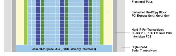
25 Flexible I/O Options Dedicated hardware support for almost all standard I/O protocols Transceivers with equalization for fast differential serial I/O External memory interface support PCI Express, RapidIO, etc Support for over 20GBps links! DDR, DDR2, DDR3 Speed and quantity of available I/O -> $$


26 Clock Domains and Distribution Networks Multiple PLLs and DLLs for sophisticated clock management Support for run-time reconfiguration Fractional PLLs for arbitrary clock synthesis Dedicated global and regional clock distribution networks Support high rate synchronous design Support parallel & pipelined design Up to 16 Global Clocks Up to 23 Regional Clocks per Quadrant
27 Synchronous Design - Pipelining Reliable designs require synchronous design principles Increase speed and bandwidth Trade resources and latency Simple Delay Pipeline Data Clock


28 Digital Signal Processing (DSP) Blocks Based upon dedicated multiplier blocks Provide efficient flexibility and power Fully customize, dedicated support for FIRs, FFT, etc to optimize for speed and efficiency Modern blocks provide capability for 32 or 64 bit floating point operations
29 Integer Representation 2s Complement N Bit representation N-1 Sign Bit (N-1) Integer Bits 2N Positive numbers just simple binary representation Negative numbers are binary number that when added to a positive number of the same magnitude equals zero Convenient Properties Simple arithmetic addition & subtraction the same 2N = IBs all 1-2N-1-2N = IBs all 0
30 Fixed Point Signal Processing Bit widths double on each multiply! Need to control bit widths for efficient resource use Truncation or Rounding Saturation or Roll-over Fixed Point N Bit Representation N-1 M 0 Sign Integer Bits Fractional Bits Bit M Can facilitate keeping track of bit widths
31 Floating Point Representation IEEE-754 Standard Followed Sign Exponent Bit 32 bit Single Precision 8 bit Exponent & 23 bit Mantissa 64 bit Double Precision Mantissa 11 bit Exponent & 52 bit Mantissa Single-Extended Precision Exponent and Mantissa widths are not fixed Minimum 11 Exponent Bits (Exponent<Mantissa) Minimum 31Mantissa Bits Total Bits at least 43 up to 64
32 Running Average Example Can implement an N sample running average as an FIR with N taps with coefficients of 1/N Can be efficiently implemented using two accumulators and a delay line x[n] z-n Acc Acc - /N y[n]
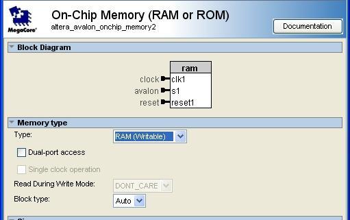
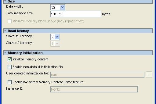
33 Intellectual Property (IP) Cores Functional cores which can be used to greatly speed up and simplify the design process Each FPGA manufacturer provides cores for all basic components PLLs, RAM, FIFOs, Flip-Flops, etc Accumulators, Add, Sub, Multiply, Divide, etc Take advantage of chip resources Advanced cores available for almost any task Simple implementation via GUI parametrization


34 Embedded Systems Hard Core Embedded processor is a dedicated physical component of the chip, separate from the programmable logic 2-4 times faster than Soft Core More efficient if you need a processor Soft Core Embedded processor is built out of the programmable logic on the chip Hard Core Resource Allocation A 32 bit RISC processor uses about few percent of total resources Have option to re-allocate resources if processor not needed Soft Core Resource Allocation
35 System On a Programmable Chip (SOPC) A wide variety of design tools and options available Focus upon developing System On a Programmable Chip Pure HDL entry still possible Aim to simplify the design process as chip architectures become more complicated Tightly couple design and simulation at all levels
36 Outline Digital Signal Processing Basics Modern FPGA Overview Instrumentation Examples

37 Booster Digital Damper


38 Digital Damper Board 4 DACs DDR SoDIMM Big FPGA 4 ADCs

39 Firmware Overview 84 FIRs In parallel Beam Pos Beam Kick Design operates synchronous with Booster RF sweeping from 37MHz to 53MHz Provides bucket by bucket damping on all 84 Booster bunches
40 ADC Input clocked at 4*RF RF Ref PLL 4RF ADC 4RF LVDS RX RF RF FIFO ADC clock is shifted to provide ideal sampling FIFO used to shift data from ADC clock to internal clock
41 RF Reference PLL Use one of the Enhanced PLLs Real-time reconfigurability Dedicated clock pin for RF Reference Directly connected to clock output pins for each ADC clock Use to adjust phase of ADC clock in 15º increments 50Mhz) Instantiated with parametrized IP
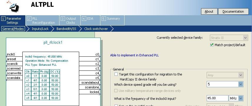
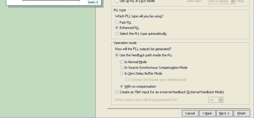
42 PLL Instantiation
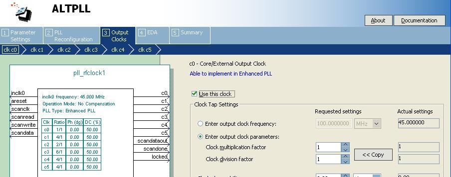
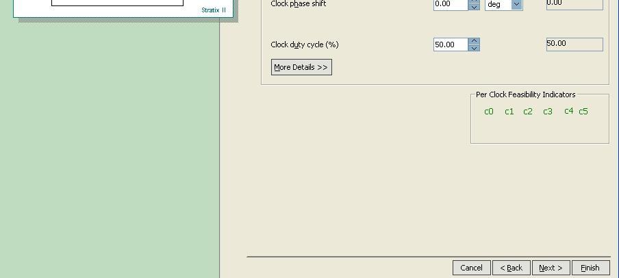
43 PLL Instantiation
44 LVDS Receiver Instantiated with parametrized IP Able to take full advantage of built in RX blocks Dynamic Phase Alignment circuitry Automatically de-serialize data from 4*RF rate to 4 time multi-plexed samples at RF rate No need to worry about timing constraints!

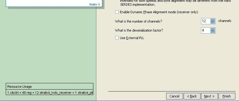
45 LVDS Receiver IP

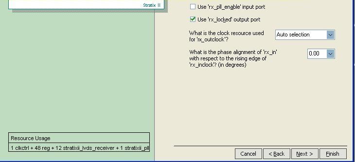
46 LVDS Receiver IP

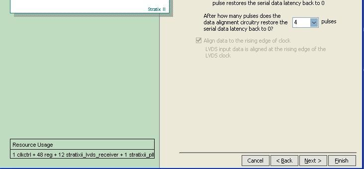
47 LVDS Receiver IP
48 Programmable Delay Dual-port RAM to provide programmable delay Offset read & write pointer to requested delay value Reset Read Counter to zero when Write Counter = Delay-1 Maximum delay set by the depth of the RAM Data Clock Write Counter Read Counter Clock WrAddr RdAddr RdData WrData Data In Dual-port RAM Data Out
49 Handling Frequency Sweep Digital Portion of design is operating locked to the Booster RF and sweeps along with it Need to adjust output delay to account for fixed input/output cable & amplifier delays Use lookup table to specify output delay Clock Turn Counter Look-up Table RAM Delay Out Turn Marker Enable
50 Implementation of Fine Delay Filter produces kick for each RF bucket Operate DAC at 12*RF clock rate Latch 12 LVDS TX To DAC Can shift data fed to LVDS Transmitter to provide RF/12 delay resolution
 within the machine cycle Select bunch position to pass to FFT engine Measure response of single bunch over 128")
51 Tune Measurement 128 Turn Excite single bunch with noise via the damper Simple State Machine to Control Measurement User programmable excitation, noise or anti-damping Can vary gain and duration of excitation at each measurement point Up to 64 measurements at selectable time (turn) within the machine cycle Select bunch position to pass to FFT engine Measure response of single bunch over 128 turns Instantiate fixed point FFT using commercial IP
52 Tune Measurement

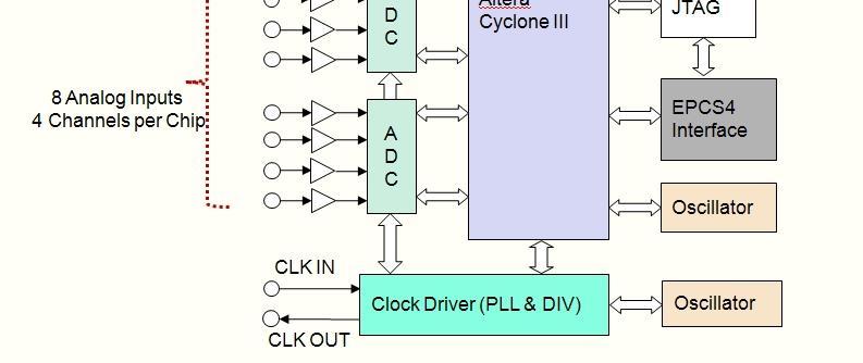
53 8 Channel 125MS/s Digitizer


54 Digital BPM Receiver Firmware
 CIC filters operating in parallel at 71MHz Serial FIR filter at 4.")
55 Narrowband (Closed Orbit) Filter Beam Calib Digital Down Converter (DDC) Section 32 separate filter paths simultaneously 8 channels, I&Q, 2 frequencies (beam, calibration) CIC filters operating in parallel at 71MHz Serial FIR filter at 4.2KHz

56 Numerically Controlled Oscillator (NCO) IP Generate Sin & Cos signals at requested frequency Frequency Output = FCLKPhi/2N Frequency Resolution = FCLK/2N
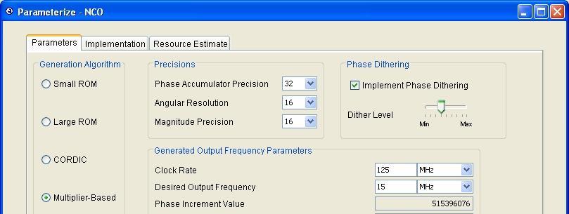
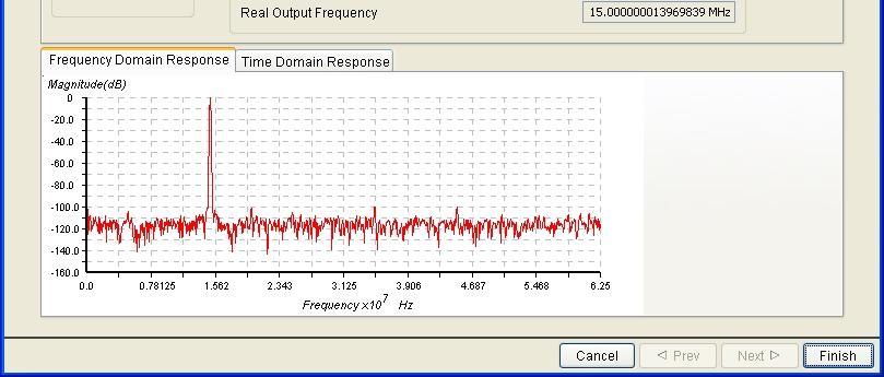
57 NCO IP


58 DDC Quantization Error Will always have a slight offset between the NCO frequency and the beam frequency Easy solution is to offset the NCO frequency to get an integer number of periods in the averaging window


59 CIC Filter IP Commercial IP allows for single instantiation for all 32 CIC filters needed Provides standard serial data output which can be directly interfaced to serial FIR filter


60 FIR Filter IP Provides simple filter design tool or ability to import filter coefficients Option to allow modification of coefficients
61 System Integration Tools Streamline system integration and design Use well defined interfaces Connect standard interfaces Internal memory, external memory, configuration devices, etc Connect custom interfaces Easy CPU integration Handles addressing & interrupts Even generates drivers for system components! Generates all logic for system interconnects! Handles all the timing - clock domains, multiplexing, etc Built in error checking at compile time Facilitates implementing re-usable HDL blocks and group design methodologies


62 System Integration Tool Example System Clocks Design Comps Component Library

63 System Integration Tool Example
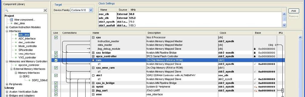
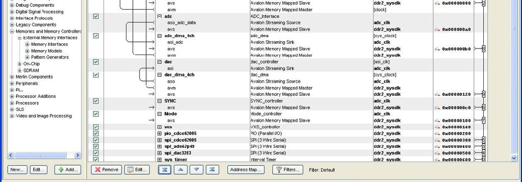
64 System Integration Tool Example
65 Summary - the FPGA Pitch Sure things Looks promising FPGA are now the acknowledged leader of cutting edge fast DSP applications where speed and flexibility are needed Accelerator Control and Instrumentation is already using FPGAs to implement fast online applications, especially feedback & control The size, speed, and feature sets continue to grow by leaps and bounds Today s mid level chips are offering features only available in high end chips just a few years ago at a fraction of the cost Design tools are getting closer to traditional programming and becoming easier to use Use of FPGA s to implement online orbit measurements and optic calcuations which could be used for realtime feedback The next step is cluster and mesh architectures using FPGAs to further increase the processing power It could happen.. FPGA based co-processors for dedicated calculations FPGA based super computers which configure their hardware to optimize the performance for the algorithms being used

66 Thanks for Your Attention!
REAL TIME DIGITAL SIGNAL PROCESSING
 REAL TIME DIGITAL SIGNAL PROCESSING UTN - FRBA 2011 www.electron.frba.utn.edu.ar/dplab Introduction Why Digital? A brief comparison with analog. Advantages Flexibility. Easily modifiable and upgradeable.
Fatima Michael College of Engineering & Technology
 DEPARTMENT OF ECE V SEMESTER ECE QUESTION BANK EC6502 PRINCIPLES OF DIGITAL SIGNAL PROCESSING UNIT I DISCRETE FOURIER TRANSFORM PART A 1. Obtain the circular convolution of the following sequences x(n)
Parallel FIR Filters. Chapter 5
 Chapter 5 Parallel FIR Filters This chapter describes the implementation of high-performance, parallel, full-precision FIR filters using the DSP48 slice in a Virtex-4 device. ecause the Virtex-4 architecture
REAL TIME DIGITAL SIGNAL PROCESSING
 REAL TIME DIGITAL SIGNAL PROCESSING UTN-FRBA 2010 Introduction Why Digital? A brief comparison with analog. Advantages Flexibility. Easily modifiable and upgradeable. Reproducibility. Don t depend on components
19. Implementing High-Performance DSP Functions in Stratix & Stratix GX Devices
 19. Implementing High-Performance SP Functions in Stratix & Stratix GX evices S52007-1.1 Introduction igital signal processing (SP) is a rapidly advancing field. With products increasing in complexity,
LWA DRX C Language Simulation Report - v0.1
 LWA DRX C Language Simulation Report - v0.1 Johnathan York (ARL:UT) February 1, 2008 1 Introduction This document contains a short report on the Long Wavelength Array (LWA) Digital Receiver (DRX) C simulator
How to validate your FPGA design using realworld
 How to validate your FPGA design using realworld stimuli Daniel Clapham National Instruments ni.com Agenda Typical FPGA Design NIs approach to FPGA Brief intro into platform based approach RIO architecture
CHAPTER 4. DIGITAL DOWNCONVERTER FOR WiMAX SYSTEM
 CHAPTER 4 IMPLEMENTATION OF DIGITAL UPCONVERTER AND DIGITAL DOWNCONVERTER FOR WiMAX SYSTEM 4.1 Introduction FPGAs provide an ideal implementation platform for developing broadband wireless systems such
D. Richard Brown III Professor Worcester Polytechnic Institute Electrical and Computer Engineering Department
 D. Richard Brown III Professor Worcester Polytechnic Institute Electrical and Computer Engineering Department drb@ece.wpi.edu Lecture 2 Some Challenges of Real-Time DSP Analog to digital conversion Are
D. Richard Brown III Associate Professor Worcester Polytechnic Institute Electrical and Computer Engineering Department
 D. Richard Brown III Associate Professor Worcester Polytechnic Institute Electrical and Computer Engineering Department drb@ece.wpi.edu 3-November-2008 Analog To Digital Conversion analog signal ADC digital
Implementation of a Low Power Decimation Filter Using 1/3-Band IIR Filter
 Implementation of a Low Power Decimation Filter Using /3-Band IIR Filter Khalid H. Abed Department of Electrical Engineering Wright State University Dayton Ohio, 45435 Abstract-This paper presents a unique
Method We follow- How to Get Entry Pass in SEMICODUCTOR Industries for 3rd year engineering. Winter/Summer Training
 Method We follow- How to Get Entry Pass in SEMICODUCTOR Industries for 3rd year engineering Winter/Summer Training Level 2 continues. 3 rd Year 4 th Year FIG-3 Level 1 (Basic & Mandatory) & Level 1.1 and
Digital Filters in Radiation Detection and Spectroscopy
 Digital Filters in Radiation Detection and Spectroscopy Digital Radiation Measurement and Spectroscopy NE/RHP 537 1 Classical and Digital Spectrometers Classical Spectrometer Detector Preamplifier Analog
REAL TIME DIGITAL SIGNAL PROCESSING
 REAL TIME DIGITAL SIGNAL PROCESSING SASE 2010 Universidad Tecnológica Nacional - FRBA Introduction Why Digital? A brief comparison with analog. Advantages Flexibility. Easily modifiable and upgradeable.
Selecting PLLs for ASIC Applications Requires Tradeoffs
 Selecting PLLs for ASIC Applications Requires Tradeoffs John G. Maneatis, Ph.., President, True Circuits, Inc. Los Altos, California October 7, 2004 Phase-Locked Loops (PLLs) are commonly used to perform
VIII. DSP Processors. Digital Signal Processing 8 December 24, 2009
 Digital Signal Processing 8 December 24, 2009 VIII. DSP Processors 2007 Syllabus: Introduction to programmable DSPs: Multiplier and Multiplier-Accumulator (MAC), Modified bus structures and memory access
isplever Parallel FIR Filter User s Guide October 2005 ipug06_02.0
 isplever TM CORE Parallel FIR Filter User s Guide October 2005 ipug06_02.0 Introduction This document serves as a guide containing technical information about the Lattice Parallel FIR Filter core. Overview
Representation of Numbers and Arithmetic in Signal Processors
 Representation of Numbers and Arithmetic in Signal Processors 1. General facts Without having any information regarding the used consensus for representing binary numbers in a computer, no exact value
EQUALIZER DESIGN FOR SHAPING THE FREQUENCY CHARACTERISTICS OF DIGITAL VOICE SIGNALS IN IP TELEPHONY. Manpreet Kaur Gakhal
 EQUALIZER DESIGN FOR SHAPING THE FREQUENCY CHARACTERISTICS OF DIGITAL VOICE SIGNALS IN IP TELEPHONY By: Manpreet Kaur Gakhal A THESIS SUBMITTED IN PARTIAL FULFILLMENT OF THE REQUIREMENTS FOR THE DEGREE
ECE4703 B Term Laboratory Assignment 2 Floating Point Filters Using the TMS320C6713 DSK Project Code and Report Due at 3 pm 9-Nov-2017
 ECE4703 B Term 2017 -- Laboratory Assignment 2 Floating Point Filters Using the TMS320C6713 DSK Project Code and Report Due at 3 pm 9-Nov-2017 The goals of this laboratory assignment are: to familiarize
Filterbanks and transforms
 Filterbanks and transforms Sources: Zölzer, Digital audio signal processing, Wiley & Sons. Saramäki, Multirate signal processing, TUT course. Filterbanks! Introduction! Critical sampling, half-band filter!
PCI-16HSDI: 16-Bit, Six-Channel Sigma-Delta Analog Input PMC Board. With 1.1 MSPS Sample Rate per Channel, and Two Independent Clocks
 PMC-16HSDI 16-Bit, Six-Channel Sigma-Delta Analog Input PMC Board With 1.1 MSPS Sample Rate per Channel, and Two Independent Clocks Available also in PCI, cpci and PC104-Plus form factors as: PCI-16HSDI:
Introduction to Field Programmable Gate Arrays
 Introduction to Field Programmable Gate Arrays Lecture 2/3 CERN Accelerator School on Digital Signal Processing Sigtuna, Sweden, 31 May 9 June 2007 Javier Serrano, CERN AB-CO-HT Outline Digital Signal
Virtex-II Architecture. Virtex II technical, Design Solutions. Active Interconnect Technology (continued)
") Virtex-II Architecture SONET / SDH Virtex II technical, Design Solutions PCI-X PCI DCM Distri RAM 18Kb BRAM Multiplier LVDS FIFO Shift Registers BLVDS SDRAM QDR SRAM Backplane Rev 4 March 4th. 2002 J-L
Virtex-II Architecture SONET / SDH Virtex II technical, Design Solutions PCI-X PCI DCM Distri RAM 18Kb BRAM Multiplier LVDS FIFO Shift Registers BLVDS SDRAM QDR SRAM Backplane Rev 4 March 4th. 2002 J-L
Chapter 1 Introduction
 Chapter 1 Introduction The Motorola DSP56300 family of digital signal processors uses a programmable, 24-bit, fixed-point core. This core is a high-performance, single-clock-cycle-per-instruction engine
Head, Dept of Electronics & Communication National Institute of Technology Karnataka, Surathkal, India
 Mapping Signal Processing Algorithms to Architecture Sumam David S Head, Dept of Electronics & Communication National Institute of Technology Karnataka, Surathkal, India sumam@ieee.org Objectives At the
Xilinx DSP. High Performance Signal Processing. January 1998
 DSP High Performance Signal Processing January 1998 New High Performance DSP Alternative New advantages in FPGA technology and tools: DSP offers a new alternative to ASICs, fixed function DSP devices,
Data Manual GC4016 MULTI-STANDARD QUAD DDC CHIP
 Data Manual PRODUCTION DATA information is current as of publication date. Products conform to specifications per the terms of the Texas Instruments standard warranty. Production processing does not necessarily
New Software-Designed Instruments
 1 New Software-Designed Instruments Nicholas Haripersad Field Applications Engineer National Instruments South Africa Agenda What Is a Software-Designed Instrument? Why Software-Designed Instrumentation?
Image Compression System on an FPGA
 Image Compression System on an FPGA Group 1 Megan Fuller, Ezzeldin Hamed 6.375 Contents 1 Objective 2 2 Background 2 2.1 The DFT........................................ 3 2.2 The DCT........................................
GC2011A 3.3V DIGITAL FILTER CHIP DATASHEET. March 21, 2000
 GC2011A 3.3V DIGITAL FILTER CHIP DATASHEET March 21, 2000 Information provided by Graychip is believed to be accurate and reliable. No responsibility is assumed by Graychip for its use, nor for any infringement
Basic Xilinx Design Capture. Objectives. After completing this module, you will be able to:
 Basic Xilinx Design Capture This material exempt per Department of Commerce license exception TSU Objectives After completing this module, you will be able to: List various blocksets available in System
ECE 450:DIGITAL SIGNAL. Lecture 10: DSP Arithmetic
 ECE 450:DIGITAL SIGNAL PROCESSORS AND APPLICATIONS Lecture 10: DSP Arithmetic Last Session Floating Point Arithmetic Addition Block Floating Point format Dynamic Range and Precision 2 Today s Session Guard
Digital Signal Processing with Field Programmable Gate Arrays
 Uwe Meyer-Baese Digital Signal Processing with Field Programmable Gate Arrays Third Edition With 359 Figures and 98 Tables Book with CD-ROM ei Springer Contents Preface Preface to Second Edition Preface
Computational Methods. H.J. Bulten, Spring
 Computational Methods H.J. Bulten, Spring 2017 www.nikhef.nl/~henkjan 1 Lecture 1 H.J. Bulten henkjan@nikhef.nl website: www.nikhef.nl/~henkjan, click on Computational Methods Aim course: practical understanding
Field Programmable Gate Array (FPGA)
") Field Programmable Gate Array (FPGA) Lecturer: Krébesz, Tamas 1 FPGA in general Reprogrammable Si chip Invented in 1985 by Ross Freeman (Xilinx inc.) Combines the advantages of ASIC and uc-based systems
Field Programmable Gate Array (FPGA) Lecturer: Krébesz, Tamas 1 FPGA in general Reprogrammable Si chip Invented in 1985 by Ross Freeman (Xilinx inc.) Combines the advantages of ASIC and uc-based systems
Classification of Semiconductor LSI
 Classification of Semiconductor LSI 1. Logic LSI: ASIC: Application Specific LSI (you have to develop. HIGH COST!) For only mass production. ASSP: Application Specific Standard Product (you can buy. Low
RISC IMPLEMENTATION OF OPTIMAL PROGRAMMABLE DIGITAL IIR FILTER
 RISC IMPLEMENTATION OF OPTIMAL PROGRAMMABLE DIGITAL IIR FILTER Miss. Sushma kumari IES COLLEGE OF ENGINEERING, BHOPAL MADHYA PRADESH Mr. Ashish Raghuwanshi(Assist. Prof.) IES COLLEGE OF ENGINEERING, BHOPAL
Chapter 2. Cyclone II Architecture
 Chapter 2. Cyclone II Architecture CII51002-1.0 Functional Description Cyclone II devices contain a two-dimensional row- and column-based architecture to implement custom logic. Column and row interconnects
HIGH SPEED SIGNAL CHAIN SELECTION GUIDE
 HIGH SPEED SIGNAL CHAIN SELECTION GUIDE Includes High Speed Cs, DACs, Amplifiers, and Clocking Solutions Visit analog.com and linear.com High Speed Signal Chain Product Selection Guide TABLE OF CONTENTS
4.1 QUANTIZATION NOISE
 DIGITAL SIGNAL PROCESSING UNIT IV FINITE WORD LENGTH EFFECTS Contents : 4.1 Quantization Noise 4.2 Fixed Point and Floating Point Number Representation 4.3 Truncation and Rounding 4.4 Quantization Noise
DIGITAL SYSTEM. Technology Overview Nordco. All rights reserved. Rev C
 DIGITAL SYSTEM Technology Overview Rev C 01-05-2016 Insert Full Frame Product Picture Here 2015 KEY FEATURES DIGITAL PROCESSING SYSTEM FOR INDUSTRIAL & TONNE UE SYSTEM DIGITAL PROCESSING SYSTEM FOR MICRO
Chapter 03: Computer Arithmetic. Lesson 09: Arithmetic using floating point numbers
 Chapter 03: Computer Arithmetic Lesson 09: Arithmetic using floating point numbers Objective To understand arithmetic operations in case of floating point numbers 2 Multiplication of Floating Point Numbers
Intel Stratix 10 Clocking and PLL User Guide
 Intel Stratix 10 Clocking and PLL User Guide Updated for Intel Quartus Prime Design Suite: 18.0 Subscribe Send Feedback Latest document on the web: PDF HTML Contents Contents 1. Intel Stratix 10 Clocking
Qsys and IP Core Integration
 Qsys and IP Core Integration Stephen A. Edwards (after David Lariviere) Columbia University Spring 2016 IP Cores Altera s IP Core Integration Tools Connecting IP Cores IP Cores Cyclone V SoC: A Mix of
Evaluating MMX Technology Using DSP and Multimedia Applications
 Evaluating MMX Technology Using DSP and Multimedia Applications Ravi Bhargava * Lizy K. John * Brian L. Evans Ramesh Radhakrishnan * November 22, 1999 The University of Texas at Austin Department of Electrical
REAL-TIME DIGITAL SIGNAL PROCESSING
 REAL-TIME DIGITAL SIGNAL PROCESSING FUNDAMENTALS, IMPLEMENTATIONS AND APPLICATIONS Third Edition Sen M. Kuo Northern Illinois University, USA Bob H. Lee Ittiam Systems, Inc., USA Wenshun Tian Sonus Networks,
Digital Signal Processing Lecture Notes 22 November 2010
 Digital Signal Processing Lecture otes 22 ovember 2 Topics: Discrete Cosine Transform FFT Linear and Circular Convolution Rate Conversion Includes review of Fourier transforms, properties of Fourier transforms,
A SIMULINK-TO-FPGA MULTI-RATE HIERARCHICAL FIR FILTER DESIGN
 A SIMULINK-TO-FPGA MULTI-RATE HIERARCHICAL FIR FILTER DESIGN Xiaoying Li 1 Fuming Sun 2 Enhua Wu 1, 3 1 University of Macau, Macao, China 2 University of Science and Technology Beijing, Beijing, China
CPCI-16HSDI. 16-Bit, Six-Channel Sigma-Delta Analog Input Board. With 1.1 MSPS Sample Rate per Channel, and Two Independent Clocks.
 02/01/01 CPCI-16HSDI 16-Bit, Six-Channel Sigma-Delta Analog Input Board With 1.1 MSPS Sample Rate per Channel, and Two Independent Clocks Features Include: Sigma-Delta Conversion; No External Antialiasing
Floating-point to Fixed-point Conversion. Digital Signal Processing Programs (Short Version for FPGA DSP)
") Floating-point to Fixed-point Conversion for Efficient i Implementation ti of Digital Signal Processing Programs (Short Version for FPGA DSP) Version 2003. 7. 18 School of Electrical Engineering Seoul
Floating-point to Fixed-point Conversion for Efficient i Implementation ti of Digital Signal Processing Programs (Short Version for FPGA DSP) Version 2003. 7. 18 School of Electrical Engineering Seoul
Digital Signal Processor 2010/1/4
 Digital Signal Processor 1 Analog to Digital Shift 2 Digital Signal Processing Applications FAX Phone Personal Computer Medical Instruments DVD player Air conditioner (controller) Digital Camera MP3 audio
MASSACHUSETTS INSTITUTE OF TECHNOLOGY Department of Electrical Engineering and Computer Sciences
 MASSACHUSETTS INSTITUTE OF TECHNOLOGY Department of Electrical Engineering and Computer Sciences Introductory Digital Systems Lab (6.111) uiz - Spring 2004 Prof. Anantha Chandrakasan Student Name: Problem
Optimal Management of System Clock Networks
 Optimal Management of System Networks 2002 Introduction System Management Is More Challenging No Longer One Synchronous per System or Card Must Design Source-Synchronous or CDR Interfaces with Multiple
8. Migrating Stratix II Device Resources to HardCopy II Devices
 8. Migrating Stratix II Device Resources to HardCopy II Devices H51024-1.3 Introduction Altera HardCopy II devices and Stratix II devices are both manufactured on a 1.2-V, 90-nm process technology and
Interfacing RLDRAM II with Stratix II, Stratix,& Stratix GX Devices
 Interfacing RLDRAM II with Stratix II, Stratix,& Stratix GX Devices November 2005, ver. 3.1 Application Note 325 Introduction Reduced latency DRAM II (RLDRAM II) is a DRAM-based point-to-point memory device
Intel MAX 10 Clocking and PLL User Guide
 Intel MAX 10 Clocking and PLL User Guide Updated for Intel Quartus Prime Design Suite: 18.0 Subscribe Send Feedback Latest document on the web: PDF HTML Contents Contents 1. Intel MAX 10 Clocking and PLL
Hardware Design with VHDL PLDs IV ECE 443
 Embedded Processor Cores (Hard and Soft) Electronic design can be realized in hardware (logic gates/registers) or software (instructions executed on a microprocessor). The trade-off is determined by how
2008/12/23. System Arch 2008 (Fire Tom Wada) 1
 1") Digital it Signal Processor System Arch 2008 (Fire Tom Wada) 1 Analog to Digital Shift System Arch 2008 (Fire Tom Wada) 2 Digital Signal Processing Applications FAX Phone Personal Computer Medical Instruments
Digital it Signal Processor System Arch 2008 (Fire Tom Wada) 1 Analog to Digital Shift System Arch 2008 (Fire Tom Wada) 2 Digital Signal Processing Applications FAX Phone Personal Computer Medical Instruments
4. DSP Blocks in Stratix IV Devices
 4. DSP Blocks in Stratix IV Devices February 2011 SIV51004-3.1 SIV51004-3.1 This chapter describes how the Stratix IV device digital signal processing (DSP) blocks are optimized to support DSP applications
An introduction to Digital Signal Processors (DSP) Using the C55xx family
 Using the C55xx family") An introduction to Digital Signal Processors (DSP) Using the C55xx family Group status (~2 minutes each) 5 groups stand up What processor(s) you are using Wireless? If so, what technologies/chips are you
An introduction to Digital Signal Processors (DSP) Using the C55xx family Group status (~2 minutes each) 5 groups stand up What processor(s) you are using Wireless? If so, what technologies/chips are you
Characterizing Your PLL-based Designs To Manage System Jitter. Agilent Technologies
 Characterizing Your PLL-based Designs To Manage System Jitter Rob Sleigh Greg D. Le Cheminant Agilent Technologies Copyright 2008 Agilent Technologies Page 1 Outline A review of digital communications
Implementing Biquad IIR filters with the ASN Filter Designer and the ARM CMSIS DSP software framework
 Implementing Biquad IIR filters with the ASN Filter Designer and the ARM CMSIS DSP software framework Application note (ASN-AN05) November 07 (Rev 4) SYNOPSIS Infinite impulse response (IIR) filters are
CompuScope Ultra-fast waveform digitizer card for PCI bus. APPLICATIONS. We offer the widest range of
 We offer the widest range of high-speed and high-resolution digitizers available on the market CompuScope 1602 Ultra-fast waveform digitizer card for PCI bus today. Our powerful PC-based instrumentation
All MSEE students are required to take the following two core courses: Linear systems Probability and Random Processes
 MSEE Curriculum All MSEE students are required to take the following two core courses: 3531-571 Linear systems 3531-507 Probability and Random Processes The course requirements for students majoring in
Intel MAX 10 Clocking and PLL User Guide
 Intel MAX 10 Clocking and PLL User Guide Updated for Intel Quartus Prime Design Suite: 17.1 Subscribe Send Feedback Latest document on the web: PDF HTML Contents Contents 1 Intel MAX 10 Clocking and PLL
User Manual for FC100
 Sundance Multiprocessor Technology Limited User Manual Form : QCF42 Date : 6 July 2006 Unit / Module Description: IEEE-754 Floating-point FPGA IP Core Unit / Module Number: FC100 Document Issue Number:
Data Acquisition Specifications a Glossary Richard House
 NATIONAL INSTRUMENTS The Software is the Instrument Application Note 092 Introduction Data Acquisition Specifications a Glossary Richard House This application note consists of comprehensive descriptions
Accuracy versus precision
 Accuracy versus precision Accuracy is a consistent error from the true value, but not necessarily a good or precise error Precision is a consistent result within a small error, but not necessarily anywhere
COMP Overview of Tutorial #2
 COMP 1402 Winter 2008 Tutorial #2 Overview of Tutorial #2 Number representation basics Binary conversions Octal conversions Hexadecimal conversions Signed numbers (signed magnitude, one s and two s complement,
PSEC-4: Review of Architecture, etc. Eric Oberla 27-oct-2012
 PSEC-4: Review of Architecture, etc. Eric Oberla 27-oct-2012 PSEC-4 ASIC: design specs LAPPD Collaboration Designed to sample & digitize fast pulses (MCPs): Sampling rate capability > 10GSa/s Analog bandwidth
02 - Numerical Representations
 September 3, 2014 Todays lecture Finite length effects, continued from Lecture 1 Floating point (continued from Lecture 1) Rounding Overflow handling Example: Floating Point Audio Processing Example: MPEG-1
ALTERA FPGAs Architecture & Design
 ALTERA FPGAs Architecture & Design Course Description This course provides all theoretical and practical know-how to design programmable devices of ALTERA with QUARTUS-II design software. The course combines
Modeling and implementation of dsp fpga solutions
 See discussions, stats, and author profiles for this publication at: https://www.researchgate.net/publication/228877179 Modeling and implementation of dsp fpga solutions Article CITATIONS 9 READS 57 4
A Guide. DSP Library
 DSP A Guide To The DSP Library SystemView by ELANIX Copyright 1994-2005, Eagleware Corporation All rights reserved. Eagleware-Elanix Corporation 3585 Engineering Drive, Suite 150 Norcross, GA 30092 USA
SLC ultra low jitter Clock Synthesizer 2 MHz to 7 GHz
 SLC ultra low jitter Clock Synthesizer 2 MHz to 7 GHz Datasheet The SLC is a very affordable single or dual clock 7 GHz synthesizer that exhibits outstanding phase noise and jitter performance in a very
FlexRIO. FPGAs Bringing Custom Functionality to Instruments. Ravichandran Raghavan Technical Marketing Engineer. ni.com
 FlexRIO FPGAs Bringing Custom Functionality to Instruments Ravichandran Raghavan Technical Marketing Engineer Electrical Test Today Acquire, Transfer, Post-Process Paradigm Fixed- Functionality Triggers
A 20 GSa/s 8b ADC with a 1 MB Memory in 0.18 µm CMOS
 A 20 GSa/s 8b ADC with a 1 MB Memory in 0.18 µm CMOS Ken Poulton, Robert Neff, Brian Setterberg, Bernd Wuppermann, Tom Kopley, Robert Jewett, Jorge Pernillo, Charles Tan, Allen Montijo 1 Agilent Laboratories,
PC104P66-16HSDI4AO4:
 PMC66-16HSDI4AO4 16-Bit, 8-Channel, 1-MSPS PMC Analog Input/Output Board With Four Simultaneously Sampled Sigma-Delta Analog Inputs, and Four Buffered Analog Outputs, Available also in PCI, cpci and PC104-Plus
Intel Stratix 10 Variable Precision DSP Blocks User Guide
 Intel Stratix 10 Variable Precision DSP Blocks User Guide Updated for Intel Quartus Prime Design Suite: 17.1 Subscribe Send Feedback Latest document on the web: PDF HTML Contents Contents 1 Intel Stratix
University Syllabus DSP Algorithms and Architecture
 University Syllabus DSP Algorithms and Architecture Subject Code : IA Marks : 25 No. of Lecture Hrs/Week : 04 Exam Hours : 03 Total no. of Lecture Hrs. : 52 Exam Marks : 100 PART - A UNIT - 1 INTRODUCTION
EECS 452 Midterm Closed book part Fall 2010
 EECS 452 Midterm Closed book part Fall 2010 Name: unique name: Sign the honor code: I have neither given nor received aid on this exam nor observed anyone else doing so. Scores: # Points Closed book Page
Product Information Sheet PX Channel, 14-Bit Waveform Digitizer
 Product Information Sheet PX14400 2 Channel, 14-Bit Waveform Digitizer FEATURES 2 Analog Channels at up to 400 MHz Sample Rate per Channel 14 Bits of Resolution Bandwidth from 100 KHz to 400 MHz 1 Gigabyte
Detector Data Acquisition Hardware Designs and Features of NGC (New General Detector Controller)
") Detector Data Acquisition Hardware Designs and Features of NGC (New General Detector Controller) Manfred Meyer, Gert Finger European Organisation for Astronomical Research in the Southern Hemisphere, Karl-Schwarzschild-Str.
Detector Data Acquisition Hardware Designs and Features of NGC (New General Detector Controller) Manfred Meyer, Gert Finger European Organisation for Astronomical Research in the Southern Hemisphere, Karl-Schwarzschild-Str.
FFT/IFFTProcessor IP Core Datasheet
 System-on-Chip engineering FFT/IFFTProcessor IP Core Datasheet - Released - Core:120801 Doc: 130107 This page has been intentionally left blank ii Copyright reminder Copyright c 2012 by System-on-Chip
MULTIPLE CHANNEL COHERENT AMPLITUDE MODULATED (AM) TIME DIVISION MULTIPLEXING (TDM) SOFTWARE DEFINED RADIO (SDR) RECEIVER
 TIME DIVISION MULTIPLEXING (TDM) SOFTWARE DEFINED RADIO (SDR) RECEIVER") University of Kentucky UKnowledge University of Kentucky Master's Theses Graduate School 2008 MULTIPLE CHANNEL COHERENT AMPLITUDE MODULATED (AM) TIME DIVISION MULTIPLEXING (TDM) SOFTWARE DEFINED RADIO
University of Kentucky UKnowledge University of Kentucky Master's Theses Graduate School 2008 MULTIPLE CHANNEL COHERENT AMPLITUDE MODULATED (AM) TIME DIVISION MULTIPLEXING (TDM) SOFTWARE DEFINED RADIO
Intel MAX 10 FPGA Device Overview
 Intel MAX 10 FPGA Device Overview Subscribe Send Feedback Latest document on the web: PDF HTML Contents Contents...3 Key Advantages of Intel MAX 10 Devices... 3 Summary of Intel MAX 10 Device Features...
Digital Signal Processing Introduction to Finite-Precision Numerical Effects
 Digital Signal Processing Introduction to Finite-Precision Numerical Effects D. Richard Brown III D. Richard Brown III 1 / 9 Floating-Point vs. Fixed-Point DSP chips are generally divided into fixed-point
Xilinx System Generator v Xilinx Blockset Reference Guide. for Simulink. Introduction. Xilinx Blockset Overview.
 Xilinx System Generator v1.0.1 for Simulink Introduction Xilinx Blockset Overview Blockset Elements Xilinx Blockset Reference Guide Printed in U.S.A. Xilinx System Generator v1.0.1 Reference Guide About
MAX 10 FPGA Device Overview
 2016.05.02 M10-OVERVIEW Subscribe MAX 10 devices are single-chip, non-volatile low-cost programmable logic devices (PLDs) to integrate the optimal set of system components. The highlights of the MAX 10
The Benefits of FPGA-Enabled Instruments in RF and Communications Test. Johan Olsson National Instruments Sweden AB
 The Benefits of FPGA-Enabled Instruments in RF and Communications Test Johan Olsson National Instruments Sweden AB 1 Agenda Introduction to FPGAs in test New FPGA-enabled test applications FPGA for test
PLATINUM BY MSB TECHNOLOGY
 Features Designed specifically for high resolution digital audio True voltage output, no I/V converter required Low unbuffered output impedance 500 Ohms Built in high speed buffer (B only) Ultra high dynamic
systems such as Linux (real time application interface Linux included). The unified 32-
. The unified 32-") 1.0 INTRODUCTION The TC1130 is a highly integrated controller combining a Memory Management Unit (MMU) and a Floating Point Unit (FPU) on one chip. Thanks to the MMU, this member of the 32-bit TriCoreTM
1.0 INTRODUCTION The TC1130 is a highly integrated controller combining a Memory Management Unit (MMU) and a Floating Point Unit (FPU) on one chip. Thanks to the MMU, this member of the 32-bit TriCoreTM
Implementing FIR Filters
 Implementing FIR Filters in FLEX Devices February 199, ver. 1.01 Application Note 73 FIR Filter Architecture This section describes a conventional FIR filter design and how the design can be optimized
MAX 10 - ADC. Last updated 8/12/18
 MAX 10 - Last updated 8/12/18 A/D Analog to Digital Conversion Most of the real world is analog temperature, pressure, voltage, current, To work with these values in a computer we must convert them into
Module 9 AUDIO CODING. Version 2 ECE IIT, Kharagpur
 Module 9 AUDIO CODING Lesson 29 Transform and Filter banks Instructional Objectives At the end of this lesson, the students should be able to: 1. Define the three layers of MPEG-1 audio coding. 2. Define
DSP. Presented to the IEEE Central Texas Consultants Network by Sergio Liberman
 DSP The Technology Presented to the IEEE Central Texas Consultants Network by Sergio Liberman Abstract The multimedia products that we enjoy today share a common technology backbone: Digital Signal Processing
Analysis of Radix- SDF Pipeline FFT Architecture in VLSI Using Chip Scope
 Analysis of Radix- SDF Pipeline FFT Architecture in VLSI Using Chip Scope G. Mohana Durga 1, D.V.R. Mohan 2 1 M.Tech Student, 2 Professor, Department of ECE, SRKR Engineering College, Bhimavaram, Andhra
Storage I/O Summary. Lecture 16: Multimedia and DSP Architectures
 Storage I/O Summary Storage devices Storage I/O Performance Measures» Throughput» Response time I/O Benchmarks» Scaling to track technological change» Throughput with restricted response time is normal
Product Information Sheet PDA16 2 Channel, 16-Bit Waveform Digitizer
 Product Information Sheet PDA16 2 Channel, 16-Bit Waveform Digitizer FEATURES 2 Analog Channels at up to 160 MHz Sample Rate per Channel 16 Bits of Resolution Bandwidth from 100 KHz to 700 MHz 512 Megabytes