PCIe 4.0 Physical Layer Transmitter and Receiver Testing
|
|
|
- Lilian Robertson
- 6 years ago
- Views:
Transcription


1 PCIe 4.0 Physical Layer Transmitter and Receiver Testing April 2017 Rick Eads PCI Express Solutions Planner Page
2 Agenda PCIe 4.0 Ecosystem and Timeline PCIe 4.0 TX Testing and Tools PCIe U.2 Testing RX Testing and Link/EQ PCIe GT/s RX Testing Page 2


3 PCIe Ecosystem PCISIG Board of Directors Intel, AMD, IBM, Synopsys, Qualcomm, Dell, HP, NVIDIA, Lenovo Electrical Work Group Protocol Work Group Card Electromechanic al Work Group Serial Enabling Work Group Deliverables: Group Chairs: Electrical Spec AMD, Intel Protocol Spec AMD, Intel CEM Spec Intel Test Specification & Plugfests Intel, Synopsys PCI Express 4.0 PCIe GT/s TX/RX Testing Page 3
 M.")


4 PCIe Ecosystem PCISIG Owned FFs U.2 (SFF-8639) M.2 (SATA, USB, PCI-E) Intel, AMD, IBM, Synopsys, Qualcomm, Dell, HP, NVIDIA, Lenovo PCISIG Owned Oculink Cabled PCIe mpci (MIPI.org) Non-PCISIG Owned CCIX SATA Express NVMe Electrical Work Group Protocol Work Group Card Electromechanic al Work Group Serial Enabling Work Group Deliverables: Group Chairs: Electrical Spec AMD, Intel Protocol Spec AMD, Intel CEM Spec Intel Test Specification & Plugfests Intel, Synopsys PCI Express 4.0 PCIe GT/s TX/RX Testing Page 4
5 PCI Express 4.0 Timeline (estimated) Rev 0.3 Rev 0.5 Rev 0.7 Rev 0.9 Q1 Q2 Q3 Q4 Q1 Q2 Q3 Q4 Q1 Q2 Q3 Q4 Q1 Q2 Q3 Q4 Q1 Q2 Q3 Q PCIe GT/s TX/RX Testing Page 5
6 PCI Express Specifications and Scope Select the specifications that relate to your need Base Specification Contains all the system knowledge Can directly be applied to Chip Test Card Electromechanical (CEM) Spec Applies to Add-In Cards and Mother Boards Mitigates card manufacturer s need to study the base specification Increases reproducibility through PCI-SIG supplied test tools CBB and CLB (compliance base and load board) Phy Test Specification Defines compliance tests of CEM spec in detail PCIe GT/s TX/RX Testing Page 6
7 PCI Express Specifications and Scope Select the specifications that relate to your need Base Specification Contains all the system knowledge Can directly be applied to Chip Test Soon to Be Released at v0.7 Card Electromechanical (CEM) Spec Applies to Add-In Cards and Mother Boards Mitigates card manufacturer s need to study the base specification Increases reproducibility through PCI-SIG supplied test tools CBB and CLB (compliance base and load board) Phy Test Specification Defines compliance tests of CEM spec in detail PCIe GT/s TX/RX Testing Page 7
8 PCIe 4.0 New Features Based on PCIe v0.7 BASE specification New data rate:16gt/s Requires an output stages capable of providing pre-shoot and de-emphasis with fast enough risetimes. Link Equalization protocol similar to PCIe 3.0 TxEQ P0-P10 RxEQ CTLE (2 pole 1 zero) + 2tap DFE Max Channel Length 8GHz & 1 connector Re-timers used for longer channels or for channels with >1 connector RX clocking architectures: CC and IR CC -> Common RefClock -> synchronous RX and TX w/ or w/o SSC IR -> Independent RefClock -> asynchronous RX and TX w/ or w/o SSC Initial LinkEQ speed selection: 2.5GT/s -> 8GT/s with link equalization if successful -> Then transitions to 16GT/s with another round of link equalization TX Jitter Analysis: Similar to PCIe 3.0 Lane Margining added. PCIe GT/s RX Testing Page 8
9 PCIe PHY-layer Specification Differences PCIe 1.1, 2.0, 3.0, and 4.0 PCIe 1 PCIe2 PCIe3 PCIe4 transfer rate 2.5GT/s 5GT/s 8GT/s 16GT/s coding 8B/10B 8B/10B 128B/130B 128B/130B overhead 20% 20% % % symbol / block alignment scrambling K28.5 for symbol alignment optional with PRBS ; scrambler reset through K28.5 K28.5 for symbol alignment optional with PRBS ; scrambler reset through K28.5 EIEOS for block alignment control: no (partially), data: always PRBS ; scrambler reset through EIEOS EIEOS for block alignment data rate / lane 2 GB/s 4Gb/s 7.875Gb/s 15.75Gb/s control: no (partially), data: always PRBS ; scrambler reset through EIEOS Equalization TX: -3.5dB RX: None TX: -3.5dB, -6dB RX: None TX: 2 Tap FIR RX: CTLE + 1 Tap DFE TX: 2 Tap FIR RX: CTLE + 2 Tap DFE TX-test normative (required) normative (required) normative (required) normative (required) PCIe GT/s RX Testing Page 9
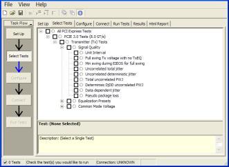
10 CEM 4.0 and Compliance Testing CEM 4.0 currently at v0.5. V0.7 in CEM Review (Jan 2017) PCIe 4.0 Compliance Requirements CEM Spec completion at v0.7 (v0.9 optimal) Completion of Test Specifications Config Test Spec Link Transaction Test Spec System Firmware (BIOS) Test Spec Electrical Test Spec Retimer Test Spec Availability of Gen4 Compliance Test Fixtures for Purchase Preliminary PCIe 4.0 Test Fixtures to debut at April 2017 Workshop Estimated Schedule First Gen4 FYI testing commences April 2017 Official FYI Testing to begin late 2017 Official Integrators list test to start mid 2018 PCIe GT/s TX/RX Testing Page 10
11 PCI Express 4.0 Keysight Total Solution Physical layer interconnect design Physical layertransmitter test Physical layerreceiver test ADS design software X, Z-Series oscilloscope M8020A J-BERT High Perfformance BERT 86100D DCA-J/TDR N5393F PCI Express electrical compliance software N5990A automated compliance and device characterization test software E5071C ENA option TDR 86100CU-400 PLL and Jitter Spectrum Measurement SW Industry s lowest scope noise floor/sensitivity and trigger jitter DSA-X Series & Q Series Real-Time Oscilloscopes Automated compliance software accurate, efficient and consistent PCIe GT/s TX/RX Testing Page 11
12 PCIe 4.0 TX Testing PCIe GT/s TX/RX Testing Page 12

13 PCIe 4.0 v0.9 Finalizes TX Scope Bandwidth Requirement Gen4 De-embed limit Gen4 Scope BW limit PCIe GT/s RX Testing Page 13


14 PCI Express 4.0 TX Measurement Basic Test Setup BASE Spec (v0.7) Keysight Z-Series Real Time Oscilloscope PCIe 4.0 ASIC/IC Custom Breakout Board S-Parameters of Replica Ch. Used to de-embed to pin. PCIe GT/s RX Testing Page 14
15 N5393F/G New Features Supports PCIe 4.0 BASE TX Testing at 2.5G, 5G, 8G and 16GT/s (v0.7 BASE) Supports PCIe 4.0 Reference Clock tests (2.5G, 5G, 8G, 16G) Supports U.2 (SFF-8639) CEM tests for endpoints and root complexes (2.5G, 5G, 8G). Automated DUT control using an 81150/60A Pulse Generator ARB. Enhanced Switch Matrix supporting arbitrary lane mapping New Workshop Compliance Mode for rapid PCISIG official compliance testing. PCIe GT/s RX Testing PCIe GT/s TX Testing Page 15
 TX N5393F Test Application New Test Plan")

16 Keysight PCIe 4.0 (Gen4) TX N5393F Test Application New Test Plan Setup Select Speeds of Gen4 Device to Test Select Standard Version to Test Automatic DUT control for toggle signal PCIe GT/s TX Testing Page 16
 TX N5393F Test Application Select a complete Gen4 TX")
17 Keysight PCIe 4.0 (Gen4) TX N5393F Test Application Select a complete Gen4 TX test plan. PCIe GT/s TX Testing Page 17
 TX N5393F Test Application Use InfiniiSim for")

18 Keysight PCIe 4.0 (Gen4) TX N5393F Test Application Use InfiniiSim for de-embedding with optional N5465A Select InfiniiSim under Tools Choose your de-embed transfer function Fine-tune your de-embed filter (bandwidth, etc) PCIe GT/s TX Testing Page 18
19 Consolidated Jitter Parameters for ALL data rates 19 Note Gen1, Gen2 Jitter now has same measurement parameter as Gen3/4 but different values. Symbol V TX-BOOST-RS EQ TX-COEFF-RES V TX-DE-RATIO- 3.5dB V TX-DE-RATIO-6dB T TX-UTJ T TX-UTJ-SRIS T TX-UDJDD T TX-UPW-TJ T TX-UPWDJDD Maximum nominal Tx boost ratio for reduced swing Tx coefficient resolution Tx de-emphasis ratio for 2.5 and 5 G Tx de-emphasis ratio for 5 G Tx uncorrelated total jitter Tx uncorrelated total jitter when testing for the IR clock mode with SSC Tx uncorrelated Dj for non-embedded Refclk Total uncorrelated pulse width jitter Deterministic DjDD uncorrelated pulse width jitter T TX-RJ Tx Random jitter N/A L TX-SKEW RL TX-DIFF RL TX-CM Parameter description Lane-to-Lane Output Skew Tx package plus die differential return loss Tx package plus die common mode return loss 2.5 GT/s 5.0 GT/s 8.0 GT/s 16.0 GT/s Units Notes N/A N/A 2.5 ~2.5 (min) db Assumes ±1.0 db tolerance from diagonal elements in Table 9-3. N/A N/A 1/24 (max) 1/63 (min) 3.0 (min) 4.0 (max) 3.0 (min) 4.0 (max) 1/24 (max) 1/63 (min) N/A N/A N/A db N/A 5.5 (min) 6.5 (max) N/A N/A db 100 (max) 50 (max) (max) 12.5 (max) ps PP at (max) (max) (max) (max) ps PP at See Sec for details. See Sec for details. 100 (max) 30 (max) 12 (max) 6.25 (max) ps PP See Sec for details. N/A 40 (max) 24 (max) 12.5 (max) ps PP at See Sec for details N/A 40 (max) 10 (max) 5 (max) ps PP See Sec for details ps RMS Informative parameter only. Range of Rj possible with zero to maximum CDR SRIS 8GG, allowed 16G T TX- UDJDD. 2.5 (max) 2.0 (max) 1.5 (max) 1.25 (max) ns Between any two Lanes within a single Transmitter. See Figure 9-19 See Figure 9-20 See Figure 9-19 See Figure 9-20 See Figure 9-19 See Figure 9-20 See Figure 9-19 See Figure 9-20 db Note 6 db Note 6 Page
20 PCIe 4.0 Reference Clock Testing PCIe GT/s TX Testing Page 20
21 PCIe 4.0 Reference Clock AC Parameters Symbol Table 2-1: REFCLK DC Specifications and AC Timing Requirements Parameter 100 MHz Input Rising Edge Rate Rising Edge Rate V/ns 2, 3 Falling Edge Rate Falling Edge Rate V/ns 2, 3 VIH Differential Input High Voltage +150 mv 2 VIL Differential Input Low Voltage -150 mv 2 VCROSS Absolute crossing point voltage mv 1, 4, 5 VCROSS DELTA Variation of VCROSS over all rising clock edges +140 mv 1, 4, 9 VRB Ring-back Voltage Margin mv 2, 12 TSTABLE Time before VRB is allowed 500 ps 2, 12 TPERIOD AVG Average Clock Period Accuracy ppm 2, 10, 13 TPERIOD ABS Absolute Period (including Jitter and Spread Spectrum modulation) ns 2, 6 TCCJITTER Cycle to Cycle jitter 150 ps 2 VMAX Absolute Max input voltage V 1, 7 VMIN Absolute Min input voltage V 1, 8 Duty Cycle Duty Cycle % 2 Rising edge rate (REFCLK+) to Rise-Fall falling edge rate (REFCLK-) 20 % 1,14 Matching matching ZC-DC Clock source DC impedance , 11 Min Max Unit Note 21 Standard Reference Clock Test Fixture for ALL data rate independent and data rate dependent parameters. PCIe GT/s TX Testing Page
22 PCIe 4.0 Phase Jitter Parameters Jitter Limits for Refclk Architectures Table 9-18 lists the jitter limits for the CC Refclk architecture at each of the four data rates Jitter at 2.5 GT/s is measured as a peak to peak jitter value, because a substantial proportion of the jitter is SSC harmonics which appears at the receiver as Dj. The combination of the 2.5 GT/s PLL and CDR bandwidths passes a significant amount of SSC residual, where it appears Dj. The 108 ps number is the same as that specified in the 3.0 CEM spec. For 5.0, 8.0, and 16.0 GT/s jitter is specified as an RMS (Rj) value. These signaling speeds utilize a lower PLL BW and a higher CDR BW, and the effect is to suppress SSC harmonics such that almost all the jitter appears as Rj. Data Rate CC jitter Limit Notes 2.5G 108 ps pp 1, 2 5.0G 3.1 ps RMS 1, 2 8.0G 1.0 ps RMS 1, 2 16G Table 9-18: Jitter Limits for CC Architecture 0.5 ps RMS Note that.7 ps RMS is to be used in channel simulations to account for additional noise in a real system. Note: 1. The Refclk jitter is measured after applying the filter function in Figure Jitter measurements shall be made with a capture of at least 100,000 clock cycles captured by a real time oscilloscope with a sample rate of 20 GS/s or great. Broadband oscilloscope noise must be minimized in the measurement. 1,2 Standard Reference Clock Test Fixture for Phase Jitter Parameters 22 PCIe GT/s TX Testing Page
23 Reference Clock for Gen4 PLL 1 PLL 2 Table 9-17: Common Refclk PLL and CDR Characteristics for 8.0 and 16.0 GT/s Show Spec in Report PLL #1 PLL # db peaking 1.0 db peaking 0.01 db peaking 3.0 db peaking BW PLL (min) = 5.0 MHz BW PLL (max) = 16 MHz w n1 = 1.12 Mrad/s z 1 = 14 w n1 = 3.58 Mrad/s z 1 = 14 w n1 = Mrad/s z 1 = 1.16 w n1 = Mrad/s z 1 = 1.16 BW PLL (min) = 8.0 MHz BW PLL (max) = 16 MHz w n2 = 1.79 Mrad/s z 2 = 14 w n2 = 3.58 Mrad/s z 2 = 14 w n2 = Mrad/s z 2 = 0.54 w n2 = Mrad/s z 2 = 0.54 BW CDR (min) = 5 MHz, 1 st order 64 combinations 5 GT/s REF Clock 8G TX Phase Jitter PLL1 PLL 2 ATX BTX CTX DTX ATX BTX CTX DTX ARX BRX CRX 0.3 ps 7.9ps 0.99 DRX ARX BRX CRX DRX If user right clicks on a curve, pop up menu shows curves related to the calculation of that value. Color code fields for PASS/Fail/Margin PCIe GT/s TX/RX Testing Report Results in a Matrix Page 23
 TX N5393F Test Application Gen4 Reference Clock Tests Common 100MHz AC Parameters Phase")
24 Keysight PCIe 4.0 (Gen4) TX N5393F Test Application Gen4 Reference Clock Tests Common 100MHz AC Parameters Phase Jitter tests for 2.5G, 5G, 8G, and 16G SSC Clock Tests PCIe GT/s TX Testing Page 24
25 PCIe 3.0 U.2 Testing (SFF-8639) PCIe GT/s TX Testing Page 25

26 The U.2 Connector Pinout PCIe GT/s TX Testing Page 26

27 New U.2 CBB Fixtures to be made available from PCI-SIG PCIe GT/s TX Testing Page 27

28 Data and Clock Connections to U.2 connector on Backplane Refclk Connection Data Connection 28 PCIe GT/s TX Testing Page
 TX N5393F Test")

29 Keysight PCIe 4.0 (Gen4) TX N5393F Test Application U.2 Test Setup U.2 Test Selection for Endpoint Card PCIe GT/s RX Testing Page 29
30 Speeding up Testing Automated DUT Control Enhanced Switch Matrix Lane Mapping Workshop Compliance Mode PCIe GT/s RX Testing PCIe GT/s TX Testing Page 30


31 Keysight PCIe 4.0 (Gen4) TX N5393F*Test Application For use with PCIe 3.0 and below. Use and 81150A or 81160A to Generate the CBB Compliance Toggle signal to toggle your DUT between the different compliance states. Control DUT automatically to switch compliance toggle modes Workshop compliance mode is used for PCISIG compliance testing and uses Sigtest to test your DUT as well as to create PCISIG Compliance test reports. You specify what directory to use for your Workshop Compliance Mode (Sigtest generated) HTML reports along with data files PCIe GT/s RX Testing Page 31
 TX N5393F*Test Application Connection Options Choose from available switch matrix")

32 Keysight PCIe 4.0 (Gen4) TX N5393F*Test Application Connection Options Choose from available switch matrix options for multi-lane testing If you don t have a switch, you can test using all four scope channels to test two lanes with one setup. Select Lanes to map to your switch network setup Lanes to test can be chosen arbitrarily. PCIe GT/s RX Testing Page 32
 TX N5393F*Test Application Test Automation and Connection Example 81150A used for DUT control (toggle pulse to switch compliance states) Scope")
33 Keysight PCIe 4.0 (Gen4) TX N5393F*Test Application Test Automation and Connection Example 81150A used for DUT control (toggle pulse to switch compliance states) Scope configured for Root Complex Testing Root Complex DUT being tested for PCISIG Compliance Keysight U3020A Switch Matrix PCIe GT/s RX Testing Page 33


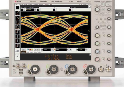
34 PCIe 4.0 Receiver Testing at 16Gbps >16Gbps BERT Link Equalization Jitter and De-emphasis PCIe GT/s RX Testing Page 34
35 Differences between PCIe 3 and PCIe 4 PCIe 3.0/3.1 PCIe 4.0 rev 0.5 PCIe 4.0 rev 0.7 added transfer rate 8 GT/s 16 GT/s coding block alignment & scrambler reset 128B/130B EIEOS for block alignment EIEOS 10 00FF 00FF 00FF 00FF 00FF 00FF 00FF 00FF 500 MHz scrambling 10 00FF 00FF 00FF 00FF 00FF 00FF 00FF 00FF 1 GHz control: no (partially), data: always PRBS ; scrambler reset through EIEOS FFFF 0000 FFFF 0000 FFFF 0000 FFFF 500 MHz Adaptable TX link equalization yes yes, two step process: first 8G link eq followed by 16G link eq if 8G link eq is successful RX tests stressed jitter test and stressed voltage test one RX stress test rssc for common reference clock no no yes eye opening after reference RX for stress signal cal 0.3 UI, 25 mv, BER of UI, 15 mv (RX eye spec. is actually 14 mv), BER of stress signal adjustment using RJ, DM-SI and V diff coarse: ISI fine: DM-SI + SJ or DM-SI + V diff CTLE pole 1 frequency 2 GHz 4 GHz 2 GHz Channel for RX test No connector required PCIe 4.0 CEM connector required as part of RX test channel Page
36 Differences between PCIe 3 and PCIe 4 Relevant changes with PCIe 4.0 rev 0.5 and 0.7 PCIe 3.0/3.1 PCIe 4.0 rev 0.5 PCIe 4.0 rev 0.7 added transfer rate 8 GT/s 16 GT/s coding block alignment & scrambler reset 128B/130B EIEOS for block alignment EIEOS 10 00FF 00FF 00FF 00FF 00FF 00FF 00FF 00FF 500 MHz scrambling Link EQ gets more important 10 00FF 00FF 00FF 00FF 00FF 00FF 00FF 00FF 1 GHz control: no (partially), data: always PRBS ; scrambler reset through EIEOS FFFF 0000 FFFF 0000 FFFF 0000 FFFF 500 MHz Adaptable TX link equalization yes yes, two step process: first 8G link eq followed by 16G link eq if 8G link eq is successful RX tests stressed jitter test and stressed voltage test one RX stress test rssc for common reference clock no no yes eye opening after reference RX for stress signal cal Different cal procedure 0.3 UI, 25 mv, BER of UI, 15 mv (RX eye spec. is actually 14 mv), BER of stress signal adjustment using RJ, DM-SI and V diff coarse: ISI fine: DM-SI + SJ or DM-SI + V diff Reference CTLE changes: pole 1 frequency affects RX cal Special cal channel fixture required 2 GHz 4 GHz 2 GHz Channel for RX test No connector required PCIe 4.0 CEM connector required as part of RX test channel Page
37 Differences between PCIe 3 and PCIe 4 Relevant changes between PCIe 4.0 rev 0.5 to rev 0.7 PCIe 3.0/3.1 PCIe 4.0 rev 0.5 PCIe 4.0 rev 0.7 added transfer rate 8 GT/s 16 GT/s coding Affects block alignment and descrambler reset block alignment & scrambler reset 128B/130B EIEOS for block alignment EIEOS 10 00FF 00FF 00FF 00FF 00FF 00FF 00FF 00FF 500 MHz scrambling A new type of impairment. Amplitude is significantly higher compared to PCIe FF 00FF 00FF 00FF 00FF 00FF 00FF 00FF 1 GHz control: no (partially), data: always PRBS ; scrambler reset through EIEOS FFFF 0000 FFFF 0000 FFFF 0000 FFFF 500 MHz Adaptable TX link equalization yes yes, two step process: first 8G link eq followed by 16G link eq if 8G link eq is successful RX tests stressed jitter test and stressed voltage test one RX stress test rssc for common reference clock no no yes Impacts RX stress test calibration eye opening after reference RX for stress signal cal 0.3 UI, 25 mv, BER of UI, 15 mv (RX eye spec. is actually 14 mv), BER of stress signal adjustment using RJ, DM-SI and V diff coarse: ISI fine: DM-SI + SJ or DM-SI + V diff Reference CTLE changes: pole 1 frequency 2 GHz 4 GHz 2 GHz Channel for RX test No connector required PCIe 4.0 CEM connector required as part of RX test channel Page
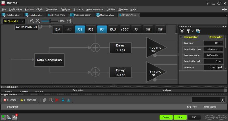
38 Blub AIC Test System Test EQ starts EQ complete Dynamic Link Equalization Handshake 8G The four phases of the Link Equalization Protocol RcvrLock Phase 0 Phase 1 Phase 2 UPSTREAM PORT Add-In Card J-BERT M8020A TS1, [P2] EC = 00b, PV = P2 TS1, [P2] EC = 01b, PV = P2, Use_Preset = 0 TS1, [P2] EC = 10b, PV = P3, Use_Preset = 1 TS1, [P2] EC = 10b, PV = P4, Use_Preset = 1 BER < Phase 3 TS1, [P2] EC = 11b, PV = P2, Use_Preset = 0 TS1, [P6] EC = 11b, PV = P6, Use_Preset = 0 TS1, [P7] EC = 11b, PV = P7, Use_Preset = 0 RcvrLock TS1, [P7] EC = 00b, PV = P7 EQTS2 PV = P1 DOWNSTREAM PORT J-BERT M8020A System TS1, [P1] EC = 01b, PV = P1, Use_Preset = 0 TS1, [P1] EC = 10b, PV = P1, Use_Preset = 0 TS1, [P3] EC = 10b, PV = P3, Use_Preset = 0 TS1, [P4] EC = 10b, PV = P4, Use_Preset = 0 TS1, [P4] EC = 11b, PV = P6, Use_Preset = 1 TS1, [P4] EC = 11b, PV = P7, Use_Preset = 1 TS1, [P4] EC = 00b, PV = P4, Use_Preset = 0 RcvrLock Phase 1 Phase 2 Phase 3 BER < RcvrLock PV EC Phase 0: 2.5 Gb/s Downstream port tells upstream port which initial preset to use after the speed change will have been done. Phase 1: 8 Gb/s Link partners settle on 8 GT/s speed. Exchange FS/LF values. Phase 2: 8 Gb/s Add-in Card sets up the deemphasis of the System Board s transmitter. Phase 3: 8 Gb/s System Board sets up the deemphasis of the Add-in Card s transmitter. Preset Value Equalization Control PCIe GT/s RX Testing Page 38
39 Blub AIC Test System Test EQ starts EQ complete Dynamic Link Equalization Handshake 16G The four phases of the Link Equalization Protocol RcvrLock Phase 0 Phase 1 Phase 2 UPSTREAM PORT Add-In Card J-BERT M8020A TS1, [P2] EC = 00b, PV = P2 TS1, [P2] EC = 01b, PV = P2, Use_Preset = 0 TS1, [P2] EC = 10b, PV = P3, Use_Preset = 1 TS1, [P2] EC = 10b, PV = P4, Use_Preset = 1 BER < Phase 3 TS1, [P2] EC = 11b, PV = P2, Use_Preset = 0 TS1, [P6] EC = 11b, PV = P6, Use_Preset = 0 TS1, [P7] EC = 11b, PV = P7, Use_Preset = 0 RcvrLock TS1, [P7] EC = 00b, PV = P7 EQTS2 PV = P1 DOWNSTREAM PORT J-BERT M8020A System TS1, [P1] EC = 01b, PV = P1, Use_Preset = 0 TS1, [P1] EC = 10b, PV = P1, Use_Preset = 0 TS1, [P3] EC = 10b, PV = P3, Use_Preset = 0 TS1, [P4] EC = 10b, PV = P4, Use_Preset = 0 TS1, [P4] EC = 11b, PV = P6, Use_Preset = 1 TS1, [P4] EC = 11b, PV = P7, Use_Preset = 1 TS1, [P4] EC = 00b, PV = P4, Use_Preset = 0 RcvrLock Phase 1 Phase 2 Phase 3 BER < RcvrLock PV EC Phase 0: 2.5 Gb/s Downstream port tells upstream port which initial preset to use after the speed change will have been done. Phase 1: 8 Gb/s Link partners settle on 8 GT/s speed. Exchange FS/LF values. Phase 2: 8 Gb/s Add-in Card sets up the deemphasis of the System Board s transmitter. Phase 3: 8 Gb/s System Board sets up the deemphasis of the Add-in Card s transmitter. Preset Value Equalization Control IF SUCCESSFUL Phase 1: 16 Gb/s Link partners settle on 16 GT/s speed. Exchange FS/LF values. Phase 2: 16 Gb/s Add-in Card sets up the deemphasis of the System Board s transmitter. Phase 3: 16 Gb/s System Board sets up the deemphasis of the Add-in Card s transmitter. PCIe GT/s RX Testing Page 39

40 PCIe 4.0 RX Tests 16 GT/s Base Specification RX Test Setup PCIe 4.0 Base Spec requires a CEM connector to be part of the test channel! All other impairments are provided by J-BERT M8020A A built-in reference clock multiplier enables J-BERT M8020A to operate on a DUT s reference clock if required No ref clock connection in case of IR / SRIS PCIe GT/s RX Testing Page 40


41 PCIe 4.0 Calibration Channel Example (PCISIG) CEM Connector. 85ohm Differential Impedance PCIe GT/s TX/RX Testing Page 41
42 PCIe 4.0 RX Tests 16 GT/s Base Specification RX SJ Mask Different jitter tolerance curves for CC and IR rssc for CC only Constant 33 khz SJ tone in addition to jitter tolerance curve and 210 MHz SJ tone for IR only PCIe GT/s RX Testing Page 42


43 PCIe 4.0 RX Tests Test Automation Support for CC as well as IR End point as well as root complex 2.5 GT/s, 5 GT/s, 8 GT/s and 16 GT/s Contact Keysight for availability PCIe GT/s RX Testing Page 43


44 PCIe 4.0 RX Stress Signal Calibration 16 GT/s Receiver Stress Signal Calibration Setup 1 V diff, pre-shoot and de-emphasis calibration N5990A Test Automation SW for PCIe RJ calibration SJ calibration PCIe GT/s RX Testing Page 44


45 PCIe 4.0 RX Stress Signal Calibration 16 GT/s Receiver Stress Signal Calibration Setup 2 N5990A Test Automation SW for PCIe PCIe Base Specification 4.0 requires a CEM connector to part of the test channel! PCIe 4.0 Base Spec requires a CEM connector to be part of the test channel Channel calibration with preset selection to get as close to target eye height and eye width as possible. J-BERT M8020A s internal ISI can be used to calibrate channel. Preset is selected on optimal RX eye area DM-SI and CM-SI are calibrated through the channel Compliance eye calibration is done by adjusting DM-SI, SJ or V diff If SJ was changed from 100 mui during the compliance eye calibration, the SJ portion >100 mui is applied as a secondary SJ 210 MHz during the RX test. This allows to follow the jitter tolerance compliance curve PCIe GT/s RX Testing Page 45
46 PCIe 4.0 RX Stress Signal Calibration Channel Calibration Channel closest to 28dB 8GHz is chosen initially Optimal preset is chosen for channel setting based on RX eye area after reference RX Insertion loss of channel is varied to get close to target eye height and target eye width Reference RX eq is optimized by analysis SW for each channel + preset combination Too many steps for manual procedure PCIe GT/s RX Testing Page 46

47 PCIe 4.0 RX Stress Signal Calibration Compliance Eye Calibration Channel determined by the channel calibration is applied DM-SI, SJ and V diff are adjusted to find correct combination for a compliant eye of the reference RX PCIe GT/s RX Testing Page 47
48 Conclusions 1. Gen4 is at the 0.7 release version and work is underway on v0.9. Most of the hard work has been done but it is important for the SIG to ensure the details are captured. 2. Official statement on scope BW required for TX and RX calibration is in the v0.9 spec. The official requirement is a minimum scope bandwidth of 25GHz due to the need to match edge BW of JBERT during calibration. This also is required for TX testing. 3. PCIe 4.0 Reference Clock Phase Jitter requirements have expanded significantly since PCIe Official U.2 fixtures from the PCISIG are now available (SFF-8639) 5. Receiver Calibration Channel is to have a CEM connector EIEOS goes to 16 1 s and 16 0s at v PCIe 4.0 informal FYI testing (CEM) will begin at the April workshop in Milpitas. 7. Tools for full PCIe 4.0 TX and RX BASE testing are available today. Keysight has the only demonstrated Gen4 capable, protocol aware BERT for RX testing at 16GT/s. PCIe GT/s TX/RX Testing Page 48
49 PCI Express 4.0 Keysight Total Solution Physical layer interconnect design ADS design software 86100D DCA-J/TDR E5071C ENA option TDR Industry s lowest scope noise floor/sensitivity and trigger jitter PCIe GT/s TX/RX Testing Page 49
50 PCI Express 4.0 Keysight Total Solution Physical layer interconnect design Physical layertransmitter test ADS design software X, Z-Series oscilloscope 86100D DCA-J/TDR N5393F PCI Express electrical compliance software E5071C ENA option TDR 86100CU-400 PLL and Jitter Spectrum Measurement SW Industry s lowest scope noise floor/sensitivity and trigger jitter DSA-X Series & Q Series Real-Time Oscilloscopes PCIe GT/s TX/RX Testing Page 50

51 PCI Express 4.0 Keysight Total Solution Physical layer interconnect design Physical layertransmitter test Physical layerreceiver test ADS design software X, Z-Series oscilloscope M8020A J-BERT High Perfformance BERT 86100D DCA-J/TDR N5393F PCI Express electrical compliance software N5990A automated compliance and device characterization test software E5071C ENA option TDR 86100CU-400 PLL and Jitter Spectrum Measurement SW Industry s lowest scope noise floor/sensitivity and trigger jitter DSA-X Series & Q Series Real-Time Oscilloscopes Automated compliance software accurate, efficient and consistent PCIe GT/s TX/RX Testing Page 51
52 For more Information You will find more information on PCI Express and Keysight test solutions at: PCI-SIG Website, Specification, S/W Tools, Keysight Test Procedure Keysight tools to help you succeed with your PCI Express design such as the N5393F Compliance application. Keysight digital webcast registration page. PCIe 4.0 Rx Test Detailed Information Rick Eads Principal PCI Express Planner PCIe GT/s RX Testing Page 52

53 Invitation to Join PCI-SIG Group on Linked-In* Must be employed by a member company of the PCI-SIG to join. PCIe GT/s TX/RX Testing Page 53
Advanced Techniques for Validating PCI Express 4.0 Transmitters and Receivers Rick Eads Principal PCIe Tools Planner Keysight Technologies
 Advanced Techniques for Validating PCI Express 4.0 Transmitters and Receivers Rick Eads Principal PCIe Tools Planner Keysight Technologies Page Agenda PCIe 4.0 Ecosystem and Timeline PCIe 4.0 TX Testing
PCI Express Link Equalization Testing 서동현
 PCI Express Link Equalization 서동현 Application Engineer January 19th, 2016 Agenda Introduction Page 2 Dynamic Link Equalization TX/RX Link Equalization Tests Test Automation RX Stress Signal Calibration
PCI Express 3.0 Characterization, Compliance, and Debug for Signal Integrity Engineers
 PCI Express 3.0 Characterization, Compliance, and Debug for Signal Integrity Engineers - Transmitter Testing - Receiver Testing - Link Equalization Testing David Li Product Marketing Manager High Speed
Agilent. Master your next PCIe test with the Agilent M8020A High-Performance BERT Application Brief
 Agilent Master your next PCIe test with the Agilent M8020A High-Performance BERT Application Brief 1 Table of Contents Contents Disclaimer... 3 1 Introduction... 4 2 PCI Express Specifications... 4 3 PCI
PCI Express 4.0. Electrical compliance test overview
 PCI Express 4.0 Electrical compliance test overview Agenda PCI Express 4.0 electrical compliance test overview Required test equipment Test procedures: Q&A Transmitter Electrical testing Transmitter Link
Successfully negotiating the PCI EXPRESS 2.0 Super Highway Towards Full Compliance
 the PCI EXPRESS 2.0 Super Highway Towards Full Compliance Page 1 Agenda Introduction PCIe 2.0 changes from 1.0a/1.1 Spec 5GT/s Challenges Error Correction Techniques Test tool and fixture changes Agilent
Achieving PCI Express Compliance Faster
 Achieving PCI Express Compliance Faster Agenda PCIe Overview including what s new with Gen4 PCIe Transmitter Testing PCIe Receiver Testing Intro to Tektronix s PCIe Tx and Rx Test Solution PCIe Market
PCIe 3.0 Compliance Testing Dan Froelich Serial Enabling Workgroup Co-Chair
 PCIe 3.0 Compliance Testing Dan Froelich Serial Enabling Workgroup Co-Chair Copyright 2015, PCI-SIG, All Rights Reserved 1 Agenda PCIe Compliance Program Status PCIe Compliance Process Compliance Test
PCI Express Rx-Tx-Protocol Solutions
 PCI Express Rx-Tx-Protocol Solutions Customer Presentation December 13, 2013 Agenda PCIe Gen4 Update PCIe Gen3 Overview PCIe Gen3 Tx Solutions Tx Demo PCIe Gen3 Rx Solutions Rx Demo PCIe Gen3 Protocol
COMPLIANCE STATEMENT
 COMPLIANCE STATEMENT Specification Specification name: PCIE-BASE-REV4.-CC-REFCLK Specification title: Common-clock Refclk Evaluation for PCIe v4. BASE (v1.) Specification owner: JitterLabs Device Under
5 GT/s and 8 GT/s PCIe Compared
 5 GT/s and 8 GT/s PCIe Compared Bent Hessen-Schmidt SyntheSys Research, Inc. Copyright 2008, PCI-SIG, All Rights Reserved 1 Disclaimer The material included in this presentation reflects current thinking
Master your next PCIe test PCI Express J-BERT M8020A High-Performance BERT. Application Brief
 Master your next PCIe test PCI Express J-BERT M8020A High-Performance BERT Application Brief Table of Contents Revision History 3 Disclaimer 3 1 Introduction 4 2 PCI Express Specifications 4 3 PCI Express
R&S RTO-K81, R&S RTP-K81 PCIe Compliance Test Test Procedures
 PCIe Compliance Test Test Procedures (=QFñ2) 1333229902 Test Procedures Version 03 This manual describes the PCIe compliance test procedures with the following options: R&S RTO-K81 (1326.0920.02) - PCIe
PCI Express Electrical Basics
 PCI Express Electrical Basics Dean Gonzales Advanced Micro Devices Copyright 2015, PCI-SIG, All Rights Reserved 1 Topics PCI Express Overview Enhancements for 8GT/s Target Channels for the Specification
PCI Express 3.0CEM Stressed Eye Calibration and Receiver Testing
 PCI Express 3.0CEM Stressed Eye Calibration and Receiver Testing Methods of Implementation using Tektronix BERTScope BSA85C Analyzer, CR125A Clock Recovery, DPP125B De-Emphasis Processor, and Series 70000
DisplayPort 1.4 Webinar
 DisplayPort 1.4 Webinar Test Challenges and Solution Yogesh Pai Product Manager - Tektronix 1 Agenda DisplayPort Basics Transmitter Testing Challenges DisplayPort Type-C Updates Receiver Testing Q and
Simplifying Validation and Debug of USB 3.0 Designs - Tektronix USB Testing Solutions Introduction. name title
 Simplifying Validation and Debug of USB 3.0 Designs - Tektronix USB Testing Solutions Introduction name title Agenda Introduction USB 3.0 SuperSpeed Why USB 3.0? Timeline Cable Transmitter Receiver Protocol
RT-Eye PCI Express Compliance Module Methods of Implementation (MOI)
") Technical Reference RT-Eye PCI Express Compliance Module Methods of Implementation (MOI) 071-2041-00 www.tektronix.com Copyright Tektronix. All rights reserved. Licensed software products are owned by
Technical Reference RT-Eye PCI Express Compliance Module Methods of Implementation (MOI) 071-2041-00 www.tektronix.com Copyright Tektronix. All rights reserved. Licensed software products are owned by
PCI Express TM Architecture. PHY Electrical Test Considerations Revision 1.1
 PCI Express TM Architecture PHY Electrical Test Considerations Revision 1.1 February 2007 i PHY ELECTRICAL TEST CONSIDERATIONS, REVISION 1.1 REVISION REVISION HISTORY DATE 1.0 Initial Release. 4/26/2004
Raj Kumar Nagpal, R&D Manager Synopsys. Enabling Higher Data Rates and Variety of Channels with MIPI D-PHY
 Raj Kumar Nagpal, R&D Manager Enabling Higher Data Rates and Variety of Channels with MIPI D-PHY Agenda Design motivation MIPI D-PHY evolution Summary of MIPI D-PHY specification MIPI channel evolution
Virtex-6 FPGA GTX Transceiver Characterization Report
 Virtex-6 FPGA GTX Transceiver Characterization Report PCI Express 2.0 (2.5 and 5.0 Gb/s) Electrical Standard Xilinx is disclosing this user guide, manual, release note, and/or specification (the Documentation
Tektronix Innovation Forum
 Tektronix Innovation Forum Enabling Innovation in the Digital Age DisplayPort 1.2 Spec Updates and overview of Physical layer conformance testing Presenter: John Calvin DisplayPort 1.2 Spec Updates Agenda
Technical Reference. Version 4.8. DPOJET Opt. PCE, PCE3, PCE4 PCI Express Measurements & Setup Library
 Technical Reference DPOJET Opt. PCE, PCE3, PCE4 PCI Express Measurements & Setup Library Methods of Implementation (MOI) for Verification, Debug and Characterization Version 4.8 077-0267-01 www.tek.com
PCI Gen3 (8GT/s) Receiver Test
 Receiver Test") PCI Gen3 (8GT/s) Receiver Test Tektronix MOI for PCIe Gen3 (8GT/s) Receiver Jitter Tolerance Test (Add-In Card and System) using BSX Series BERTScope Bit Error Tester and BERTScope PCIE3.0 Receiver Testing
PCI Gen3 (8GT/s) Receiver Test Tektronix MOI for PCIe Gen3 (8GT/s) Receiver Jitter Tolerance Test (Add-In Card and System) using BSX Series BERTScope Bit Error Tester and BERTScope PCIE3.0 Receiver Testing
Compliance test method and detailed spec for -USB3.0. Tektronix Korea YJ.PARK
 Compliance test method and detailed spec for -USB3.0 Tektronix Korea YJ.PARK Differences from USB2.0 High-Speed 480MT/s No-SSC 2 wires for signaling Tx and Rx use the same wire 1 bi-directional link DC
Agilent N5393C PCI Express Automated Test Application
 Agilent N5393C PCI Express Automated Test Application Compliance Testing Methods of Implementation Agilent Technologies Notices Agilent Technologies, Inc. 2004-2010 No part of this manual may be reproduced
DisplayPort Testing Challenges
 DisplayPort Testing Challenges U N Vasudev May 6 th 2013 Agenda DisplayPort Overview DisplayPort 1.2 updates DisplayPort 1.2 Transmitter Testing What s New: T2, TP3, TP3EQ Physical Layer Test Overview
PCI Express 4.0 Test Solution
 PCI Express 4.0 Test Solution Key Features PCIe Gen4 CEM compliance testing: Transmitter preset and signal quality Transmitter link equalization Receiver test calibration Receiver jitter tolerance Fully
N1014A SFF-8431 (SFP+)
") DATA SHEET N1014A SFF-8431 (SFP+) Compliance and Debug Application for 86100D DCA-X and N109X DCA-M Oscilloscopes Be Confident With Compliant Measurements Easy-to-use oscilloscope application that lets
DATA SHEET N1014A SFF-8431 (SFP+) Compliance and Debug Application for 86100D DCA-X and N109X DCA-M Oscilloscopes Be Confident With Compliant Measurements Easy-to-use oscilloscope application that lets
High Speed Design Testing Solutions
 High Speed Design Testing Solutions - Advanced Tools for Compliance, Characterization and Debug name title Agenda High-Speed Serial Test Challenges High-Speed Serial Test Simplified - Characterization
QPHY-PCIE3 Operator s Manual
 QPHY-PCIE3 Operator s Manual Revision B November, 2017 Relating to: XStreamDSO Version 8.5.x.x QualiPHY Version 8.5.x.x 700 Chestnut Ridge Road Chestnut Ridge, NY, 10977-6499 Tel: (845) 425-2000, Fax:
PCI Express Transmitter Compliance and Debug
 PCI Express Transmitter Compliance and Debug PCE3 Datasheet Features & Benefits PCIe Test Support: Supports Compliance and Validation of PCIe Gen1/2/3 Interfaces based on PCIe Base and CEM Specifications
10 THINGS TO KNOW ABOUT PCIe. ebook
 10 THINGS TO KNOW ABOUT ebook Overview PCI Express () is a high performance, general purpose I/O interconnect used in a wide variety of computing and communications products. There is a high degree of
Keysight N5393F/G PCI Express 4.0 (Gen4) Software for Infiniium Oscilloscopes. Data Sheet
 Software for Infiniium Oscilloscopes. Data Sheet") Keysight N5393F/G PCI Express 4.0 (Gen4) Software for Infiniium Oscilloscopes Data Sheet 02 Keysight N5393F/G PCI Express 4.0 (Gen4) Software for Infiniium Oscilloscopes - Data Sheet Table of Contents
Keysight N5393F/G PCI Express 4.0 (Gen4) Software for Infiniium Oscilloscopes Data Sheet 02 Keysight N5393F/G PCI Express 4.0 (Gen4) Software for Infiniium Oscilloscopes - Data Sheet Table of Contents
PCI Express 3.0 Testing Approaches for PHY and Protocol Layers
 PCI Express 3.0 Testing Approaches for PHY and Protocol Layers Agenda Introduction to PCI Express 3.0 Trends and Challenges Physical Layer Testing Overview Transmitter Design & Validation Transmitter Compliance
PCI Express Application Software
 PCI Express Application Software PCE3 and PCE Data Sheet PCE (Supports Gen 1/2) PCI Express 1.0 and 2.0 Characterization, Debug, and Compliance Testing Automated Measurements for PCI Express 1.x and 2.0
Provides information for this release. Describes added functions for this release. Describes bug fixes in the released software version.
 ANRITSU CORPORATION 5-1-1 Onna, Atsugi-shi, Kanagawa 243-8555 Japan Anritsu - GRL PCIe 4.0 CEM Rx Test Application Release Note First Edition This software is released for PCIe CEM Rx Test. Table of Contents
QPHY-PCIE3-TX-RX Operator s Manual
 QPHY-PCIE3-TX-RX Operator s Manual Revision C November, 2017 Relating to: XStreamDSO Version 8.5.x.x QualiPHY Version 8.5.x.x 700 Chestnut Ridge Road Chestnut Ridge, NY, 10977-6499 Tel: (845) 425-2000,
PCI Express 1.0a and 1.1 Add-In Card Transmitter Testing
 Abstract PCI Express 1.0a and 1.1 Add-In Card Transmitter Testing Joan Gibson November 2006 SR-TN062 Add-in cards designed for PCI Express require numerous tests to assure inter-operability with different
PCI Express Transmitter Compliance and Debug DPO/MSO Series Option PCE3 Datasheet
 PCI Express Transmitter Compliance and Debug DPO/MSO Series Option PCE3 Datasheet Automated DUT control. Automatically control the DUT and step it through the various supported speeds and presets necessary
Keysight N4880A Reference Clock Multiplier
 Keysight Reference Clock Multiplier Achieve Accurate and Simplified Receiver Test for PCI Express, SD UHS-II Host and MIPI M-PHY Devices Data Sheet Multiply reference clocks from 19.2 to 100 MHz to provide
QPHY-PCIE (Gen1 and Gen2) Operator s Manual
 Operator s Manual") QPHY-PCIE (Gen1 and Gen2) Operator s Manual Revision B November, 2017 Relating to: XStreamDSO Version 8.5.x.x QualiPHY Version 8.5.x.x 700 Chestnut Ridge Road Chestnut Ridge, NY, 10977-6499 Tel: (845)
QPHY-PCIE (Gen1 and Gen2) Operator s Manual Revision B November, 2017 Relating to: XStreamDSO Version 8.5.x.x QualiPHY Version 8.5.x.x 700 Chestnut Ridge Road Chestnut Ridge, NY, 10977-6499 Tel: (845)
Agilent N5393B PCI Express Automated Test Application
 Agilent N5393B PCI Express Automated Test Application Compliance Testing Methods of Implementation Agilent Technologies Notices Agilent Technologies, Inc. 2004-2009 No part of this manual may be reproduced
Agilent N5393C PCI Express Electrical Performance and Compliance Software Release Notes
 Agilent N5393C PCI Express Electrical Performance and Compliance Software Release Notes Agilent N5393C Software Version 03.34 Released Date: 19 May 2014 File Name: SetupInfPCIExpress0334.exe Improved algorithm
PCIe Certification Guide for i.mx 6Dual/6Quad and i.mx 6Solo/6DualLite
 Freescale Semiconductor Document Number: AN4784 Rev. 0, 10/2013 PCIe Certification Guide for i.mx 6Dual/6Quad and i.mx 6Solo/6DualLite This document provides a description of procedures, tools, and criteria
Q2 QMS/QFS 16mm Stack Height Final Inch Designs In PCI Express Applications Generation Gbps. Revision Date: February 13, 2009
 Q2 QMS/QFS 16mm Stack Height Final Inch Designs In PCI Express Applications Generation 2 5.0 Gbps Revision Date: February 13, 2009 Copyrights and Trademarks Copyright 2009 Samtec, Inc. Developed in conjunction
Keysight N5393D PCI Express 3.0 (Gen3) Software for Infiniium Oscilloscopes. Data Sheet
 Software for Infiniium Oscilloscopes. Data Sheet") Keysight N5393D PCI Express 3.0 (Gen3) Software for Infiniium Oscilloscopes Data Sheet 02 Keysight N5393D PCI Express 3.0 (Gen3) Software for Infiniium Oscilloscopes - Data Sheet Table of Contents Features...
Keysight N5393D PCI Express 3.0 (Gen3) Software for Infiniium Oscilloscopes Data Sheet 02 Keysight N5393D PCI Express 3.0 (Gen3) Software for Infiniium Oscilloscopes - Data Sheet Table of Contents Features...
Provides information for this release. Describes added functions for this release. Describes bug fixes in the released software version.
 ANRITSU CORPORATION 5-1-1 Onna, Atsugi-shi, Kanagawa 243-8555 Japan Anritsu - GRL PCIe 4.0 BASE Rx Test Application Release Note First Edition This software is released for PCIe BASE Rx Test. Table of
Keysight Technologies EZJIT Plus Jitter Analysis Software for Infiniium Oscilloscopes. Data Sheet
 Keysight Technologies EZJIT Plus Jitter Analysis Software for Infiniium Oscilloscopes Data Sheet 02 Keysight EZJIT Plus Jitter Analysis Software for Infiniium Oscilloscopes - Data Sheet Table of Contents
Type-C Technologies and Solutions
 Type-C Technologies and Solutions 2016.12.20 Gary Hsiao Project Manager Gary_Hsiao@keysight.com Agenda Type-C Overview Type-C PD Solutions USB 3.1 Simulation Solutions USB 3.1 TX/RX Solutions USB 3.1 Cable/Connector
USB Type-C Active Cable ECN
 USB Type-C Active Cable ECN Christine Krause Active Cable WG Chair (Sponsored by Intel Corporation) USB Developer Days 2017 Taipei, Taiwan October 24 25, 2017 1 Introduction Scope Requirements for active
PCI Express Transmitter Compliance and Debug
 PCI Express Transmitter Compliance and Debug DPO/MSO70000 Series Option PCE3 Datasheet Tektronix Option PCE3 TekExpress PCI Express DUT setup Features & benefits PCIe test support: Supports compliance
ADS USB 3.1 Compliance Test Bench
 ADS 2016.01 USB 3.1 Compliance Test Bench Notices Keysight Technologies, Inc. 1983-2016 1400 Fountaingrove Pkwy., Santa Rosa, CA 95403-1738, United States All rights reserved. No part of this documentation
PCI Express Transmitter Compliance/Debug Solution DPO-MSO70000 Option PCE3-PCE4 Datasheet
 PCI Express Transmitter Compliance/Debug Solution DPO-MSO70000 Option PCE3-PCE4 Datasheet The Tektronix Option PCE3 (Gen 1/2/3) and Option PCE4 (Gen 4) applications provide the most comprehensive solution
Agilent Technologies N5393A PCI Express Electrical Performance Validation and Compliance Software for Infiniium 54855A or Series Oscilloscopes
 Agilent Technologies N5393A PCI Express Electrical Performance Validation and Compliance Software for Infiniium 54855A or 80000 Series Oscilloscopes Data Sheet Verify and debug your PCI Express designs
Serial ATA Gen2 Jitter Tolerance Testing
 Serial ATA Gen2 Jitter Tolerance Testing Abstract Guy Foster SyntheSys Research, Inc. February 21, 2006 SR-TN054 Serial ATA [i] is an increasingly common serial bus technology aimed at disk drive applications.
SuperSpeed USB 3.1. Physical Layer Test Challenges and Solutions
 SuperSpeed USB 3.1 Physical Layer Test Challenges and Solutions 1 Agenda Agilent Digital Standards Program USB Industry and Specification Updates USB-IF Test Labs USB 2.0/3.0 Compliance Update USB 3.1
N5393C PCI Express 3.0 (Gen3) Software for Infiniium Oscilloscopes
 Software for Infiniium Oscilloscopes") N5393C PCI Express 3.0 (Gen3) Software for Infiniium Oscilloscopes Data Sheet Table of Contents Features...3 Benefits...4 Easy Test Definition...5 PCI Express 3.0...6 Configurability and Guided Connections....7
N5393C PCI Express 3.0 (Gen3) Software for Infiniium Oscilloscopes Data Sheet Table of Contents Features...3 Benefits...4 Easy Test Definition...5 PCI Express 3.0...6 Configurability and Guided Connections....7
Virtex-5 FPGA RocketIO GTX Transceiver Characterization Report
 Virtex-5 FPGA RocketIO GTX Transceiver Characterization Report PCI Express 2.0 (5.0 Gb/s) Electrical Gb/s) Standard Electrical Standard [optional] [optional] Xilinx is disclosing this user guide, manual,
USB 3.0 Receiver Compliance Testing
 USB 3.0 Receiver Compliance Testing Methods of Implementation Using Tektronix BERTScope BSA85C Analyzer, CR125A Clock Recovery, DPP125B Digital De-Emphasis Processor, Instrument Switch, and DSA/DSO/MSO71254B
Keysight Technologies PCI Express Design and Test from Electrical to Protocol. Thoroughly Simulate, Characterize and Validate PCI Express Designs
 Keysight Technologies PCI Express Design and Test from Electrical to Protocol Thoroughly Simulate, Characterize and Validate PCI Express Designs 02 Keysight PCI Express Design and Test from Electrical
Board Design Guidelines for PCI Express Architecture
 Board Design Guidelines for PCI Express Architecture Cliff Lee Staff Engineer Intel Corporation Member, PCI Express Electrical and Card WGs The facts, techniques and applications presented by the following
CPU. PCIe. Link. PCIe. Refclk. PCIe Refclk. PCIe. PCIe Endpoint. PCIe. Refclk. Figure 1. PCIe Architecture Components
 AN562 PCI EXPRESS 3.1 JITTER REQUIREMENTS 1. Introduction PCI Express () is a serial point-to-point interconnect standard developed by the Peripheral Component Interconnect Special Interest Group (PCI-SIG).
QPHY-USB3.1-TX-RX. Instruction Manual
 QPHY-USB3.1-TX-RX USB3.1 Serial Data Compliance Software Instruction Manual Revision A November, 2017 Related to version: XStreamDSO 8.5.x.x. QualiPHY 8.5.x.x. 700 Chestnut Ridge Road Chestnut Ridge, NY,
CR0031 Characterization Report RTG4 Characterization Report For PCIe
 CR0031 Characterization Report RTG4 Characterization Report For PCIe Microsemi Corporate Headquarters One Enterprise, Aliso Viejo, CA 92656 USA Within the USA: +1 (800) 713-4113 Outside the USA: +1 (949)
Keysight Technologies
 Keysight Technologies How to Pass Receiver Test According to PCI Express 3.0 CEM Specification with Add-In Cards and Motherboards Application Note Table of Contents 1. Introduction...3 2. Overview of the
PCI Express Transmitter Compliance/Debug Solution DPO-MSO70000 Option PCE3-PCE4 Datasheet
 PCI Express Transmitter Compliance/Debug Solution DPO-MSO70000 Option PCE3-PCE4 Datasheet The Tektronix Option PCE3 (Gen 1/2/3) and Option PCE4 (Gen 1/2/3/4) applications provide the most comprehensive
Addressing USB Type-C TM transmitter receiver and cable test challenges 有效克服 USB Type-C TM 發射器 接收器及纜線的測試挑戰
 Addressing USB Type-C TM transmitter receiver and cable test challenges 有效克服 USB Type-C TM 發射器 接收器及纜線的測試挑戰 2016/06/15 Francis Liu Sr. Project Manager Gary Hsiao Project Manager 索取技術白皮書 Topics Today Page
Advanced Jitter Analysis with Real-Time Oscilloscopes
 with Real-Time Oscilloscopes August 10, 2016 Min-Jie Chong Product Manager Agenda Review of Jitter Decomposition Assumptions and Limitations Spectral vs. Tail Fit Method with Crosstalk Removal Tool Scope
Thunderbolt over Type-C Overcoming Test Challenges
 Thunderbolt over Type-C Challenges Juliana Fabricio Freire Keysight Technologies Engenheira de Aplicações juliana.freire@keysight.com June, 2016 Agenda Thunderbolt 3 Overview Measurement Challenges Tx
DisplayPort Solutions-Customer Presentation
 DisplayPort Solutions-Customer Presentation DisplayPort 1.2 Spec Update Agenda DisplayPort 1.2 Overview DisplayPort Transmitter Testing What s New: T2, TP3, TP3EQ Physical Layer Test Overview for DP1.2
USB Type-C Design Implementations Overview & Test Solution. Seo Dong-Hyun
 USB Type-C Design Implementations Overview & Test Solution Seo Dong-Hyun USB Type-C Overview What is the USB Type-C Connector? One connector to rule them all Original USB Industry Drivers Single connector
Analyzing Digital Jitter and its Components
 2004 High-Speed Digital Design Seminar Presentation 4 Analyzing Digital Jitter and its Components Analyzing Digital Jitter and its Components Copyright 2004 Agilent Technologies, Inc. Agenda Jitter Overview
Enabling MIPI Physical Layer Test
 Enabling MIPI Physical Layer Test High Speed Test and Characterization High Speed Digital Test The Explosion of Functions within Mobile Devices Multiple RF functions GPS Bluetooth WCDMA GSM WLAN FM Multiple
Keysight Technologies Understanding PCI Express 3.0 Physical Layer Transmitter Testing
 Keysight Technologies Understanding PCI Express 3.0 Physical Layer Transmitter Testing Application Note HARDWARE + SOFTWARE + PEOPLE = DIGITAL INSIGHTS Overview PCI Express (PCIe ) technology has become
Keysight M8070A System Software for M8000 Series of BER Test Solutions
 Keysight M8070A System Software for M8000 Series of BER Test Solutions Release Notes The M8070A system software for the M8000 Series of BER Test Solutions is required to control M8041A, M8051A and M8061A.
Using PEX 8648 SMA based (SI) Card
 Card") Using PEX 8648 SMA based (SI) Card White Paper Version 1.3 July 2010 Website: Technical Support: www.plxtech.com www.plxtech.com/support Copyright 2008 by PLX Technology, Inc. All Rights Reserved Version
Using PEX 8648 SMA based (SI) Card White Paper Version 1.3 July 2010 Website: Technical Support: www.plxtech.com www.plxtech.com/support Copyright 2008 by PLX Technology, Inc. All Rights Reserved Version
Characterizing Your PLL-based Designs To Manage System Jitter. Agilent Technologies
 Characterizing Your PLL-based Designs To Manage System Jitter Rob Sleigh Greg D. Le Cheminant Agilent Technologies Copyright 2008 Agilent Technologies Page 1 Outline A review of digital communications
PCI Express Card Electromechanical Specification Revision 2.0
 PCI Express Card Electromechanical Specification Revision 2.0 April 11, 2007 Revision Revision History Date 1.0 Initial release. 7/22/2002 1.0a Incorporated WG Errata C1-C7 and E1. 4/1/2003 1.1 Incorporated
Provides information for this release. Describes added functions for this release. Describes bug fixes in the released software version.
 ANRITSU CORPORATION 5-1-1 Onna, Atsugi-shi, Kanagawa 243-8555 Japan Anritsu - GRL PCIe 3.0 CEM Rx Test Application Release Note First Edition This software is released for PCIe CEM Rx Test. Table of Contents
Keysight N5990A-104 Test Automation Software Platform for Thunderbolt. User Guide
 Keysight N5990A-104 Test Automation Software Platform for Thunderbolt User Guide Notices Keysight Technologies 2017 No part of this manual may be reproduced in any form or by any means (including electronic
QPairs QTE/QSE-DP Multi-connector Stack Designs In PCI Express Applications 16 mm Connector Stack Height REVISION DATE: OCTOBER 13, 2004
 Application Note QPairs QTE/QSE-DP Multi-connector Stack Designs In PCI Express Applications 16 mm Connector Stack Height REVISION DATE: OCTOBER 13, 2004 Copyrights and Trademarks Copyright 2004 Samtec,
T Q S 2 1 L H 8 X 8 1 x x
 Specification Quad Small Form-factor Pluggable Plus QSFP+ TO 4xSFP+ AOC Ordering Information T Q S 2 1 L H 8 X 8 1 x x Distance Model Name Voltage Category Device type Interface LOS Temperature TQS-21LH8-X81xx
RiseUp RU8-DP-DV Series 19mm Stack Height Final Inch Designs in PCI Express Applications. Revision Date: March 18, 2005
 RiseUp RU8-DP-DV Series 19mm Stack Height Final Inch Designs in PCI Express Applications Revision Date: March 18, 2005 Copyrights and Trademarks Copyright 2005 Samtec, Inc. Developed in conjunction with
Keysight N5990A DisplayPort Extended Tests Embedded DisplayPort
 Keysight N5990A DisplayPort Extended Tests Embedded DisplayPort Calibration and Test Procedure Descriptions User Guide Notices Keysight Technologies 2018 No part of this manual may be reproduced in any
Q Pairs QTE/QSE-DP Final Inch Designs In PCI Express Applications 16 mm Stack Height
 Application Note Q Pairs QTE/QSE-DP Final Inch Designs In PCI Express Applications 16 mm Stack Height Copyrights and Trademarks Copyright 2004 Samtec, Inc. Developed in conjunction with Teraspeed Consulting
Serial Attached SCSI Physical layer
 Serial Attached SCSI Physical layer by Rob Elliott HP Industry Standard Servers Server Storage Advanced Technology elliott@hp.com http://www.hp.com 30 September 2003 Notice These slides are freely distributed
CKSET V CC _VCO FIL SDO+ MAX3952 SCLKO+ SCLKO- PRBSEN LOCK GND TTL
 19-2405; Rev 0; 4/02 10Gbps 16:1 Serializer General Description The 16:1 serializer is optimized for 10.3Gbps and 9.95Gbps Ethernet applications. A serial clock output is provided for retiming the data
Virtex-6 FPGA GTX Transceiver OTU1 Electrical Interface
 Virtex-6 FPGA GTX Transceiver OTU1 Electrical Interface Characterization Report Xilinx is disclosing this user guide, manual, release note, and/or specification (the "Documentation") to you solely for
InfiniBand FDR 56-Gbps QSFP+ Active Optical Cable PN: WST-QS56-AOC-Cxx
 Data Sheet PN: General Description WaveSplitter s Quad Small Form-Factor Pluggable Plus (QSFP+) active optical cables (AOC) are highperformance active optical cable with bi-directional signal transmission
Agilent Technologies EZJIT and EZJIT Plus Jitter Analysis Software for Infiniium Series Oscilloscopes
 Agilent Technologies EZJIT and EZJIT Plus Jitter Analysis Software for Infiniium Series Oscilloscopes Data Sheet Features of the EZJIT Plus software that optimize jitter analysis include: Easy-to-use jitter
ASNT_MUX64 64Gbps 2:1 Multiplexer
 ASNT_MUX64 64Gbps 2:1 Multiplexer 105ps data phase shift capability for both data inputs VCO s from 20GHz to 32.1GHz User selectable clock divide by 2 to 512 sync output for scope triggering 17ps Rise/Fall
Describes information for this release. Describes added functions for this release. Describes bug fixes in released software version
 ANRITSU CORPORATION 5-1-1 Atsugi, Kanagawa Japan MX183000A High-Speed Serial Data Test Software Release Note 16th Edition Thank you for choosing Anritsu products for your business. This release note provides
PCI Express Card Electromechanical Specification Revision 1.1
 PCI Express Card Electromechanical Specification Revision 1.1 March 28, 200 Revision Revision History Date 1.0 Initial release. 7/22/02 1.0a Incorporated WG Errata C1-C7 and E1. 4/1/03 1.1 Incorporated
Agilent N5410A Fibre Channel Automated Test Application
 Agilent N5410A Fibre Channel Automated Test Application Compliance Testing Methods of Implementation Agilent Technologies Notices Agilent Technologies, Inc. 2005 No part of this manual may be reproduced
Agilent N4880A Reference Clock Multiplier
 Agilent N4880A Reference Clock Multiplier Preliminary Version 0.91 Accurate and simplified receiver test for PCI Express, SD UHS-II host and MIPI M-PHY devices: Multiplies 19.2 to 100 MHz reference clocks
Serial ATA International Organization
 SyntheSys Research, Inc. Serial ATA International Organization Version 1.0 June 4, 2009 Serial ATA Interoperability Program Revision 1.4 SyntheSys Research, Inc. MOI for RSG Tests (using BERTScope 7500B
The Fast Track to PCIe 5.0
 WHITE PAPER The Fast Track to PCIe 5.0 Doubling the Throughput of PCIe 4.0 to 32 GT/s Data center operators need to embrace next-generation technologies to support the response times and high bandwidth
High-speed I/O test: The ATE paradigm must change
 High-speed I/O test: The ATE paradigm must change 2005 VLSI Test Symposium Session 4C Burnie West May 2005 Outline The brave new world Test methodology PHY testing Functional testing ATE specifications
SEAM-RA/SEAF-RA Series Final Inch Designs in PCI Express Applications Generation GT/s
 SEAM-RA/SEAF-RA Series Final Inch Designs in PCI Express Applications Generation 3-8.0 GT/s Copyrights and Trademarks Copyright 2011 Samtec, Inc. Developed in conjunction with Teraspeed Consulting Group