UNIT III. 2. Non-maskable interrupts. 3. Software interrupt. 4. Internal interrupt
|
|
|
- Bertram Curtis
- 6 years ago
- Views:
Transcription

1 UNIT III 8086 INTERRUPTS: An interrupt is the method of processing the microprocessor by peripheral device. An interrupt is used to cause a temporary halt in the execution of program. Microprocessor responds to the interrupt with an interrupt service routine, which is short program or subroutine that instructs the microprocessor on how to handle the interrupt. There are two basic type of interrupt, maskable and non-maskable, nonmaskable interrupt requires an immediate response by microprocessor, it usually used for serious circumstances like power failure. A maskable interrupt is an interrupt that the microprocessor can ignore depending upon some predetermined upon some predetermined condition defined by status register. Interrupt can divide to five groups: 1. hardware interrupt 2. Non-maskable interrupts 3. Software interrupt 4. Internal interrupt 5. Reset Hardware, software and internal interrupt are service on priority basis. Each interrupt is given a different priority level by assign it a type number. Type 0 identifies the highestpriority and type 255 identifies the lowest- priority interrupts. The 80x86 chips allow up to 256 vectored interrupts. This means that you can have up to 256 different sources for an interrupt and the 80x86 will directly call the service routine for that interrupt without any software processing. This is in contrast to no vectored interrupts that transfer control directly to a single interrupt service routine, regardless of the interrupt source. The 80x86 provides a 256 entry interrupt vector table beginning at address 0:0 in memory. This is a 1K table containing byte entries. Each entry in this table contains a segmented address that points at the interrupt service routine in memory. The lowest five types are dedicated to specific interrupts such as the divide by zero interrupt and the non maskable interrupt. The next 27 interrupt types, from 5 to 31 are High priority 3 reserved by Intel for use in future microprocessors. The upper 224 interrupt types, from32 to 255, are available to use for hardware and software interrupts.
2 When an interrupt occurs (shown in figure 1), regardless of source, the 80x86 does the following: 1. The CPU pushes the flags register onto the stack. 2. The CPU pushes a far return address (segment: offset) onto the stack, segment value first. 3. The CPU determines the cause of the interrupt (i.e., the interrupt number) and fetches the four byte interrupt vector from address 0: vector*4. 4. The CPU transfers control to the routine specified by the interrupt vector table entry PROCESSING OF AN INTERRUPT:
. Software interrupts: Software interrupts (exceptions) using the INT instruction (followed by the interrupt number (type)).")
3 Hardware and Software Interrupts: Hardware interrupts: The nonmaskable interrupt is generated by en external device, trough a rising edge on the NMI pin An external device, trough a high logic level on the INTR pin (the external device has to specify the interrupt number). Software interrupts: Software interrupts (exceptions) using the INT instruction (followed by the interrupt number (type)). Interrupt Vector Table: An "interrupt vector table" (IVT) is a data structure that associates a list of interrupt handlers with a list of interrupt requests in a table of interrupt vectors. An entry in the interrupt vector is the address of the interrupt handler. While the concept is common across processor architectures, each IVT may be implemented in an architecture-specific fashion. For example, a dispatch table is one method of implementing an interrupt vector table. The first 1Kbyte of memory of 8086 (00000 to003ff) is set aside as a table for storing the starting addresses of Interrupt Service Procedures (ISP). Since 4-bytes are required for storing starting addresses of ISPs, the table can hold 256 Interrupt procedures. The starting address of an ISP is often called the Interrupt Vector or Interrupt Pointer. Therefore the table is referred as Interrupt Vector Table. In this table, IP value is put in as low word of the vector & CS is put in high vector. Dedicated interrupts of 8086: The following are the various types of interrupts: - Type 0 interrupts: This interrupt is also known as the divide by zero interrupt. For cases
4 where the quotient becomes particularly large to be placed / adjusted an error might occur. - Type 1 interrupts: This is also known as the single step interrupt. This type of interrupt is primarily used for debugging purposes in assembly language. - Type 2 interrupts: also known as the non-maskable NMI interrupts. These type of interrupts are used for emergency scenarios such as power failure. - Type 3 interrupts: These type of interrupts are also known as breakpoint interrupts. When this interrupt occurs a program would execute up to its break point. -Type 4 interrupts: Also known as overflow interrupts is generally existent after an arithmetic operation was performed. Interrupt Priority Structure Bios interrupts: BIOS interrupt calls are a facility that operating systems and application programs use to invoke the facilities of the Basic Input/Output System on IBM PC compatible computers. Traditionally, BIOS calls are mainly used by MS-DOS programs and some other software such as boot loaders (including, mostly historically, relatively simple application software that boots directly and runs without an operating system especially game software.) BIOS only runs in the real address mode (Real Mode) of the x86 CPU, so programs that call BIOS either must also run in real mode or must switch from protected mode to real mode before calling BIOS and then switch back again. For this reason, modern operating systems that use the CPU in Protected Mode generally do not use the BIOS to support system functions, although some of them use the BIOS to probe and initialize hardware resources during their early stages of booting. In all computers, software instructions control the physical hardware (screen, disk, keyboard, etc.) from the moment the power is switched on. In a PC, the BIOS, preloaded in ROM on the main board, takes control immediately after the processor is reset, including during power-up or when a hardware reset button is pressed. The BIOS initializes the hardware, finds, loads and runs the boot program (usually, but not necessarily, an OS loader), and provides basic hardware control to the operating system running on the machine, which is usually an operating system but may be a directly booting single software application. For IBM's part, they provided all the information needed to use their BIOS fully or to directly utilize the hardware and avoid BIOS completely, when programming the early IBM PC models (prior to the PS/2). From the beginning, programmers had the choice of using BIOS or not, on a per-hardware-peripheral basis. Today, the BIOS in a new PC still supports most, if not all, of the BIOS interrupt function calls defined by IBM for the IBM
5 AT (introduced in 1984), along with many more newer ones, plus extensions to some of the originals (e.g. expanded parameter ranges). This, combined with a similar degree of hardware compatibility, means that most programs written for an IBM AT can still run correctly on a new PC today, assuming that the faster speed of execution is acceptable (which it typically is for all but games that use CPU-based timing). Despite the considerable limitations of the services accessed through the BIOS interrupts, they have proven extremely useful and durable to technological change. Interrupt vector Description 05h Executed when Shift-Print screen is pressed, the BOUND instruction detects a bound failure. 10h Video Services AH Description 00h Set Video Mode 01h Set Cursor Shape 02h Set Cursor Position 03h Get Cursor Position And Shape 04h Get Light Pen Position 05h Set Display Page 06h Clear/Scroll Screen Up 07h Clear/Scroll Screen Down 08h Read Character and Attribute at Cursor 09h Write Character and Attribute at Cursor as well as when
6 0Ah Write Character at Cursor 0Bh Set Border Color 0Ch Write Graphics Pixel 0D h Read Graphics Pixel 0Eh Write Character in TTY Mode 0Fh Get Video Mode 10h Set Palette Registers (EGA, VGA, SVGA) 11h Character Generator (EGA, VGA, SVGA) 12h Alternate Select Functions (EGA, VGA, SVGA) 13h Write String 1Ah Get or Set Display Combination Code (VGA, SVGA) 1Bh Get Functionality Information (VGA, SVGA) 1Ch Save or Restore Video State (VGA, SVGA) 4Fh VESA BIOS Extension Functions (SVGA) 11h Returns equipment list 12h Return conventional memory size
7 Low Level Disk Services AH Description 00h Reset Disk Drives 01h Check Drive Status 02h Read Sectors 03h Write Sectors 04h Verify Sectors 05h Format Track 13h 08h Get Drive Parameters 09h Init Fixed Drive Parameters 0Ch Seek To Specified Track 0D h Reset Fixed Disk Controller 15h Get Drive Type 16h Get Floppy Drive Media Change Status 17h Set Disk Type 18h Set Floppy Drive Media Type
8 41h Extended Disk Drive (EDD) Installation Check 42h Extended Read Sectors 43h Extended Write Sectors 44h Extended Verify Sectors 45h Lock/Unlock Drive 46h Eject Media 47h Extended Seek 48h Extended Get Drive Parameters 49h Extended Get Media Change Status 4Eh Extended Set Hardware Configuration 14h Serial port services AH Description 00 h Serial Port Initialization 01 h Transmit Character 02 h Receive Character 03 Status
9 h 15h Miscellaneous system services AH AL Description 00h Turn on cassette drive motor 01h Turn off cassette drive motor 02h Read data blocks from cassette 03h Write data blocks to cassette 4Fh Keyboard Intercept 83h Event Wait 84h Read Joystick 85h Sysreq Key Callout 86h Wait 87h Move Block 88h Get Extended Memory Size 89h Switch to Protected Mode C0h Get System Parameters C1h Get Extended BIOS Data Area Segment
10 C2h Pointing Device Functions C3h Watchdog Timer Functions - PS/2 systems only C4h Programmable Option Select - MCA bus PS/2 systems only D8 h EISA System Functions - EISA bus systems only E8h 01h Get Extended Memory Size (Newer function, since 1994). Gives results for memory size above 64 Mb. Query System Address Map. The information returned E8h 20h from E820 supersedes what is returned from the older AX=E801h and AH=88hinterfaces. Keyboard services AH Description 00 h Read Character 01 h Read Input Status 02 h Read Keyboard Shift Status 05 h Store Keystroke in Keyboard Buffer 10 h Read Character Extended 11 Read Input Status Extended 16h
11 h 12 h Read Keyboard Shift Status Extended Printer services 17h AH Description 00 h Print Character to Printer 01 h Initialize Printer 02 h Check Printer Status 18h Execute Cassette BASIC: Very early true IBM computers contain Microsoft Cassette BASIC in the ROM, to be started by this routine in the event of a failure to boot from disk (called by the BIOS). On virtually all clones and later models in the PC line from IBM, which lack BASIC in ROM, this interrupt typically displays a message such as "No ROM BASIC" and halts. 19h After POST this interrupt is used by BIOS to load the operating system. A program can call this interrupt to reboot the computer (but must ensure that hardware interrupts or DMA operations will not cause the system to hang or crash during either the reinitialization of the system by BIOS or the boot process). 1Ah Real Time Clock Services AH Description 00 h Read RTC
12 01 h Set RTC 02 h Read RTC Time 03 h Set RTC Time 04 h Read RTC Date 05 h Set RTC Date 06 h Set RTC Alarm 07 h Reset RTC Alarm PCI Services - implemented by BIOSes supporting PCI 2.0 or later AX Description B101h PCI Installation Check 1Ah B102h Find PCI Device B103h Find PCI Class Code B106h PCI Bus-Specific Operations B108h Read Configuration Byte
13 B109h Read Configuration Word B10Ah Read Configuration Dword B10Bh Write Configuration Byte B10Ch Write Configuration Word B10Dh Write Configuration Dword B10Eh Get IRQ Routine Information B10Fh Set PCI IRQ 1Bh Ctrl-Break handler - called by INT 09 when Ctrl-Break has been pressed 1Ch Timer tick handler - called by INT 08 1Dh Not to be called; simply a pointer to the VPT (Video Parameter Table), which contains data on video modes 1Eh Not to be called; simply a pointer to the DPT (Diskette Parameter Table), containing a variety of information concerning the diskette drives 1Fh Not to be called; simply a pointer to the VGCT (Video Graphics Character Table), which contains the data for ASCII characters 80h to FFh 41h Address pointer: FDPT = Fixed Disk Parameter Table (1st hard drive) 46h Address pointer: FDPT = Fixed Disk Parameter Table (2nd hard drive) 4Ah Called by RTC for alarm MEMORY AND I/O INTERFACING:
14 I/O Interface Introduction: Any application of a microprocessor based system requires the transfer of data between external circuitry to the microprocessor and microprocessor to the external circuitry. User can give information to the microprocessor based system using keyboard and user can see the result or output information from the microprocessor based system with the help of display device. The transfer of data between keyboard and microprocessor, and microprocessor and display device is called input/output data transfer or I/O data transfer. This data transfer is done with the help of I/O ports. Input port: It is used to read data from the input device such as keyboard. The simplest form of input port is a buffer. The input device is connected to the microprocessor through buffer, as shown in the fig.1. This buffer is a tri-state buffer and its output is available only when enable signal is active. When microprocessor wants to read data from the input device (keyboard), the control signals from the microprocessor activates the buffer by asserting enable input of the buffer. Once the buffer is enabled, data from the input device is available on the data bus. Microprocessor reads this data by initiating read command. It is used to read data from the input device such as keyboard. The simplest form of input port is a buffer. The input device is connected to the microprocessor through buffer, as shown in the fig.1. This buffer is a tri-state buffer and its output is available only when enable signal is active. When microprocessor wants to read data from the input device (keyboard), the control signals from the microprocessor activates the buffer by asserting enable input of the buffer. Once the buffer is enabled, data from the input device is available on the data bus. Microprocessor reads this data by initiating read command. Output port: It is used to send data to the output device such as display from the microprocessor. The simplest form of output port is a latch. The output device is connected to the microprocessor through latch, as shown in the fig.2. When microprocessor wants to send data to the output device is puts the data on the data bus and activates the clock signal of
15 the latch, latching the data from the data bus at the output of latch. It is then available at the output of latch for the output device. There are three different ways that the data transfer can take place. They are (1) Program controlled I/O (2) Interrupt Program Controlled I/O (3) Hardware controlled I/O In program controlled I/O data transfer scheme the transfer of data is completely under the control of the microprocessor program. In this case an I/O operation takes place only when an I/O transfer instruction is executed. In an interrupt program controlled I/O an external device indicates directly to the microprocessor its readiness to transfer data by a signal at an interrupt input of the microprocessor. When microprocessor receives this signal the control is transferred to ISS (Interrupt service subroutine) which performs the data transfer. Hardware controlled I/O is also known as direct memory access DMA. In this case the data transfer takes place directly between an I/O device and memory but not through microprocessors. Microprocessor only initializes the process of data transfer by indicating the starting address and the number of words to be transferred. The instruction.set of any microprocessor contains instructions that transfer information to an I/O device and to read information from an I/O device. In 8086 we have IN, OUT instructions for this purpose. OUT instruction transfers information to an I/O device whereas IN instruction is used to read information from an I/O device. Both the instructions perform the data transfer using accumulator AL or AX. The I/O address is stored in register DX. The port number is specified along with IN or OUT instruction. The external I/O interface decodes to find the address of the I/O device. The 8 bit fixed port number appears on address bus A0 - A7 with A8 - A15 all zeros. The address connections above A15 are undefined for an I/O instruction. The 16 bit variable port number appears on address connections A0 - A15. The above notation indicates that first 256 I/O port addresses 00 to FF are accessed by both the fixed and variable I/O instructions. The I/O addresses from 0000 to FFFF are accessed by the variable I/O address. I/O devices can be interfaced to the microprocessors using two methods. They are I/O mapped I/O and memory mapped I/O. The I/O mapped I/O is also known as isolated I/O
16 or direct I/O. In I/O mapped I/O the IN and OUT instructions transfer data between the accumulator or memory and I/O device. In memory mapped I/O the instruction that refers memory can perform the data transfer. I/O mapped I/O is the most commonly used I/O transfer technique. In this method I/O locations are placed separately from memory. The addresses for isolated I/O devices are separate from memory. Using this method user can use the entire memory. This method allows data transfer only by using instructions IN, OUT. The pins M/ IO and W/R are used to indicate I/O read or an I/O write operations. The signals on these lines indicate that the address on the address bus is for I/O devices. Memory mapped I/O does not use the IN, OUT instruction it uses only the instruction that transfers data between microprocessor and memory. A memory mapped I/O device is treated as memory location. The disadvantage in this system is the overall memory is reduced. The advantage of this system is that any memory transfer instruction can be used for data transfer and control signals like I/O read and I/O write are not necessary which simplify the hardware. Memory interfacing Memory is an integral part of a microcomputer system. There are two main types of memory. (i) Read only memory (ROM): As the name indicates this memory is available only for reading purpose. The various types available under this category are PROM, EPROM, EEPROM which contain system software and permanent system data. (ii) (ii) Random Access memory (RAM): This is also known as Read Write Memory. It is a volatile memory. RAM contains temporary data and software programs generally for different applications. While executing particular task it is necessary to access memory to get instruction codes and data stored in memory. Microprocessor initiates the necessary signals when read or write operation is to be performed. Memory device also requires some signals to perform read and write operations using various registers. To do the above job it is necessary to have a device and a circuit, which performs this task is known as interfacing device and as this is involved with memory it-is known as memory interfacing device. The basic concepts of memory interfacing involve three different tasks. The microprocessor should be able to read from or write into the specified register. To do this it must be able to select the required chip, identify the required register and it must enable the appropriate buffers.
17 Any memory device must contain address lines and Input, output lines, selection input, control input to perform read or write operation. All memory devices have address inputs that select memory location within the memory device. These lines are labeled as AO... AN. The number of address lines indicates the total memory capacity of the memory device. A 1K memory requires 10 address lines A0-A9. Similarly a 1MB requires 20 lines A0-A19 (in the case of 8086). The memory devices may have separate I/O lines or a common set of bidirectional I/O lines. Using these lines data can be transferred in either direction. Whenever output buffer is activated the operation is read whenever input buffers are activated the operation is write. These lines are labeled as I/O,... I/On or DO...Dn. The size of a memory location is dependent upon the number of data bits. If the number of data lines is eight D0 - D7 then 8 bits or 1 byte of data can be stored in each location. Similarly if numbers of data bits are 16 (D0 - D15) then the memory size is 2 bytes. For Example 2K x 8 indicates there are 2048 memory locations and each memory location can store 8 bits of data. Memory devices may contain one or more inputs which are used to select the memory device or to enable the memory device. This pin is denoted by CS (Chip select) or CE (Chip enable). When this pin is at logic '0' then only the memory device performs a read or a write operation. If this pin is at logic 1 the memory chip is disabled. If there are more than one CS input then all these pins must be activated to perform read or write operation. All memory devices will have one or more control inputs. When ROM is used we find OE output enable pin which allows data to flow out of the output data pins. To perform this
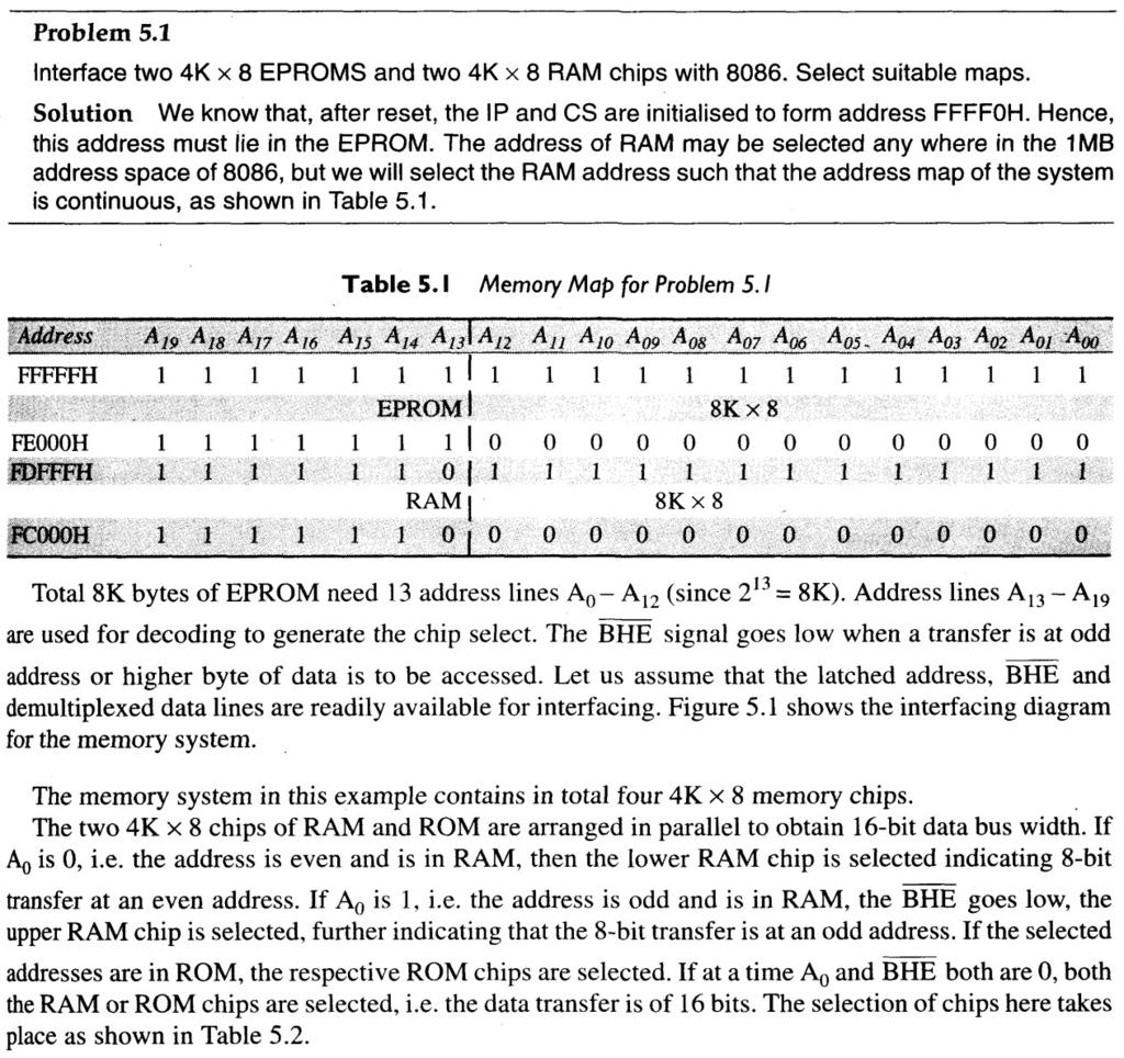
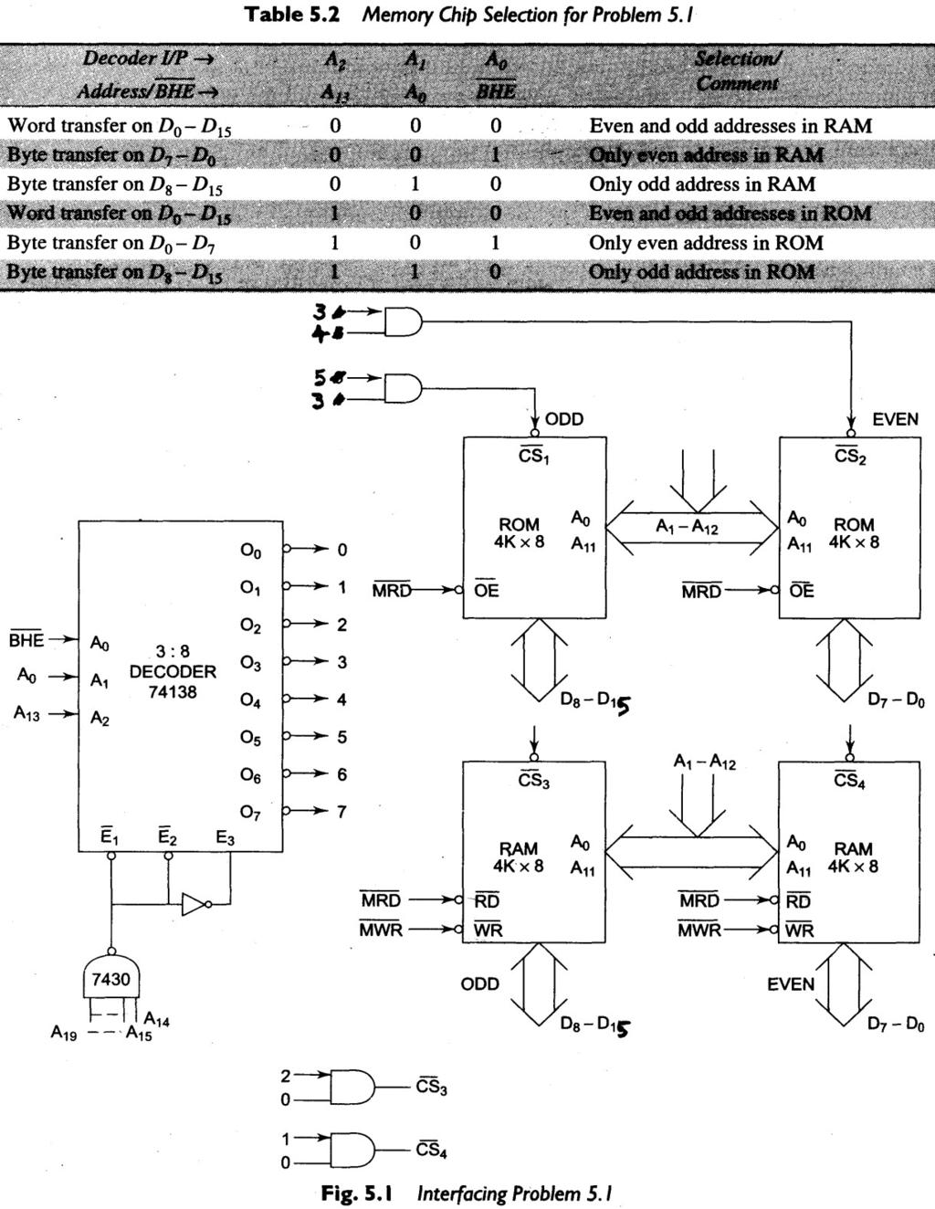
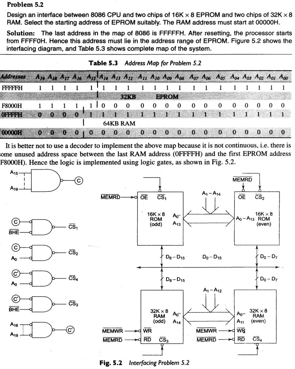
18 task both CS and OE must be active. A RAM contains one or two control inputs. They are R /W or RD and WR. If there is only one input R/W then it performs read operation when R/W pin is at logic 1. If it is at logic 0 it performs write operation. Note that this is possible only when CS is also active. Memory Interface using RAMS, EPROMS and EEPROMS: Semiconductor Memory Interfacing: Semiconductor memories are of two types, viz. RAM (Random Access Memory) and ROM (Read Only Memory). Static RAM Interfacing: The semiconductor RAMs are of broadly two types-static RAM and dynamic RAM. The semiconductor memories are organised as two dimensional arrays of memory locations. For example, 4K x 8 or 4K byte memory contains 4096 locations, where each location contains 8-bit data and only one of the 4096 locations can be selected at a time. Obviously, for addressing 4K bytes of memory, twelve address lines are required. In general, to address a memory location out of N memory locations, we will require at least n bits of address, i.e. n address lines where n = Log2 N. Thus if the microprocessor has n address lines, then it is able to address at the most N locations of memory, where 2n = N. However, if out of N locations only P memory locations are to be interfaced, then the least significant p address lines out of the available n lines can be directly connected from the microprocessor to the memory chip while the remaining (n-p) higher order address lines may be used for address decoding (as inputs to the chip selection logic). The memory address depends upon the hardware circuit used for decoding the chip select ( CS ). The output of the decoding circuit is connected with the CS pin of the memory chip. The general procedure of static memory interfacing with 8086 is briefly described as follows: 1. Arrange the available memory chips so as to obtain 16-bit data bus width. The upper 8-bit bank is called odd address memory bank and the lower 8-bit bank is called even address memory bank. 2. Connect available memory address lines of memory chips with those of the microprocessor and also connect the memory RD and WR inputs to the corresponding processor control signals. Connect the 16-bit data bus of the memory bank with that of the microprocessor The remaining address lines of the microprocessor, BHE and A0 are used for decoding the required chip select signals for the odd and even memory banks. CS of memory is derived from the O/P of the decoding circuit. As a good and efficient interfacing practice, the address map of the system should be continuous as far as possible, i.e. there should be no windows in the map. A memory location should have a single address corresponding to it, i.e. absolute decoding should be preferred, and minimum hardware should be used for decoding. In a number of cases, linear decoding may be used to minimize the required hardware. Let us now consider a few example problems on memory interfacing with 8086.
19
20
21
22 UNIT-IV 8255 PPI:
23 Features: 3 8-bit IO ports PA, PB, PC PA can be set for Modes 0, 1, 2. PB for 0,1 and PC for mode 0 and for BSR. Modes 1 and 2 are interrupt driven. PC has 2 4-bit parts: PC upper (PCU) and PC lower (PCL), each can be set independently for I or O. Each PC bit can be set/reset individually in BSR mode. PA and PCU are Group A (GA) and PB and PCL are Group B (GB) Address/data bus must be externally demux'd. TTL compatible. Improved dc driving capability The 8255A is a programmable peripheral interface (PPI) device designed for use in Intel microcomputer systems. Its function is that of a general purposes I/O component to Interface peripheral equipment to the microcomputer system bush. The functional configuration of the 8255A is programmed by the systems software so that normally no external logic is necessary to interface peripheral devices or structures. ARCHITECTURE OF 8255 PPI:
24 The port A lines are identified by symbols PA0-PA7 while the port C lines are identified as PC4-PC7 similarly. Group B contains an 8-bit port B, containing lines PB0- PB7 and a 4-bit port C with lower bits PC0-PC3. The port C upper and port C lower can be used in combination as an 8-bit port C. Both the port Cs is assigned the same address. Thus one may have either three 8-bit I/O ports or two 8-bit and two 4-bit I/O ports from All of these ports can function independently either as input or as output ports. This can be achieved by programming the bits of an internal register of 8255 called as control word register (CWR). The internal block diagram and the pin configuration of 8255 are shown in figs. The 8-bit data bus buffer is controlled by the read/write control logic. The read/write control logic manages all of the internal and external transfer of both data and control words. RD, WR, A1, A0 and RESET are the inputs, provided by the microprocessor to READ/WRITE control logic of The 8-bit, 3-state bidirectional buffer is used to interface the 8255 internal data bus with the external system data bus. This buffer receives or transmits data upon the execution of input or output instructions by the microprocessor. The control words or status information is also transferred through the buffer. Pin Diagram of 8255A The pin configuration of 8255 is shown in fig.
25 The port A lines are identified by symbols PA0-PA7 while the port C lines are Identified as PC4-PC7. Similarly, Group B contains an 8-bit port B, containing lines PB0-PB7 and a 4-bit port C with lower bits PC0- PC3. The port C upper and port C lower can be used in combination as an 8-bit port C. Both the port C is assigned the same address. Thus one may have either three 8-bit I/O ports or two 8-bit and two 4-bit ports from All of these ports can function independently either as input or as output ports. This can be achieved by programming the bits of an internal register of 8255 called as control word register (CWR). The 8-bit data bus buffer is controlled by the read/write control logic. The read/write control logic manages all of the internal and external transfers of both data and control words. RD,WR, A1, A0 and RESET are the inputs provided by the microprocessor to the READ/ WRITE control logic of The 8-bit, 3-state bidirectional buffer is used to interface the 8255 internal data bus with the external system data bus. This buffer receives or transmits data upon the execution of input or output instructions by the microprocessor. The control words or status information is also transferred through the buffer. The signal description of 8255 is briefly presented as follows: PA7-PA0: These are eight port A lines that acts as either latched output or buffered input lines depending upon the control word loaded into the control word register. PC7-PC4: Upper nibble of port C lines. They may act as either output latches or input buffers lines. This port also can be used for generation of handshake lines in mode1 or mode2. PC3-PC0: These are the lower port C lines; other details are the same as PC7PC4 lines. PB0-PB7: These are the eight port B lines which are used as latched output lines or buffered input lines in the same way as port A. RD: This is the input line driven by the microprocessor and should be low to indicate read operation to WR: This is an input line driven by the microprocessor. A low on this line indicates write operation. CS: This is a chip select line. If this line goes low, it enables the 8255 to respond to RD and WR signals, otherwise RD and WR signal are neglected. D0-D7: These are the data bus lines those carry data or control word to/from the microprocessor. RESET:Logic high on this line clears the control word register of All ports
26 are set as input ports by default after reset. A1-A0: These are the address input lines and are driven by the microprocessor. These lines A1-A0 with RD, WR and CS from the following operations for These address lines are used for addressing any one of the four registers, i.e. three ports and a control word register as given in table below. In case of 8086 systems, if the 8255 is to be interfaced with lower order data bus, the A0 and A1 pins of 8255 are connected with A1 and A2 respectively. Operational modes of 8255 There are two basic operational modes of 8255: Bit set/reset mode (BSR mode). Input/Output mode (I/O mode). The two modes are selected on the basis of the value present at the D 7 bit of the control word register. When D7 = 1, 8255 operates in I/O mode, and when D 7 = 0, it operates in the BSR mode. Bit set/reset (BSR) mode The Bit Set/Reset (BSR) mode is applicable to port C only. Each line of port C (PC 0 - PC7) can be set/reset by suitably loading the control word register. BSR mode and I/O mode are independent and selection of BSR mode does not affect the operation of other ports in I/O mode.

27 8255 BSR mode D7 bit is always 0 for BSR mode. Bits D6, D5 and D4 are don't care bits. Bits D3, D2 and D1 are used to select the pin of Port C. Bit D0 is used to set/reset the selected pin of Port C. Selection of port C pin is determined as follows: B B B Bit/pin of port C selected PC0 PC1 PC2 PC3 PC4 PC5 PC6 PC7 As an example, if it is needed that PC5 be set, then in the control word, 1. Since it is BSR mode, D7 = '0'. 2. Since D4, D5, D6 are not used, assume them to be '0'. 3. PC5 has to be selected, hence, D3 = '1', D2 = '0', D1 = '1'. 4. PC5 has to be set, hence, D0 = '1'. Thus, as per the above values, 0B (Hex) will be loaded into the Control Word Register (CWR). D 7 0 Input/Output mode D 6 0 D 5 0 D 4 0 D 3 1 D 2 0 D 1 1 D0 1

28 This mode is selected when D7 bit of the Control Word Register is 1. There are three I/O modes. 1. Mode 0 - Simple I/O 2. Mode 1 - Strobed I/O 3. Mode 2 - Strobed Bi-directional I/O Control Word Format I/O Control Word Format D0, D1, D3, D4 are assigned for port C lower, port B, port C upper and port A respectively. When these bits are 1, the corresponding port acts as an input port. For e.g., if D0 = D4 = 1, then lower port C and port A act as input ports. If these bits are 0, then the corresponding port acts as an output port. For e.g., if D 1 = D3 = 0, then port B and upper port C act as output ports. D2 is used for mode selection of Group B (port B and lower port C). When D 2 = 0, mode 0 is selected and when D2 = 1, mode 1 is selected. D5 & D6 are used for mode selection of Group A ( port A and upper port C). The selection is done as follows: D D5 0 1 X Mode As it is I/O mode, D7 = 1. For example, if port B and upper port C have to be initialized as input ports and lower port C and port A as output ports (all in mode 0): 1. Since it is an I/O mode, D7 = Mode selection bits, D2, D5, D6 are all 0 for mode 0 operation.
29 3. Port B and upper port C should operate as Input ports, hence, D1 = D3 = Port A and lower port C should operate as Output ports, hence, D4 = D0 = 0. Hence, for the desired operation, the control word register will have to be loaded with " " = 8A (hex). A) Mode 0 - simple I/O In this mode, the ports can be used for simple I/O operations without handshaking signals. Port A, port B provide simple I/O operation. The two halves of port C can be either used together as an additional 8-bit port, or they can be used as individual 4-bit ports. Since the two halves of port C are independent, they may be used such that one-half is initialized as an input port while the other half is initialized as an output port. The input/output features in mode 0 are as follows: 1. Output ports are latched. 2. Input ports are buffered, not latched. 3. Ports do not have handshake or interrupt capability. 4. With 4 ports, 16 different combinations of I/O are possible. Mode 0 input mode In the input mode, the 8255 gets data from the external peripheral ports and the CPU reads the received data via its data bus. The CPU first selects the 8255 chip by making CS low. Then it selects the desired port using A0 and A1 lines. The CPU then issues an RD signal to read the data from the external peripheral device via the system data bus. Mode 0 - output mode In the output mode, the CPU sends data to 8255 via system data bus and then the external peripheral ports receive this data via 8255 port. CPU first selects the 8255 chip by making CS low. It then selects the desired port using A0 and A1 lines. CPU then issues a WR signal to write data to the selected port via the system data bus. This data is then received by the external peripheral device connected to the selected port.
30 b) Mode 1: ( Strobed input/output mode ) In this mode the handshaking control the input and output action of the specified port. Port C lines PC0-PC2, provide strobe or handshake lines for port B. This group which includes port B and PC0-PC2 is called as group B for Strobed data input/output. Port C lines PC3-PC5 provides strobe lines for porta. This group including port A and PC3-PC5 from group A. Thus port C is utilized for generating handshake signals. The salient features of mode 1 are listed as follows: 1. Two groups group A and group B are available for strobed data transfer. 2. Each group contains one 8-bit data I/O port and one 4-bit control/data port. 3. The 8-bit data port can be either used as input and output port. The inputs andoutputs both are latched. 4. Out of 8-bit port C, PC0-PC2 are used to generate control signals for port B andpc3-pc5 are used to generate control signals for port A. the lines PC6, PC7 may be used as independent data lines. The control signals for both the groups in input and output modes are explained as follows: Input control signal defnitions (mode 1): STB (Strobe input) If this lines falls to logic low level, the data available at 8-bit input port is loaded into input latches. IBF (Input buffer full) If this signal rises to logic 1, it indicates that data has been loaded into latches, i.e. it works as an acknowledgement. IBF is set by a low on STB and is reset by the rising edge of RD input. INTR (Interrupt request) This active high output signal can be used to interrupt the CPU whenever an input device requests the service. INTR is set by a high STB pin and a high at IBF pin. INTE is an internal flag that can be controlled by the bit set/reset mode of either PC4 (INTEA) or PC2 (INTEB) as shown in fig. INTR is reset by a falling edge of RD input. Thus an external input device can be request the service of the processor by putting the data on the bus and sending the strobe signal. Output control signal definitions (mode 1): OBF (Output buffer full) This status signal, whenever falls to low, indicates that CPU has written data to the specified output port. The OBF flipflop will beset by a rising edge of WR signal and reset by a low going edge at the ACK input. ACK (Acknowledge input) ACK signal acts as an acknowledgement to be given by an output device. ACK signal, whenever low, informs the CPU that the data transferred by the CPU to the output device through the port is received by the output device. INTR (Interrupt request) Thus an output signal that can be used to interrupt the CPU when an output device acknowledges the data received from the CPU.INTR is set when ACK, OBF and INTE are 1. It is reset by a
31
32 c) Mode 2 (Strobed bidirectional I/O): This mode of operation of 8255 is alsocalled as strobed bidirectional I/O. This mode of operation provides 8255 with additional features for communicating with a peripheral device on an 8-bit databus. Handshaking signals are provided to maintain proper data flow andsynchronization between the data transmitter and receiver. The interruptgeneration and other functions are similar to mode 1.
33 In this mode, 8255 is a bidirectional 8-bit port with handshake signals. The Rd and WR signals decide whether the 8255 is going to operate as an input port or output port. The Salient features of Mode 2 of 8255 are listed as follows: 1. The single 8-bit port in group A is available. 2. The 8-bit port is bidirectional and additionally a 5-bit control port is available. 3. Three I/O lines are available at port C.( PC2 PC0 ) 4. Inputs and outputs are both latched. 5. The 5-bit control port C (PC3-PC7) is used for accepting handshake signals for the 8-bit data transfer on port A. generating / Control signal definitions in mode 2: INTR (Interrupt request) As in mode 1, this control signal is active high and is used to interrupt the microprocessor to ask for transfer of the next data byte to/from it. This signal is used for input (read) as well as output (write) operations. Control Signals for Output operations: OBF (Output buffer full) This signal, when falls to low level, indicates that the CPU has written data to port A. ACK (Acknowledge) This control input, when falls to logic low level, Acknowledges that the previous data byte is received by the destination and next byte may be sent by the processor. This signal enables the internal tri state buffers to send the next data byte on port A. INTE1 ( A flag associated with OBF ) This can be controlled by bit t/reset mode with PC6. Control signals for input operations: STB (Strobe input)a low on this line is used to strobe in the data into the input Latches of IBF (Input buffer full) when the data is loaded into input buffer, this signal rises to logic 1. This can be used as an acknowledge that the data has been received by the receiver. The waveforms in fig show the operation in Mode 2 for output as well as input port. Note: WR must occur before ACK and STB must be activated before RD.
34
35 8253(PROGRAMMABLE INTERVAL TIMER/COUNTER): The Intel 8253 and 8254 are Programmable Interval Timers (PITs), which perform timing and counting functions using three 16-bit counters. [1] They were primarily designed for the Intel 8080/8085processors, but later used in x86-systems. They (or an equivalent circuit embedded in a larger chip) are found in all IBM PC compatibles. The Intel 82c54 variant handles up to 10 MHz clock signals. The timer has three counters, called channels. Each channel can be programmed to operate in one of six modes. Once programmed, the channels can perform their tasks independently. The timer is usually assigned to IRQ-0 (highest priority hardware interrupt) because of the critical function it performs and because so many devices depend on it. Counters There are 3 counters (or timers), which are labeled as "Counter 0", "Counter 1" and "Counter 2".[3] Each counter has 2 input pins "CLK" (clock input) and "GATE" and 1-pin, "OUT", for data output. The 3 counters are 16-bit down counters independent of each other, and can be easily read by the CPU. In the original IBM PCs, the first counter (selected by setting A1=A0=0, see Control Word Register below) is used to generate a timekeeping interrupt. The second counter (A1=0, A0=1) is used to trigger the refresh of DRAM memory. The last counter (A1=1, A0=0) is used to generate tones via the PC speaker. Besides the counters, a typical Intel 8253 microchip also contains the following components: Data/Bus Buffer This block contains the logic to buffer the data bus to / from the microprocessor, and to the internal registers. It has 8 input pins, usually labelled as D7..D0, where D7 is the MSB. Read/Write Logic The Read/Write Logic block has 5 pins, which are listed below. Notice that "/X" denotes an active low signal. /RD: read signal /WR: write signal /CS: chip select signal A0, A1: address lines
36 Operation mode of the PIT is changed by setting the above hardware signals. For example, to write to the Control Word Register, one needs to set /CS=0, /RD=1, /WR=0, A1=A0=1. Control Word Register This register contains the programmed information which will be sent (by the to the device. It defines how the PIT logically works. Each access to these ports takes about 1 µs. To initialize the counters, the microprocessor must write a control word (CW) in this register. This can be done by setting proper values for the pins of the Read/Write Logic block and then by sending the control word to the Data/Bus Buffer block. The control word register contains 8 bits, labeled D7..D0 (D7 is the MSB). When setting the PIT, the microprocessor first sends a control message, then a count message to the PIT. The counting process will start after the PIT has received these messages, and, in some cases, if it detects the rising edge from the GATE input signal. On PCs the address for timer0 (chip) is at port 40h..43h like described and the second timer1 (chip) is at 50h..53h.

: Interrupt on Terminal Count Mode 0 is used for the generation of accurate time delay under software control.")
37 O peration Modes The D3, D2, and D1 bits of the Control Word set the operating mode of the timer. There are 6 modes in total; for modes 2 and 3, the D3 bit is ignored, so the missing modes 6 and 7 are aliases for modes 2 and 3. Notice that, for modes 0, 2, 3 and 4, GATE must be set to HIGH to enable counting. For mode 5, the rising edge of GATE starts the count. For details on each mode, see the reference links. Mode 0 (000): Interrupt on Terminal Count Mode 0 is used for the generation of accurate time delay under software control. In this mode, the counter will start counting from the initial COUNT value loaded into it, down to 0. Counting rate is equal to the input clock frequency. The OUT pin is set low after the Control Word is written, and counting starts one clock cycle after the COUNT programmed. OUT remains low until the counter reaches 0, at which point OUT will be set high until the counter is reloaded or the Control Word is written. The Gate signal should remain active high for normal counting. If Gate goes low, counting gets terminated and current count is latched till Gate pulse goes high again. The first byte of the new count when loaded in the count register, stops the previous count. Mode 1 (001): Programmable One Shot In this mode 8253 can be used as Monostable Multivibrator. GATE input is used as trigger input. OUT will be initially high. OUT will go low on the Clock pulse following a trigger to begin the one-shot pulse, and will remain low until the Counter reaches zero. OUT will then go high and remain high until the CLK pulse after the next trigger.
38 After writing the Control Word and initial count, the Counter is armed. A trigger results in loading the Counter and setting OUT low on the next CLK pulse, thus starting the one-shot pulse. An initial count of N will result in a one-shot pulse N CLK cycles in duration. The one-shot is retriggerable, hence OUT will remain low for N CLK pulses after any trigger. The one-shot pulse can be repeated without rewriting the same count into the counter. GATE has no effect on OUT. If a new count is written to the Counter during a oneshot pulse, the current one-shot is not affected unless the counter is retriggered. In that case, the Counter is loaded with the new count and the oneshot pulse continues until the new count expires. Mode 2 (X10): Rate Generator In this mode, the device acts as a divide-by-n counter, which is commonly used to generate a real-time clock interrupt. Like other modes, counting process will start the next clock cycle after COUNT is sent. OUT will then remain high until the counter reaches 1, and will go low for one clock pulse. OUT will then go high again, and the whole process repeats itself. The time between the high pulses depends on the preset count in the counter's register, and is calculated using the following formula: Note that the values in the COUNT register range from to 1; the register never reaches zero. Mode 3 (X11): Square Wave Generator This mode is similar to mode 2. However, the duration of the high and low clock pulses of the output will be different from mode 2. Suppose N is the number loaded into the counter (the COUNT message), the output will be high for N / 2 counts, and low for N /2 counts, if N is even. high for N + 1 / 2counts, and low for N ½ counts, if N is odd. Mode 4 (100): Software Triggered Strobe After Control Word and COUNT is loaded, the output will remain high until the counter reaches zero. The counter will then generate a low pulse for 1 clock cycle (a strobe) after that the output will become high again. Mode 5 (101): Hardware Triggered Strobe This mode is similar to mode 4. However, the counting process is triggered by the GATE input.

39 After receiving the Control Word and COUNT, the output will be set high. Once the device detects a rising edge on the GATE input, it will start counting. When the counter reaches 0, the output will go low for one clock cycle after that it will become high again, to repeat the cycle on the next rising edge of GATE (PIC): The processor 8085 had five hardware interrupt pins. Out of these five interrupt pins, four pins were allotted fixed vector addresses but the pin INTR was not allotted any vector address, rather an external device was supposed to hand over the type of the interrupt, i.e. (Type 0 to 7 for RST0 to RST7), to the microprocessor. The microprocessor then gets this type and derives the interrupt vector address from that. Consider an application, where a number of I/O devices connected with a CPU desire to transfer data using interrupt driven data transfer mode. In these types of applications, more number of interrupt pins are required than available in a typical microprocessor. Moreover, in these multiple interrupt systems, the processor will have to take care of the priorities for the interrupts, simultaneously occur ring at the interrupt request pins. To overcome all these difficulties, we require a programmable interrupt controller which is able to handle a number of interrupts at a time. This controller takes care of a number of simultaneously appearing interrupt requests along with their types and priorities. This will relieve the processor from all these tasks. The programmable interrupt controller 8259A from Intel is one such device. The predecessor 8259 was designed to operate only with 8-bit processors like A modified version, 8259A was later introduced that is compatible with 8-bit as well as 16-bit processors.
40 Architecture and Signal Descriptions of 8259A: The architectural block diagram of 8259A is shown in Fig. The functional explanation of each block is given in the following text in brief. Interrupt Request Register (IRR) The interrupts at IRQ input lines are handled by Interrupt Request Register internally. IRR stores all the interrupt requests in it in order to serve them one by one on the priority basis. In-Service Register (ISR) This stores all the interrupt requests those are being served, i.e ISR keeps a track of the requests being served. Priority Resolver This unit determines the priorities of the interrupt requests appearing simultaneously. The highest priority is selected and stored into the corresponding bit of ISR during INTA pulse. The IR0 has the highest priority while the IR7 has the lowest one, normally in fixed priority mode. The priorities however may be altered by programming the 8259A in rotating priority mode. Interrupt Mask Register (IMR) This register stores the bits required to mask the interrupt puts. IMR operates on IRR at the direction of the Priority Resolver. Interrupt Control Logic This block manages the interrupt and interrupt acknowledge sigd8ls to be sent to the CPU for serving one of the eight interrupt requests. This also accepts interrupt acknowledge (INTA) signal from CPU that causes the 8259A to release vector address on to the data bus. Data Bus Buffer This tristate bidirectional buffer interfaces internal 8259A bus to the microprocessor system data bus. Control words, status and vector information pass through buffer during read or write operations. Read write Control Logic This circuit accepts and decodes commands from the CPU. This also allows the status of the 8259A to be transferred on to the data bus.

41 Cascade Buffer/Comparator This block stores and compares the ID's of all the 8259As used in the system. The three I/O pins CAS0-2 are outputs when the 8259A is used as a master. The same pins act as inputs when the 8259A is in slave mode. The 8259A in master mode sends the ID of the interrupting slave device on these lines. The slave thus selected, will send its pre programmed vector address on the data bus during the next INTA pulse. Figure 1.2 shows the pin configuration of 8259A, followed by their functional description of each of the signals in brief. CS : This is an active-low chip select signal for enabling RD* and WR* operations of 8259A.INTA* function is independent of CS*. WR* : This pin is an active-low write enable input to 8259A. This enables it to accept command words from CPU. RD* :This is an active-low read enable input to 8259A. A low on this line enables 8259A to release status onto the data bus of CPU. D7-D0 These pins form a bidirectional data bus that carries 8-bit data either to control word or from status word registers. This also carries interrupt vector information.
42 CASo-CAS2: Cascade Lines A single 8259A provides eight vectored interrupts. If more interrupts are required, the 8259A is used in cascade mode. In cascade mode, a master 8259A along with eight slaves 8259A can provide up to 64 vectored interrupt lines. These three lines act as select lines for addressing the slaves 8259A. PS*/EN*: This pin is a dual purpose pin. When the chip is used in buffered mode, it can be used as buffer enable to control buffer transreceivers. If this is not used in buffered mode then the pin is used as input to designate whether the chip is used as a master (SP = 1) or a slave (EN = 0). INT: This pin goes high whenever a valid interrupt request is asserted. This is used to interrupt the CPU and is connected to the interrupt input of CPU. IR0-IR7 (1nterrupt requests): These pins act as inputs to accept interrupt requests to the CPU. In edge triggerred mode, an interrupt service is requested by raising an IR pin from a low to a high state and holding it high until it is acknowledged, and just by latching it to high level, if used in level triggered mode. INTA* (Interrupt acknowledge): This pin is an input used to strobe-in 8259A interrupt vector data on to the data bus. In conjunction with CS, WR, and RD pins, this selects the different operations like, writing command words, reading status word, etc. The device 8259A can be interfaced with any CPU using either polling or interrupt. In polling, the CPU keeps on checking each peripheral device in sequence to ascertain if it requires any service from the CPU. If any such service request is noticed, the CPU serves the request and then goes on to the next device in sequence. After all the peripheral devices are scanned as above the CPU again starts from the first device. This type of system operation results in the reduction of processing speed because most of the CPU time is consumed in polling the peripheral devices. In the interrupt driven method, the CPU performs the main processing task till it is interrupted by a service requesting peripheral device. The net processing speed of these type of systems is high because the CPU serves the peripheral only if it receives the interrupt request. If more than one interrupt requests are received at a time, all the requesting peripherals are served one by one on priority basis. This method of interfacing may require additional hardware if number of peripherals to be interfaced is more than the interrupt pins available with the CPU. Interrupt Sequence in an 8086 System: The interrupt sequence in an A system is described as follows: 1. One or more IR lines are raised high that set corresponding IRR bits A resolves priority and sends an INT signal to CPU. 3. The CPU acknowledges with INTA pulse.
43 4. Upon receiving an INTA signal from the CPU, the highest priority ISR bit is set and the corresponding IRR bit is reset. The 8259A does not drive data bus during this period. 5. The 8086 will initiate a second INTA pulse. During this period 8259A releases an 8-bit pointer on to data bus from where it is read by the CPU. 6. This completes the interrupt cycle. The ISR bit is reset at the end of the second INTA pulse if automatic end of interrupt (AEOI) mode is programmed. Otherwise ISR bit remains set until an appropriate EOI command is issued at the end of interrupt subroutine.
44 Command Words of 8259A The command words of 8259A are classified in two groups, viz. initialization command words (ICWs) and operation command words (OCWs)Initialization Command Words (ICWs) Before it starts functioning, the 8259A must be initialized by writing two to four command words into the respective command word registers. These are called as initialization command words (ICWs). If A0 = 0 and D4 = 1, the control word is recognized as ICW1 It contains the control bits for edge/level triggered mode, single/cascade mode, call address interval and whether ICW4 is required or not, etc. If A0 = 1, the control word is recognized as ICW2. The ICW2 stores details regarding interrupt vector addresses. The initialisation sequence of 8259A is described in from of a flow chart in Fig The bit functions of the ICW1 and ICW2 are self explanatory as shown in Fig Once ICW1 is loaded, the following initialization procedure is carried out internally. (a) The edge sense circuit is reset, i.e. by default 8259A interrupts are edge sensitive. (b) IMR is cleared. (c) IR7 input is assigned the lowest priority. (d) Slave mode address is set to 7. (e) Special mask mode is cleared and status read is set to IRR. (f) If IC4 = 0, all the functions of ICW4 are set to zero. Master/slave bit in ICW4 is used in the buffered mode only.
45 In an 8085 based system, A15 A8 of the interrupt vector address are the respective bits of ICW2. In 8086/88 based system A15 A11 of the interrupt vector address are inserted in place of T7 - T3 respectively and the remaining three bits (A8, A9 and A10) are selected depending upon the interrupt level, i.e. from 000 to 111 for IR0 to IR7. ICW1 and ICW2 are compulsory command words in initialization sequence of 8259A as is evident from Fig. 1.3, while ICW3 and ICW4 are optional. The ICW3 is read only when there are more than one 8259As in the system, i.e. cascading is used (SNGL = 0). The SNGL bit in ICW1 indicates whether the 8259A is in cascade mode or not. The ICW3 loads an 8-bit slave register. Its detailed functions are as follows.
46 In master mode [i.e. SP = 1 or in buffer mode M/S = 1 in ICW4], the 8-bit slave register will be set bit-wise to '1' for each slave in the system, as shown in Fig The requesting slave will then release the second byte of a CALL sequence. In slave mode [i.e.sp=0 or if BUF=1 and M/S=0 in ICW4] bits D2 to D0 identify the slave, i.e 000 to 111 for slave 1 to slave 8. The slave compares the cascade inputs with these bits and if they are equal, the second byte if the CALL sequence is released by it on the data bus.
47
48 ICW4 The use of this command word depends on the IC4 bit of ICW1. If IC4= 1, ICW4 is used, otherwise it is neglected. The bit functions of ICW4 are described as follows: SFNM Special fully nested mode is selected, if SFNM = 1. BUF If BUF = 1, the buffered mode is selected. In the buffered mode,sp/en acts as enable output and the master/slave is determined using the M/S bit of ICW4. M/S If M/S = 1, 8259A is a master. If M/S = 0, 8259A is a slave. If BUF =0, M/S is to be neglected. AEOI If AEOI = 1, the automatic end of interrupt mode is selected. μpm If the μpm bit is 0, the Mcs-85 system operation is selected and if/μpm =1, 8086/88 operation is selected. Operation Command Words Once 8259A is initialized using the previously discussed command words for initialisation, it is ready for its normal function, i.e. for accepting the interrupts but 8259A has its own ways of handling the received interrupts called as modes of operation. These modes of operations can be selected by programming, i.e. writing three internal registers called as operation command word registers. The data written into them (bit pattern) is called as operation command words. In the three operation command words OCWl,OCW2 and OCW3 every bit corresponds to some operational feature of the mode selected, except for a few bits those are either '1' or '0'. The three operation command words are shown in Fig. 1.7 (a), (b) and (c) with the bit selection details. OCW1 is used to mask the unwanted interrupt requests. If the mask bit is '1', the corresponding interrupt request is masked, and if it is '0', the request is enabled. In OCW2 the three bits, viz. R, SL and EOI control the end of interrupt, the rotate mode and their combinations as shown in Fig. 1.7 (b), The three bits L2, L1 and L0 in OCW2 determine the interrupt level to be selected for operation, if the SL bit is active, i.e. '1'. The details of OCW2 are shown in Fig. 1.7(b). In operation command word 3 (OCW3), if the ESMM bit, i.e. enable special mask mode bit is
49 set to '1', the SMM bit is enabled to select or mask the special mask mode. When ESMM bit is '0', the SMM bit is neglected. If the SMM bit, i.e.special mask mode bit is '1', the 8259A will enter special mask mode provided ESMM = 1. If ESMM = 1 and SMM = 0, the 8259A will return to the normal mask mode. The details of bits of OCW3 are given in Fig. 1.7 (c) along with their bit definitions.
50
51 SERIAL COMMUNICATION USING is a Universal Synchronous and Asynchronous Receiver and Transmitter compatible with Intel s processors. This chip converts the parallel data into a serial stream of bits suitable for serial transmission. It is also able to receive a serial stream of bits and convert it into parallel data bytes to be read by a microprocessor. Basic Modes of data transmission a) b) c) Half Duplex Simplex Duplex a) Simplex mode Data is transmitted only in one direction over a single communication Channel. For example, the processor may transmit data for a CRT display unit in this mode. b) Duplex Mode In duplex mode, data may be transferred between two transreceivers in both directions Simultaneously. c) Half Duplex mode In this mode, data transmission may take place in either direction, but at a time data may be transmitted only in one direction. A computer may communicate with a terminal in this mode. It is not possible to transmit data from the computer to the terminal and terminal to computer simultaneously. ARCHITECTURE OF 8251 USART:
52 The data buffer interfaces the internal bus of the circuit with the system bus. The read / write control logic controls the operation of the peripheral depending upon theoperations initiated by the CPU. C / decides whether the address on internal data bus is control address / data address. The modem control unit handles the modem handshake signals to coordinate the communication between modem and USART. The transmit control unit transmits the data byte received by the data buffer from the CPU for serial communication. The transmission rate is controlled by the input frequency. Transmit control unit also derives two transmitter status signals namely TXRDY and TXEMPTY which may be used by the CPU for handshaking. The transmit buffer is a parallel to serial converter that receives a parallel byte for conversion into a serial signal for further transmission. The receive control unit decides the receiver frequency as controlled by therxc input frequency. The receive control unit generates a receiver ready (RXRDY) signal that may be used by the CPU for handshaking. This unit also detects a break in the data string while the 8251 is in asynchronous mode. Signal Description of 8251:
53 Operating Modes of Asynchronousmode 2. Synchronous mode Asynchronous Mode (Transmission) When a data character is sent to 8251A by the CPU, it adds start bits prior to the serial data bits, followed by optional parity bit and stop bits using the asynchronous mode instruction control word format. This sequence is then transmitted using TXD output pin on the falling edge of TXC. Asynchronous Mode (Receive) A falling edge on RXD input line marks a start bit. The receiver requires only one stop bit to mark end of the data bit string, regardless of the stop bit programmed at the transmitting end. The 8-bit character is then loaded into the into parallel I/O buffer of 8251.
54 RXRDY pin is raised high to indicate to the CPU that a character is ready for it. If the previous character has not been read by the CPU, the new character replaces it, and the overrun flag is set indicating that the previous character is lost. Mode instruction format for Asynchronous mode Asynchronous Mode Transmit and Receive Formats Fig. 8.4 Asynchronous Mode Transmit and Receive Formats
55 Synchronous mode Synchronous Mode Instruction Format Synchronous Mode (Transmission) The TXD output is high until the CPU sends a character to 8251 which usually is a SYNC character. When line goes low, the first character is serially transmitted out. Characters are shifted out on the falling edge of.data is shifted out at the same rate as, over TXD output line. If the CPU buffer becomes empty, the SYNC character or characters are inserted in the data stream over TXD output. Synchronous Mode (Receiver) In this mode, the character synchronization can be achieved internally or externally. The data on RXD pin is sampled on rising edge of the. The content of the receiver buffer is compared with the first SYNC character at every edge until it matches. If 8251 is programmed for two SYNC characters, the subsequent received character is also checked. When the characters match, the hunting stops. The SYNDET pin set high and is reset automatically by a status read operation. In the external SYNC mode, the synchronization is achieved by applying a high level on the SYNDET input pin that forces 8251 out of HUNT mode. The high level can be removed after one cycle. The parity and overrun error both are checked in the same way as in asynchronous mode.
56 Synchronous mode Transmit and Receive data format Command Instruction Defnition The command instruction controls the actual operations of the selected format like enable transmit/receive, error reset and modem control. A reset operation returns 8251 back to mode instruction format.
57 Status Read Defnition This definition is used by the CPU to read the status of the active 8251 to confirm if any error condition or other conditions like the requirement of processor service has been detected during the operation.

58 Block Diagram of Internal Registers CAR The current address register holds a 16-bit memory address used for the DMA transfer. each channel register for this purpose. When a byte of data is transferred during a DMA operation, CAR is either incremented or decremented. depending on how it is programmed has its own current address CWCR The current word count register programs a channel for the number of bytes to transferred during a DMA action. CR The command register programs the operation of the 8237 DMA controller. The register uses bit position 0 to select the memory-to-memory DMA transfer mode.
 and base word count (BWC) registers are used when auto-initialization is selected for a channel.")
59 1. Memory-to-memory DMA transfers use DMA channel 2. DMA channel 0 to hold the source address 3. DMA channel 1 holds the destination address BA and BWC The base address (BA) and base word count (BWC) registers are used when auto-initialization is selected for a channel. In auto-initialization mode, these registers are used to reload the CAR and CWCR after the DMA action is completed. MR The mode register programs the mode of operation for a channel. Each channel has its own mode register as selected by bit positions 1 and Remaining bits of the mode register select operation, auto-initialization, increment/decrement, and mode for the channel
Features: 3 8-bit IO ports PA, PB, PC. PA can be set for Modes 0, 1, 2. PB for 0,1 and PC for mode 0 and for BSR. Modes 1 and 2 are interrupt driven.
 Features: 3 8-bit IO ports PA, PB, PC PA can be set for Modes, 1, 2. PB for,1 and PC for mode and for BSR. Modes 1 and 2 are interrupt driven. PC has 2 4-bit parts: PC upper (PCU) and PC lower (PCL), each
These three counters can be programmed for either binary or BCD count.
 S5 KTU 1 PROGRAMMABLE TIMER 8254/8253 The Intel 8253 and 8254 are Programmable Interval Timers (PTIs) designed for microprocessors to perform timing and counting functions using three 16-bit registers.
PIO 8255 (cont..) M Krishna kumar MAM/M3/LU9e/V1/2004 1
 M Krishna kumar MAM/M3/LU9e/V1/2004 1") PIO 8255 (cont..) The parallel input-output port chip 8255 is also called as programmable peripheral input-output port. The Intel s 8255 is designed for use with Intel s 8-bit, 16-bit and higher capability
PIO 8255 (cont..) The parallel input-output port chip 8255 is also called as programmable peripheral input-output port. The Intel s 8255 is designed for use with Intel s 8-bit, 16-bit and higher capability
8086 Interrupts and Interrupt Responses:
 UNIT-III PART -A INTERRUPTS AND PROGRAMMABLE INTERRUPT CONTROLLERS Contents at a glance: 8086 Interrupts and Interrupt Responses Introduction to DOS and BIOS interrupts 8259A Priority Interrupt Controller
Topics. Interfacing chips
 8086 Interfacing ICs 2 Topics Interfacing chips Programmable Communication Interface PCI (8251) Programmable Interval Timer (8253) Programmable Peripheral Interfacing - PPI (8255) Programmable DMA controller
8255 Programmable Peripheral Interface Architecture MCT/UNIT III/NARASIMHARAJ/LECTURE NOTES /IV MECH A
 8255 Programmable Peripheral Interface Architecture 8255 PPI Architecture The parallel input-output port chip 8255 is also called as programmable peripheral input- output port. The Intel s 8255 is designed
9. PERIPHERAL CHIPS 9a
 9. PERIPHERAL CHIPS 9a 8255: Programmable Peripheral Interface. Draw the pin diagram of PPI 8255. Ans. The pin diagram of 8255 is shown in Fig. 9a. PA 3 4 PA 4 PA2 2 39 PA 5 PA 3 38 PA 6 PA 4 37 PA7 RD
UNIT - II PERIPHERAL INTERFACING WITH 8085
 UNIT - II PERIPHERAL INTERFACING WITH 8085 Peripheral Interfacing is considered to be a main part of Microprocessor, as it is the only way to interact with the external world. The interfacing happens with
8254 is a programmable interval timer. Which is widely used in clock driven digital circuits. with out timer there will not be proper synchronization
 8254 is a programmable interval timer. Which is widely used in clock driven digital circuits. with out timer there will not be proper synchronization between two devices. So it is very useful chip. The
EC2304-MICROPROCESSOR AND MICROCONROLLERS 2 marks questions and answers UNIT-I
 EC2304-MICROPROCESSOR AND MICROCONROLLERS 2 marks questions and answers 1. Define microprocessors? UNIT-I A semiconductor device(integrated circuit) manufactured by using the LSI technique. It includes
Module 3. Embedded Systems I/O. Version 2 EE IIT, Kharagpur 1
 Module 3 Embedded Systems I/O Version 2 EE IIT, Kharagpur 1 Lesson 15 Interrupts Version 2 EE IIT, Kharagpur 2 Instructional Objectives After going through this lesson the student would learn Interrupts
Address connections Data connections Selection connections
 Interface (cont..) We have four common types of memory: Read only memory ( ROM ) Flash memory ( EEPROM ) Static Random access memory ( SARAM ) Dynamic Random access memory ( DRAM ). Pin connections common
CHAPTER: 3 PROGRAMMABLE PERIPHERAL INTERFACE & ELECTROMECHANICAL DEVICES INTERFACING
 CHAPTER: 3 1 PROGRAMMABLE PERIPHERAL INTERFACE & ELECTROMECHANICAL DEVICES INTERFACING Introduction to 8255 PPI 2 The Intel 8255A is a high-performance, general purpose programmable I/O device is designed
Northern India Engineering College, Delhi (GGSIP University) PAPER I
 PAPER I") PAPER I Q1.Explain IVT? ANS. interrupt vector table is a memory space for storing starting addresses of all the interrupt service routine. It stores CS:IP PAIR corresponding to each ISR. An interrupt vector
PAPER I Q1.Explain IVT? ANS. interrupt vector table is a memory space for storing starting addresses of all the interrupt service routine. It stores CS:IP PAIR corresponding to each ISR. An interrupt vector
2. List the five interrupt pins available in INTR, TRAP, RST 7.5, RST 6.5, RST 5.5.
 DHANALAKSHMI COLLEGE OF ENGINEERING DEPARTMENT OF ELECTRICAL AND ELECTRONICS ENGINEERING EE6502- MICROPROCESSORS AND MICROCONTROLLERS UNIT I: 8085 PROCESSOR PART A 1. What is the need for ALE signal in
To Interface The 8085 Microprocessor
 To Interface The 8085 Microprocessor A microprocessor has to be interfaced with various peripherals to perform various functions. Let's discuss about the Interfacing techniques in detail. Introduction
General Purpose Programmable Peripheral Devices. Assistant Professor, EC Dept., Sankalchand Patel College of Engg.,Visnagar
 Chapter 15 General Purpose Programmable Peripheral Devices by Rahul Patel, Assistant Professor, EC Dept., Sankalchand Patel College of Engg.,Visnagar Microprocessor & Interfacing (140701) Rahul Patel 1
Week 7. Input/Output Interface Circuits and LSI Peripheral Devices
 Week 7 Input/Output Interface Circuits and LSI Peripheral Devices Core and Special Purpose I/O Interfaces Special purpose I/O interfaces display parallel printer interface serial communication interface
1 MALP ( ) Unit-1. (1) Draw and explain the internal architecture of 8085.
 Unit-1. (1) Draw and explain the internal architecture of 8085.") (1) Draw and explain the internal architecture of 8085. The architecture of 8085 Microprocessor is shown in figure given below. The internal architecture of 8085 includes following section ALU-Arithmetic
(1) Draw and explain the internal architecture of 8085. The architecture of 8085 Microprocessor is shown in figure given below. The internal architecture of 8085 includes following section ALU-Arithmetic
Lecture Note On Microprocessor and Microcontroller Theory and Applications
 Lecture Note On Microprocessor and Microcontroller Theory and Applications MODULE: 1 1. INTRODUCTION TO MICROPROCESSOR AND MICROCOMPUTER ARCHITECTURE: A microprocessor is a programmable electronics chip
Control Unit: The control unit provides the necessary timing and control Microprocessor resembles a CPU exactly.
 Unit I 8085 and 8086 PROCESSOR Introduction to microprocessor A microprocessor is a clock-driven semiconductor device consisting of electronic logic circuits manufactured by using either a large-scale
UNIT-IV. The semiconductor memories are organized as two-dimensional arrays of memory locations.
 UNIT-IV MEMORY INTERFACING WITH 8086: The semi conductor memories are of two types: Static RAM Dynamic RAM The semiconductor memories are organized as two-dimensional arrays of memory locations. For Ex:
Chapter 8 Summary: The 8086 Microprocessor and its Memory and Input/Output Interface
 Chapter 8 Summary: The 8086 Microprocessor and its Memory and Input/Output Interface Figure 1-5 Intel Corporation s 8086 Microprocessor. The 8086, announced in 1978, was the first 16-bit microprocessor
The Purpose of Interrupt
 Interrupts 3 Introduction In this chapter, the coverage of basic I/O and programmable peripheral interfaces is expanded by examining a technique called interrupt-processed I/O. An interrupt is a hardware-initiated
1. INTRODUCTION TO MICROPROCESSOR AND MICROCOMPUTER ARCHITECTURE:
 1. INTRODUCTION TO MICROPROCESSOR AND MICROCOMPUTER ARCHITECTURE: A microprocessor is a programmable electronics chip that has computing and decision making capabilities similar to central processing unit
S.R.M. INSTITUTE OF SCIENCE & TECHNOLOGY SCHOOL OF ELECTRONICS & COMMUNICATION ENGINEERING
 S.R.M. INSTITUTE OF SCIENCE & TECHNOLOGY SCHOOL OF ELECTRONICS & COMMUNICATION ENGINEERING QUESTION BANK Subject Code : EC307 Subject Name : Microprocessor and Interfacing Year & Sem : III Year, V Sem
MAHALAKSHMI ENGINEERING COLLEGE TIRUCHIRAPALLI UNIT IV I/O INTERFACING PART A (2 Marks)
") MAHALAKSHMI ENGINEERING COLLEGE TIRUCHIRAPALLI-621213. UNIT IV I/O INTERFACING PART A (2 Marks) 1. Name the three modes used by the DMA processor to transfer data? [NOV/DEC 2006] Signal transfer mode (cycling
MAHALAKSHMI ENGINEERING COLLEGE TIRUCHIRAPALLI-621213. UNIT IV I/O INTERFACING PART A (2 Marks) 1. Name the three modes used by the DMA processor to transfer data? [NOV/DEC 2006] Signal transfer mode (cycling
INTERFACING INTERFACING. Richa Upadhyay Prabhu. NMIMS s MPSTME February 25, 2016
 INTERFACING Richa Upadhyay Prabhu NMIMS s MPSTME richa.upadhyay@nmims.edu February 25, 2016 8255: Programmable Peripheral Interface or Programmable Input output Device Introduction METHODS OF DATA TRANSFER
MP Assignment III. 1. An 8255A installed in a system has system base address E0D0H.
 MP Assignment III 1. An 8255A installed in a system has system base address E0D0H. i) Calculate the system addresses for the three ports and control register for this 8255A. System base address = E0D0H
MICROPROCESSOR AND MICROCONTROLLER BASED SYSTEMS
 MICROPROCESSOR AND MICROCONTROLLER BASED SYSTEMS UNIT I INTRODUCTION TO 8085 8085 Microprocessor - Architecture and its operation, Concept of instruction execution and timing diagrams, fundamentals of
Chapter 12: INTERRUPTS
 Chapter 12: INTERRUPTS 12 1 BASIC INTERRUPT PROCESSING This section discusses the function of an interrupt in a microprocessor-based system. Structure and features of interrupts available to Intel microprocessors.
FIFTH SEMESTER B.TECH DEGREE EXAMINATION MODEL TEST QUESTION PAPER, NOVEMBER CS 305: Microprocessor and Microcontrollers PART A
 Reg No Name FIFTH SEMESTER B.TECH DEGREE EXAMINATION MODEL TEST QUESTION PAPER, NOVEMBER 2017 CS 305: Microprocessor and Microcontrollers Max. Marks: 100 Duration: 3 Hours PART A Answer all questions.
Pin Description, Status & Control Signals of 8085 Microprocessor
 Pin Description, Status & Control Signals of 8085 Microprocessor 1 Intel 8085 CPU Block Diagram 2 The 8085 Block Diagram Registers hold temporary data. Instruction register (IR) holds the currently executing
1. Internal Architecture of 8085 Microprocessor
 1. Internal Architecture of 8085 Microprocessor Control Unit Generates signals within up to carry out the instruction, which has been decoded. In reality causes certain connections between blocks of the
Lecture-51 INTEL 8259A Programmable Interrupt Controller
 Lecture-51 INTEL 8259A Programmable Interrupt Controller The 8259A is a programmable interrupt controller designed to work with Intel microprocessor 8080 A, 8085, 8086, 8088. The 8259 A interrupt controller
Question Bank Microprocessor and Microcontroller
 QUESTION BANK - 2 PART A 1. What is cycle stealing? (K1-CO3) During any given bus cycle, one of the system components connected to the system bus is given control of the bus. This component is said to
Design with Microprocessors
 Design with Microprocessors Year III Computer Science 1-st Semester Lecture 11: I/O transfer with x86 I/O Transfer I/O Instructions We discussed IN, OUT, INS and OUTS as instructions for the transfer of
PC Interrupt Structure and 8259 DMA Controllers
 ELEC 379 : DESIGN OF DIGITAL AND MICROCOMPUTER SYSTEMS 1998/99 WINTER SESSION, TERM 2 PC Interrupt Structure and 8259 DMA Controllers This lecture covers the use of interrupts and the vectored interrupt
CREATED BY M BILAL & Arslan Ahmad Shaad Visit:
 CREATED BY M BILAL & Arslan Ahmad Shaad Visit: www.techo786.wordpress.com Q1: Define microprocessor? Short Questions Chapter No 01 Fundamental Concepts Microprocessor is a program-controlled and semiconductor
1. What is Microprocessor? Give the power supply & clock frequency of 8085?
 1. What is Microprocessor? Give the power supply & clock frequency of 8085? A microprocessor is a multipurpose, programmable logic device that reads binary instructions from a storage device called memory
Microprocessors and Microcontrollers (EE-231)
") Microprocessors and Microcontrollers (EE-231) Main Objectives 8088 and 80188 8-bit Memory Interface 8086 t0 80386SX 16-bit Memory Interface I/O Interfacing I/O Address Decoding More on Address Decoding
Microprocessors and Microcontrollers (EE-231) Main Objectives 8088 and 80188 8-bit Memory Interface 8086 t0 80386SX 16-bit Memory Interface I/O Interfacing I/O Address Decoding More on Address Decoding
Interrupts. by Rahul Patel, Assistant Professor, EC Dept., Sankalchand Patel College of Engg.,Visnagar
 Chapter 12 Interrupts by Rahul Patel, Assistant Professor, EC Dept., Sankalchand Patel College of Engg.,Visnagar Microprocessor & Interfacing (140701) Rahul Patel 1 Points to be Discussed 8085 Interrupts
Microprocessor Architecture
 Microprocessor - 8085 Architecture 8085 is pronounced as "eighty-eighty-five" microprocessor. It is an 8-bit microprocessor designed by Intel in 1977 using NMOS technology. It has the following configuration
b. List different system buses of 8085 microprocessor and give function of each bus. (8) Answer:
 Answer:") Q.2 a. Discuss and differentiate between a Microprocessor and a Microcontroller. Microprocessor is an IC which has only the CPU inside them i.e. only the processing powers such as Intel s Pentium 1,2,3,4,
Q.2 a. Discuss and differentiate between a Microprocessor and a Microcontroller. Microprocessor is an IC which has only the CPU inside them i.e. only the processing powers such as Intel s Pentium 1,2,3,4,
Unit 5 DOS INTERRPUTS
 Unit 5 DOS INTERRPUTS 5.1 Introduction The DOS (Disk Operating System) provides a large number of procedures to access devices, files and memory. These procedures can be called in any user program using
 8254 PROGRAMMABLE INTERVAL TIMER Y Y Y Compatible with All Intel and Most Other Microprocessors Handles Inputs from DC to 10 MHz 8 MHz 8254 10 MHz 8254-2 Status Read-Back Command Y Y Y Y Y Six Programmable
Vidyalankar. Vidyalankar T.E. Sem. V [CMPN] Microprocessors Prelim Question Paper Solution. 1. (a)
![Vidyalankar. Vidyalankar T.E. Sem. V [CMPN] Microprocessors Prelim Question Paper Solution. 1. (a)](/thumbs/85/91719469.jpg "Vidyalankar. Vidyalankar T.E. Sem. V [CMPN] Microprocessors Prelim Question Paper Solution. 1. (a)") 1. (a) Step 1 : Total EPROM required Chip size available No.of chips required = 2 T.E. Sem. V [CMPN] Microprocessors Prelim Question Paper Solution = 64 KB = 32 KB No.of sets required = 2 1 2 Set 1 = Ending
1. (a) Step 1 : Total EPROM required Chip size available No.of chips required = 2 T.E. Sem. V [CMPN] Microprocessors Prelim Question Paper Solution = 64 KB = 32 KB No.of sets required = 2 1 2 Set 1 = Ending
Week 11 Programmable Interrupt Controller
 Week 11 Programmable Interrupt Controller 8259 Programmable Interrupt Controller The 8259 programmable interrupt controller (PIC) adds eight vectored priority encoded interrupts to the microprocessor.
Understanding the basic building blocks of a microcontroller device in general. Knows the terminologies like embedded and external memory devices,
 Understanding the basic building blocks of a microcontroller device in general. Knows the terminologies like embedded and external memory devices, CISC and RISC processors etc. Knows the architecture and
Interface DAC to a PC. Control Word of MC1480 DAC (or DAC 808) 8255 Design Example. Engineering 4862 Microprocessors
 8255 Design Example. Engineering 4862 Microprocessors") Interface DAC to a PC Engineering 4862 Microprocessors Lecture 22 Cheng Li EN-4012 licheng@engr.mun.ca DAC (Digital-to-Analog Converter) Device used to convert digital pulses to analog signals Two methods
Interface DAC to a PC Engineering 4862 Microprocessors Lecture 22 Cheng Li EN-4012 licheng@engr.mun.ca DAC (Digital-to-Analog Converter) Device used to convert digital pulses to analog signals Two methods
Segment A Programmable Peripheral Interface (PPI)
") Segment 6 8255A Programmable Peripheral Interface (PPI) Content Why 8255A? Handshaking and Handshaking Signal Parallel Data Transfer 8255A Internal Block Diagram Description of 8255A Internal Block Diagram
Segment 6 8255A Programmable Peripheral Interface (PPI) Content Why 8255A? Handshaking and Handshaking Signal Parallel Data Transfer 8255A Internal Block Diagram Description of 8255A Internal Block Diagram
Introduction read-only memory random access memory
 Memory Interface Introduction Simple or complex, every microprocessorbased system has a memory system. Almost all systems contain two main types of memory: read-only memory (ROM) and random access memory
 Page 1 of 18 Hardware Training Tools Data Acquisition I/O Cards Development Tools Pic Tutor 8255 CHIPS Software CAD Education Consulting Downloads PRICE LIST Corporate About AMS Chronology Contact Sales
7/19/2013. Introduction. Chapter Objectives Upon completion of this chapter, you will be able to: Chapter Objectives 12 1 BASIC INTERRUPT PROCESSING
 Chapter 12: Interrupts Introduction In this chapter, the coverage of basic I/O and programmable peripheral interfaces is expanded by examining a technique called interrupt-processed I/O. An interrupt is
Vidyalankar T.E. Sem. V [ETRX] Microprocessors and Microcontrollers I Prelim Question Paper Solution
![Vidyalankar T.E. Sem. V [ETRX] Microprocessors and Microcontrollers I Prelim Question Paper Solution](/thumbs/74/70555699.jpg "Vidyalankar T.E. Sem. V [ETRX] Microprocessors and Microcontrollers I Prelim Question Paper Solution") 1. (a) 1. (b) T.E. Sem. V [ETRX] Microprocessors and Microcontrollers I Prelim Question Paper Solution Priority modes. 1) Fully Nested Mode : It is a general purpose mode. IR 0 highest priority IR 1 lowest
1. (a) 1. (b) T.E. Sem. V [ETRX] Microprocessors and Microcontrollers I Prelim Question Paper Solution Priority modes. 1) Fully Nested Mode : It is a general purpose mode. IR 0 highest priority IR 1 lowest
Chapter 12: Interrupts
 Chapter 12: Interrupts Introduction In this chapter, the coverage of basic I/O and programmable peripheral interfaces is expanded by examining a technique called interrupt-processed I/O. An interrupt is
INTRO TO I/O INTERFACE
 Basic I/O Interface Introduction This chapter outlines some of the basic methods of communications, both serial and parallel, between humans or machines and the microprocessor. We first introduce the basic
CHAPTER 5 : Introduction to Intel 8085 Microprocessor Hardware BENG 2223 MICROPROCESSOR TECHNOLOGY
 CHAPTER 5 : Introduction to Intel 8085 Hardware BENG 2223 MICROPROCESSOR TECHNOLOGY The 8085A(commonly known as the 8085) : Was first introduced in March 1976 is an 8-bit microprocessor with 16-bit address
Vidyalankar T.E. Sem. V [EXTC] Microprocessors and Microcontrollers I Prelim Question Paper Solution V SS (GND)
![Vidyalankar T.E. Sem. V [EXTC] Microprocessors and Microcontrollers I Prelim Question Paper Solution V SS (GND)](/thumbs/93/114180611.jpg "Vidyalankar T.E. Sem. V [EXTC] Microprocessors and Microcontrollers I Prelim Question Paper Solution V SS (GND)") 1. (a) Pin configuration of 8085 X 1 X 2 CLKOUT TRAP RST 7.5 RST 6.5 RST 5.5 INTR INTA SID SOD RESET IN RESET OUT T.E. Sem. V [EXTC] Microprocessors and Microcontrollers I Prelim Question Paper Solution
1. (a) Pin configuration of 8085 X 1 X 2 CLKOUT TRAP RST 7.5 RST 6.5 RST 5.5 INTR INTA SID SOD RESET IN RESET OUT T.E. Sem. V [EXTC] Microprocessors and Microcontrollers I Prelim Question Paper Solution
Lecture-50 Intel 8255A: Programming and Operating Modes
 Lecture-50 Intel 8255A: Programming and Operating Modes Operation Description: There are three basic modes of operation that can be selected by the system software. Mode 0: Basic Input/output Mode 1: Strobes
Architecture of 8085 microprocessor
 Architecture of 8085 microprocessor 8085 consists of various units and each unit performs its own functions. The various units of a microprocessor are listed below Accumulator Arithmetic and logic Unit
Summer 2003 Lecture 21 07/15/03
 Summer 2003 Lecture 21 07/15/03 Simple I/O Devices Simple i/o hardware generally refers to simple input or output ports. These devices generally accept external logic signals as input and allow the CPU
4) In response to the the 8259A sets the highest priority ISR, bit and reset the corresponding IRR bit. The 8259A also places
 In response to the the 8259A sets the highest priority ISR, bit and reset the corresponding IRR bit. The 8259A also places") Lecture-52 Interrupt sequence: The powerful features of the 8259A in a system are its programmability and the interrupt routine address capability. It allows direct or indirect jumping to the specific
Lecture-52 Interrupt sequence: The powerful features of the 8259A in a system are its programmability and the interrupt routine address capability. It allows direct or indirect jumping to the specific
INSTITUTE OF ENGINEERING AND MANAGEMENT, KOLKATA Microprocessor
 INSTITUTE OF ENGINEERING AND MANAGEMENT, KOLKATA Microprocessor Subject Name: Microprocessor and Microcontroller Year: 3 rd Year Subject Code: CS502 Semester: 5 th Module Day Assignment 1 Microprocessor
QUESTION BANK. EE 6502 / Microprocessor and Microcontroller. Unit I Processor. PART-A (2-Marks)
") QUESTION BANK EE 6502 / Microprocessor and Microcontroller Unit I- 8085 Processor PART-A (2-Marks) YEAR/SEM : III/V 1. What is meant by Level triggered interrupt? Which are the interrupts in 8085 level
QUESTION BANK EE 6502 / Microprocessor and Microcontroller Unit I- 8085 Processor PART-A (2-Marks) YEAR/SEM : III/V 1. What is meant by Level triggered interrupt? Which are the interrupts in 8085 level
SYLLABUS UNIT - I 8086/8088 ARCHITECTURE AND INSTRUCTION SET
 1 SYLLABUS UNIT - I 8086/8088 ARCHITECTURE AND INSTRUCTION SET Intel 8086/8088 Architecture Segmented Memory, Minimum and Maximum Modes of Operation, Timing Diagram, Addressing Modes, Instruction Set,
Lecture-53 Mode 2: (Strobed Bidirectional bus I/O) This functional configuration provides means for communicating with a peripheral device on a
 This functional configuration provides means for communicating with a peripheral device on a") Lecture-53 Mode 2: (Strobed Bidirectional bus I/O) This functional configuration provides means for communicating with a peripheral device on a single 8-bit I/O data bus in both directions, i.e., for both
Lecture-53 Mode 2: (Strobed Bidirectional bus I/O) This functional configuration provides means for communicating with a peripheral device on a single 8-bit I/O data bus in both directions, i.e., for both
CMSC 313 COMPUTER ORGANIZATION & ASSEMBLY LANGUAGE PROGRAMMING LECTURE 09, SPRING 2013
 CMSC 313 COMPUTER ORGANIZATION & ASSEMBLY LANGUAGE PROGRAMMING LECTURE 09, SPRING 2013 TOPICS TODAY I/O Architectures Interrupts Exceptions FETCH EXECUTE CYCLE 1.7 The von Neumann Model This is a general
Chapter 8 PC Peripheral Chips - Pt 3 Interrupts
 Chapter 8 PC Peripheral Chips - Pt 3 Interrupts PC Architecture for Technicians: Level-1 Systems Manufacturing Training and Employee Development Copyright 1996 Intel Corp. Ch 8 - Page 1 OBJECTIVES: AT
Basics of Microprocessor
 Unit 1 Basics of Microprocessor 1. Microprocessor Microprocessor is a multipurpose programmable integrated device that has computing and decision making capability. This semiconductor IC is manufactured
UNIT II OVERVIEW MICROPROCESSORS AND MICROCONTROLLERS MATERIAL. Introduction to 8086 microprocessors. Architecture of 8086 processors
 OVERVIEW UNIT II Introduction to 8086 microprocessors Architecture of 8086 processors Register Organization of 8086 Memory Segmentation of 8086 Pin Diagram of 8086 Timing Diagrams for 8086 Interrupts of
1 PC Hardware Basics Microprocessors (A) PC Hardware Basics Fal 2004 Hadassah College Dr. Martin Land
 PC Hardware Basics Fal 2004 Hadassah College Dr. Martin Land") 1 2 Basic Computer Ingredients Processor(s) and co-processors RAM main memory ROM initialization/start-up routines Peripherals: keyboard/mouse, display, mass storage, general I/O (printer, network, sound)
1 2 Basic Computer Ingredients Processor(s) and co-processors RAM main memory ROM initialization/start-up routines Peripherals: keyboard/mouse, display, mass storage, general I/O (printer, network, sound)
Computer Organization and Microprocessors SYLLABUS CHAPTER - 1 : BASIC STRUCTURE OF COMPUTERS CHAPTER - 3 : THE MEMORY SYSTEM
 i SYLLABUS UNIT - 1 CHAPTER - 1 : BASIC STRUCTURE OF COMPUTERS Computer Types, Functional Units, Basic Operational Concepts, Bus Structures, Software, Performance, Multiprocessors and Multicomputers, Historical
82C55. Programmable Peripheral Interface. Interfacing Part III
 82C55 Programmable Peripheral Interface Interfacing Part III Review More on Address decoding Interface with memory Introduction to Programmable Peripheral Interface 82C55 About 82C55 The 82C55 is a popular
Unit DMA CONTROLLER 8257
 DMA CONTROLLER 8257 In microprocessor based system, data transfer can be controlled by either software or hardware. To transfer data microprocessor has to do the following tasks: Fetch the instruction
CPE/EE 421/521 Fall 2004 Chapter 4 The CPU Hardware Model. Dr. Rhonda Kay Gaede UAH. The CPU Hardware Model - Overview
 CPE/EE 421/521 Fall 2004 Chapter 4 The 68000 CPU Hardware Model Dr. Rhonda Kay Gaede UAH Fall 2004 1 The 68000 CPU Hardware Model - Overview 68000 interface Timing diagram Minimal configuration using the
27 December 2016 Pramod Ghimire. Slide 1 of 16
 8259-Programmable Interrupt Controller (8259-PIC) Slide 1 of 16 Programmable Interface Device A Programmable interface device is designed to perform various input/output functions. Such a device can be
SOLUTION MANUAL FOR THE 8051 MICROCONTROLLER 4TH EDITION BY MACKENZIE AND PHAN
 SOLUTION MANUAL FOR THE 8051 MICROCONTROLLER 4TH EDITION BY MACKENZIE AND PHAN Chapter 1 - Introduction to Microcontrollers 1. (a)the first widely used microprocessor was the 8080. (b) The 8080 was introduced
UNIT-1. It is a 16-bit Microprocessor (μp).it s ALU, internal registers works with 16bit binary word.
.it s ALU, internal registers works with 16bit binary word.") UNIT-1 Introduction to 8086: 8086 Microprocessor is an enhanced version of 8085Microprocessor that was designed by Intel in 1976. It is a 16-bit Microprocessor having 20 address lines and16 data lines
UNIT-1 Introduction to 8086: 8086 Microprocessor is an enhanced version of 8085Microprocessor that was designed by Intel in 1976. It is a 16-bit Microprocessor having 20 address lines and16 data lines
8051 Microcontroller
 8051 Microcontroller 1 Salient Features (1). 8 bit microcontroller originally developed by Intel in 1980. (2). High-performance CMOS Technology. (3). Contains Total 40 pins. (4). Address bus is of 16 bit
EC6504 MICROPROCESSOR AND MICROCONTROLLER
 UNIT I THE 8086 MICROPROCESSOR 1. What do you mean by Addressing modes? (May/June 2014) The different ways that a microprocessor can access data are referred to as addressing modes. 2. What is meant by
The Central Processing Unit
 The Central Processing Unit All computers derive from the same basic design, usually referred to as the von Neumann architecture. This concept involves solving a problem by defining a sequence of commands
MICROPROCESSOR MICROPROCESSOR. From the above description, we can draw the following block diagram to represent a microprocessor based system: Output
 8085 SATISH CHANDRA What is a Microprocessor? The word comes from the combination micro and processor. Processor means a device that processes whatever. In this context, processor means a device that processes
INTERFACING THE ISCC TO THE AND 8086
 APPLICATION NOTE INTERFACING THE ISCC TO THE 68 AND 886 INTRODUCTION The ISCC uses its flexible bus to interface with a variety of microprocessors and microcontrollers; included are the 68 and 886. The
MICROPROCESSOR MEMORY ORGANIZATION
 MICROPROCESSOR MEMORY ORGANIZATION 1 3.1 Introduction 3.2 Main memory 3.3 Microprocessor on-chip memory management unit and cache 2 A memory unit is an integral part of any microcomputer, and its primary
Chapter Operation Pinout Operation 35
 68000 Operation 35 Chapter 6 68000 Operation 6-1. 68000 Pinout We will do no construction in this chapter; instead, we will take a detailed look at the individual pins of the 68000 and what they do. Fig.
INPUT/OUTPUT ORGANIZATION
 INPUT/OUTPUT ORGANIZATION Accessing I/O Devices I/O interface Input/output mechanism Memory-mapped I/O Programmed I/O Interrupts Direct Memory Access Buses Synchronous Bus Asynchronous Bus I/O in CO and
Digital IP Cell 8-bit Microcontroller PE80
 1. Description The is a Z80 compliant processor soft-macro - IP block that can be implemented in digital or mixed signal ASIC designs. The Z80 and its derivatives and clones make up one of the most commonly
Basic I/O Interface
 Basic I/O Interface - 8255 11 3 THE PROGRAMMABLE PERIPHERAL 82C55 programmable peripheral interface (PPI) is a popular, low-cost interface component found in many applications. The PPI has 24 pins for
UNIT V MICRO CONTROLLER PROGRAMMING & APPLICATIONS TWO MARKS. 3.Give any two differences between microprocessor and micro controller.
 UNIT V -8051 MICRO CONTROLLER PROGRAMMING & APPLICATIONS TWO MARKS 1. What is micro controller? Micro controller is a microprocessor with limited number of RAM, ROM, I/O ports and timer on a single chip
UNIT 1. Introduction to microprocessor. Block diagram of simple computer or microcomputer.
 UNIT 1 Unit 1 contents at a glance: 1. Architecture of 8086 microprocessor, 2. Register organization, 3. 8086 flag register and its functions, 4. addressing modes of 8086, 5. Pin diagram of 8086, 6. Minimum
CC411: Introduction To Microprocessors
 CC411: Introduction To Microprocessors OBJECTIVES this chapter enables the student to: Describe the Intel family of microprocessors from 8085 to Pentium. In terms of bus size, physical memory & special
COSC 243. Input / Output. Lecture 13 Input/Output. COSC 243 (Computer Architecture)
") COSC 243 Input / Output 1 Introduction This Lecture Source: Chapter 7 (10 th edition) Next Lecture (until end of semester) Zhiyi Huang on Operating Systems 2 Memory RAM Random Access Memory Read / write
COSC 243 Input / Output 1 Introduction This Lecture Source: Chapter 7 (10 th edition) Next Lecture (until end of semester) Zhiyi Huang on Operating Systems 2 Memory RAM Random Access Memory Read / write
Alex Milenkovich 1. CPE/EE 421 Microcomputers: Motorola The CPU Hardware Model. Outline
 Outline CPE/EE 421 Microcomputers: Motorola 68000 The CPU Hardware Model Instructor: Dr Aleksandar Milenkovic Lecture Notes 68000 interface Timing diagram Minimal configuration using the 68000 Extensions
Chapter 1: Basics of Microprocessor [08 M]
![Chapter 1: Basics of Microprocessor [08 M]](/thumbs/77/75860546.jpg "Chapter 1: Basics of Microprocessor [08 M]") Microprocessor: Chapter 1: Basics of Microprocessor [08 M] It is a semiconductor device consisting of electronic logic circuits manufactured by using either a Large scale (LSI) or Very Large Scale (VLSI)
Microprocessor: Chapter 1: Basics of Microprocessor [08 M] It is a semiconductor device consisting of electronic logic circuits manufactured by using either a Large scale (LSI) or Very Large Scale (VLSI)
DVD :50 PM Page 1 BIOS
 99 0789729741 DVD 3.07 06 09 2003 1:50 PM Page 1 BIOS 99 0789729741 DVD 3.07 06 09 2003 1:50 PM Page 2 2 BIOS AMI BIOS POST Checkpoint Codes Table 1 AMI BIOS POST Checkpoint Codes for All AMI BIOS Products
PIN DIAGRAM. Richa Upadhyay Prabhu. NMIMS s MPSTME January 19, 2016
 PIN DIAGRAM Richa Upadhyay Prabhu NMIMS s MPSTME richa.upadhyay@nmims.edu January 19, 2016 Richa Upadhyay Prabhu (MPSTME) 8080 Microprocessor January 19, 2016 1 / 51 Pin Diagram of 8086 Richa Upadhyay
The K Project. Interrupt and Exception Handling. LSE Team. May 14, 2018 EPITA. The K Project. LSE Team. Introduction. Interrupt Descriptor Table
 and Exception Handling EPITA May 14, 2018 (EPITA) May 14, 2018 1 / 37 and Exception Handling Exception : Synchronous with program execution (e.g. division by zero, accessing an invalid address) : Asynchronous
1.Overview of X7083/X7043/X7023
 1.Overview of X7083/X7043/X7023 11 Introduction X7083/X7043/X7023 is an LSI that generates a pulse for controlling the speed and positioning of pulse train inputtype servo motors and stepping motors. X7083
Troubleshooting & Repair
 Chapter Troubleshooting & Repair 6.1 Introduction This chapter provides the most common problem encountered with the M785 notebook computer and some troubleshooting means. Some of the common problems are: