High-Speed DDR4 Memory Designs and Power Integrity Analysis
|
|
|
- Melvyn Bennett
- 6 years ago
- Views:
Transcription

1 High-Speed DDR4 Memory Designs and Power Integrity Analysis Cuong Nguyen Field Application Engineer
, RF/Microwave (26%) Flex/Rigid Flex (9%), Chip-On-Board (11%)")
2 PCB Complexity is Accelerating Use of Advanced Technologies HDI (40%), RF/Microwave (26%) Flex/Rigid Flex (9%), Chip-On-Board (11%)

3 SI/PI Analysis in the Design Flow PRE-LAYOUT LAYOUT PROTOTYPING System Design, Part Full Board Place-androute Selection SI/PI Analysis and Schematic Entry Prototype Functional EMI To eliminate Testing Testing costly $$ & design & changes Debugging here Debugging Signal Integrity, Crosstalk, EMC, and Timing Analysis Board Partitioning and Critical Net Place-and-route Post-layout Signal Integrity, Crosstalk, and EMC Verification $ Pre-Layout Design Constraints Technology Investigation Routing (topology) Options Stackup Definition Post Layout Design Verification Adhering to Constraints Finding Design Flaws Tuning Pre-emphasis and Equalization


4 High-speed PCB Design Issues Signal Integrity General interfaces Timing, crosstalk, signal quality DDRx Full STA, slew rate derating, write leveling SERDES Loss, impedance discontinuities, BER prediction Power Integrity DC : do I have enough metal? Voltage drop, high current density, neckdowns AC : do I have enough caps? values? Well-mounted? Good stackup? Impedance profile, noise propagation EMI/EMC Emission Regulations


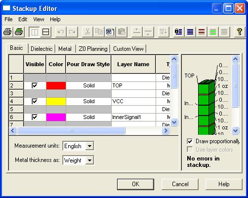
5 Setup/planning Board Stackup Design Signal Integrity Impedance Highest impedance will drive layer thicknesses Need reference planes for uniform impedance Loss Drives trace widths > layer thicknesses Crosstalk Drives spacing requirements and routing density Power Integrity Need enough thick planes to minimize DC drop Need closely-spaced plane pairs for AC needs Need stitching vias to relieve current choke points EMI/EMC Need solid reference planes throughout stackup capacitor

6 Design Considerations Layout/Route Avoid crossing splits in reference planes (discontinuities) Minimize Inter Symbol Interference (ISI) using matched Impedances Minimize Crosstalk by isolating sensitive bits (ie. Strobes) Match traces within byte lanes (DQ, DM, DQS) to minimize skews Power Supplies Use precision resistors for V REF Short/Wide traces to minimize L and loss 15~25mil clearance from V REF to adjacent traces to minimize coupling Decouple high frequency Power Supply noise w/caps Signaling DQ Driver Impedance Matching with proper drive strengths ODT is a must for better Signal Integrity (if not used then use T-branches or dumping resistor to minimize reflections Choose termination carefully to balance power consumption, signal swing, and reflection Use 2T timing for Address/Command


7 Signal Integrity Analysis Signal Integrity Crosstalk EMC Eye Diagrams Sweep Parameters Impedance/Stackup Planning Multi-Board

8 DDRx Fly-By Topology Write Leveling Controller Delays DQ signals internally DQ & DQS signals are sent Level with the Addr/CLK
9 Overview DDR3 vs. DDR4 VDD/VDDQ/VPP DDR3 DDR4 Comments 1.5/1.5/NA (1.35/1.35/NA) 1.2/1.2/2.5 Up to 20% power saving Clock Frequencies MHz MHz+ Higher BW CAS Latency 5~14 9~24 Vref VDDQ/2 (Ext) Internal DQ Validation Setup/Hold Data Eye Borrowed from SERDES Data Termination VDDQ/2 (VTT) VDDQ Asymmetric Term. Add/Cmd/Termination VDDQ/2 (VTT) VDDQ/2 I/O Standard SSTL15 POD12 Power savings on 1 bits On Chip Error Detection No Parity (Cmd/Add) CRC (DQ) Server Class Bank Grouping No 4 Ping-Pong for efficient use
10 Overview LPDDR3 vs LPDDR4 LPDDR3 LPDDR4 Comments CLK MHz MHz 2x speed (possibly more) Bandwidth 12.8GB/s (2ch) 25.6GB/s (2ch) Higher BW VDD2/VDDQ/VDD1 1.2/1.2/ /1.1/1.8 Power reduced 10% I/O Interface HSUL LVSTL 40% I/O Power reduction DQ ODT Vtt Term VSSQ Term vs. POD CA ODT No term VSS Term (optional) Vref External Internal DDR4 to use Pseudo Open Drain (POD) Address, Command, Control continue to be SSTL LPDDR4 to use Low Voltage Swing Terminated Logic (LVSTL) Both Data and Address

11 Overview Speed related Eye challenges Semicon West: High Performance & Low Power Memory Trends SK Hynix
12 New Drive Standards Difference DDR4 DDR
13 New Drive Standards Why? Current still flows when driving low I DDR4 I DDR
14 New Drive Standards Why? No current draw when driving a high No Current DDR4 I DDR
15 Power Savings with DBI Ensure more 1 s than 0 s with POD If more than 4 bits in a byte are 0, toggle bits DBI (Data Bit Inversion) shared with DM => only one feature enabled DBI pin is I/O (affects both reads and writes)

16 PreLayout SI Simulation

 Diff pair rules 2014 17")
17 DDRx Routing Guidelines Constraint-driven routing Designer knows where the traces should be routed Precise location of traces & vias Control style of routing incl serpentines Things to observe while routing DDRx Width & clearance rules Placement intentions Netline organization Layer restrictions Pad/via entry rules (angle, size) Diff pair rules
 2014")
18 Using Sketch routing with DDR3 (video)

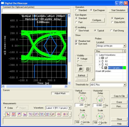
19 Simple Comparison Controller -> 50 Ohm T-Line -> DRAM Vary DRAM s ODT to see center level of eye 2400Mbps Data rate

20 DDR3 sweeping Rx ODT No change in Center of Eye with ODT

21 DDR4 Eye shifting Eye center shifts with ODT change

22 LPDDR4 Eye shifting Eye center shifts with ODT change

23 Xilinx VCU108 UltraScale Dev Board


24 Altera Aria10GX FPGA Dev Board DDR4 Module
 from PWR to ICs (Active Devices) Including PCBs and packages Planes, routed traces, and decoupling capacitors Deliver adequate power from DC->HF Minimize EMI issues")
25 What is Power Integrity? What is a Power Distribution Network (PDN)? The path (or interconnects) from PWR to ICs (Active Devices) Including PCBs and packages Planes, routed traces, and decoupling capacitors Deliver adequate power from DC->HF Minimize EMI issues Provide low-noise reference path for signaling Bypass capacitor Active device Power planes PCB VRM Test point 2 Test point
26 Plane Design & the PDN Meeting Power Integrity requirements Design PDN (path from power supply to ICs) of low impedance As if an ideal voltage source were directly connected to ICs Use impedance to represent and measure PDN quality Power Delivery Path Die Chip to Package Bumps Package Package to Board Bump and/or Connectors PCB PCB Routing


27 Power Integrity Analysis DC Drop Analysis Excessive Voltage Drop & High Current Densities Batch Analysis of Supply Nets AC Power Plane Analysis Capacitor Selection/Mounting Power Supply Impedance Plane Noise Analysis Voltage Ripples
 Reduce Product Costs Minimizing capacitor BOM (more Caps is worse) Reducing PCB size and")

28 Power Integrity Optimization (Why?) Reduce Product Costs Minimizing capacitor BOM (more Caps is worse) Reducing PCB size and layer count Eliminating design iterations Up-front PDN planning & Improve time-to-results Improve Product Reliability Identifying excessive voltage drop and high current densities at DC Providing stable AC power through capacitor decoupling


29 DC Drop and Thermal Analysis Identify Failures Easily Voltage drop magnitude is easily measured Excessive current density is identified clearly Determine if current density is causing thermal failure Create an Optimized Solution How much copper is needed? Optimize component placement? Are additional stitching vias required?

30 Power Integrity/Thermal Integrity Effects Analyze Joule Heating effects in traces Identify/localize sensitive area on board Minimize field failures and increase product reliability
31 Power Integrity Effects

32 Power Integrity Effects from DDR3 switching Signal held high PDN From DDR3 Board Remaining signals 2400MT/s DQS 1.2GHz

33 Power Integrity Effects from DDR3 switching 150mV noise from switching of other bits in lane


34 Integrated Design Flow Tight validation for Pre/Post Layout Minimize errors, increase accuracy Reduce risk and field failures Lower cost and reduce time-to-market SI/PI/Thermal Simulation Pre/Post Architectural/Technology Investigation Performance/Feasibility Analysis Noise/Crosstalk/Termination/EMI Constraints Constraints Stackup/Placements Length/Impedance/via Board Schematic Library/Symbols Design Variants Layout/Route Design Constraints
35 Contact Info EDA Direct Inc. (408) (888) 669-9EDA To enroll for our upcoming seminars, workshops, training classes, and view demo videos of our products visit
Designing High-Speed Memory Subsystem DDR. using. Cuong Nguyen. Field Application Engineer
 Designing High-Speed Memory Subsystem using DDR Cuong Nguyen Field Application Engineer cuong@edadirect.com www.edadirect.com 2014 1 Your Design for Excellence Partner Since 1997 EDA Direct has helped
Electrical optimization and simulation of your PCB design
 Electrical optimization and simulation of your PCB design Steve Gascoigne Senior Consultant at Mentor Graphics Zagreb, 10. lipnja 2015. Copyright CADCAM Group 2015 The Challenge of Validating a Design..
DDR4 Design And Verification In Hyperlynx LINESIM/Boardsim
 DDR4 Design And Verification In Hyperlynx LINESIM/Boardsim Rod Strange Business Development Manager Teraspeed Consulting A Division of Samtec April 2016 Outline Objective/Goal DDR4 vs. DDR3 from the SI/PI
Modern Memory Interfaces (DDR3) Design with ANSYS Virtual Prototype approach
 Design with ANSYS Virtual Prototype approach") Modern Memory Interfaces (DDR3) Design with ANSYS Virtual Prototype approach 1 ANSYS, Inc. Proprietary 2012 ANSYS, Inc. November 14, 2012 1-1 Agenda DDR Design Challenges How does simulation solve these
Modern Memory Interfaces (DDR3) Design with ANSYS Virtual Prototype approach 1 ANSYS, Inc. Proprietary 2012 ANSYS, Inc. November 14, 2012 1-1 Agenda DDR Design Challenges How does simulation solve these
LPDDR4: Evolution for new Mobile World
 LPDDR4: Evolution for new Mobile World 2013.08.06 JungYong(JY) Choi Senior Manager Samsung Semiconductor Inc. 1 / 22 Legal Disclaimer This presentation is intended to provide information concerning memory
Board Design Guidelines for PCI Express Architecture
 Board Design Guidelines for PCI Express Architecture Cliff Lee Staff Engineer Intel Corporation Member, PCI Express Electrical and Card WGs The facts, techniques and applications presented by the following
Technical Note LPSDRAM Unterminated Point-to-Point System Design: Layout and Routing Tips
 Introduction Technical Note LPSDRAM Unterminated Point-to-Point System Design: Layout and Routing Tips Introduction Background Low-power (LP) SDRAM, including both low-power double data rate (LPDDR) and
Symbol Parameter Min Typ Max VDD_CORE Core power 0.9V 1.0V 1. 1V. VDD33 JTAG/FLASH power 2.97V 3.3V 3.63V
 1 Introduction The user guide provides guidelines on how to help you successfully design the CME-M7 board which includes the power supply, configuration, clock, DDR2 or DDR3, high speed USB, LVDS and ADC
Optimization of Modern Memory
 System Design, Verificationand and Optimization of Modern Memory Interfaces (DDR3) Santa Clara, Aug 23 rd 2011 Robert Myoung Sr. Application Engineer 1 Agenda Introduction ECAD Geometry Translation SI/PI
QDR II SRAM Board Design Guidelines
 8 emi_dg_007 Subscribe The following topics provide guidelines for you to improve your system's signal integrity and layout guidelines to help successfully implement a QDR II or QDR II+ SRAM interface
Hardware Design Guidelines for Freescale s High-Performance Digital Signal Processors
 June 2010 Hardware Design Guidelines for Freescale s High-Performance Digital Signal Processors Colin McEwan Systems and Applications Engineer Agenda Introduction and Review Agenda The Freescale AMC ECO-System
High-Speed Layout Guidelines for Reducing EMI for LVDS SerDes Designs. I.K. Anyiam
 High-Speed Layout Guidelines for Reducing EMI for LVDS SerDes Designs I.K. Anyiam 1 Introduction LVDS SerDes helps to reduce radiated emissions, but does not completely eliminate them EMI prevention must
What s New in HyperLynx 8.0
 What s New in HyperLynx 8.0 Copyright Mentor Graphics Corporation 2009 All Rights Reserved. Mentor Graphics, Board Station XE Flow, ViewDraw, Falcon Framework, IdeaStation, ICX and Tau are registered trademarks
Signal Integrity Comparisons Between Stratix II and Virtex-4 FPGAs
 White Paper Introduction Signal Integrity Comparisons Between Stratix II and Virtex-4 FPGAs Signal integrity has become a critical issue in the design of high-speed systems. Poor signal integrity can mean
DDR System Simulation: What Issue to Simulate
 DDR System Simulation: What Issue to Simulate Asian IBIS Summit Tokyo, Japan November 17, 2017 Shinichi Maeda 1 JEDEC DDR Specifications DDR DDR2 DDR3 DDR3L DDR3U DDR4 Vdd 2.5 1.8 1.5 1.35 1.25 1.2(IO)
Technical Note DDR2 (Point-to-Point) Package Sizes and Layout Basics
 Package Sizes and Layout Basics") Introduction Technical Note DDR2 (Point-to-Point) Package Sizes and Layout Basics Introduction Point-to-point designers face many challenges when laying out a new printed circuit board (PCB). The designer
Introduction Technical Note DDR2 (Point-to-Point) Package Sizes and Layout Basics Introduction Point-to-point designers face many challenges when laying out a new printed circuit board (PCB). The designer
Allegro Sigrity SI Streamlining the creation of high-speed interconnect on digital PCBs and IC packages
 Streamlining the creation of high-speed interconnect on digital PCBs and IC packages The Cadence Allegro Sigrity signal integrity (SI) integrated high-speed design and analysis environment streamlines
PC2-5300/PC DDR2 SDRAM Unbuffered DIMM Design Specification Revision 3.1 October 2008
 Page 4.20.13-1 4.20.13-240-Pin PC2-5300/PC2-6400 DDR2 SDRAM Unbuffered DIMM Design Specification PC2-5300/PC2-6400 DDR2 SDRAM Unbuffered DIMM Design Specification Revision 3.1 October 2008 JEDED Standard
DDR4: Designing for Power and Performance
 DDR4: Designing for Power and Performance Agenda Comparison between DDR3 and DDR4 Designing for power DDR4 power savings Designing for performance Creating a data valid window Good layout practices for
Interfacing the RC32438 with DDR SDRAM Memory
 Interfacing the RC32438 with DDR SDRAM Memory Application Note AN-371 Revision History By Kasi Chopperla and Harold Gomard July 3, 2003: Initial publication. October 23, 2003: Added DDR Loading section.
Implementing LVDS in Cyclone Devices
 Implementing LVDS in Cyclone Devices March 2003, ver. 1.1 Application Note 254 Introduction Preliminary Information From high-speed backplane applications to high-end switch boxes, LVDS is the technology
Best practices for EMI filtering and IC bypass/decoupling applications
 X2Y Component Connection and PCB Layout Guidelines Best practices for EMI filtering and IC bypass/decoupling applications X2Y Attenuators, LLC 1 Common X2Y Circuit Uses EMI FILTERING Conducted and Radiated
High-speed, high-bandwidth DRAM memory bus with Crosstalk Transfer Logic (XTL) interface. Outline
 interface. Outline") High-speed, high-bandwidth DRAM memory bus with Crosstalk Transfer Logic (XTL) interface Hideki Osaka Hitachi Ltd., Kanagawa, Japan oosaka@sdl.hitachi.co.jp Toyohiko Komatsu Hitachi Ltd., Kanagawa, Japan
High-speed, high-bandwidth DRAM memory bus with Crosstalk Transfer Logic (XTL) interface Hideki Osaka Hitachi Ltd., Kanagawa, Japan oosaka@sdl.hitachi.co.jp Toyohiko Komatsu Hitachi Ltd., Kanagawa, Japan
MAX 10 FPGA Signal Integrity Design Guidelines
 2014.12.15 M10-SIDG Subscribe Today s complex FPGA system design is incomplete without addressing the integrity of signals coming in to and out of the FPGA. Simultaneous switching noise (SSN) often leads
Technical Note. ONFI 4.0 Design Guide. Introduction. TN-29-83: ONFI 4.0 Design Guide. Introduction
 Introduction Technical Note ONFI 4.0 Design Guide Introduction The ONFI 4.0 specification enables high data rates of 667 MT/s and 800 MT/s. These high data rates, along with lower input/output capacitance,
REV CHANGE DESCRIPTION NAME DATE. A Release
 REV CHANGE DESCRIPTION NAME DATE A Release 7-25-12 Any assistance, services, comments, information, or suggestions provided by SMSC (including without limitation any comments to the effect that the Company
An Innovative Simulation Workflow for Debugging High-Speed Digital Designs using Jitter Separation
 An Innovative Simulation Workflow for Debugging High-Speed Digital Designs using Jitter Separation C. Chastang, A. Amédéo V. Poisson, P. Grison, F. Demuynck C. Gautier, F. Costa Thales Communications &
Five Emerging DRAM Interfaces You Should Know for Your Next Design
 Five Emerging DRAM Interfaces You Should Know for Your Next Design By Gopal Raghavan, Cadence Design Systems Producing DRAM chips in commodity volumes and prices to meet the demands of the mobile market
Breakthrough Insight into DDR4/LPDDR4 Memory Greater Than 2400 Mb/s
 Breakthrough Insight into DDR4/LPDDR4 Memory Greater Than 2400 Mb/s January 2015 Jennie Grosslight Product Manager Agenda Overview Benefits and challenges for DDR4 and LPDDR4 >2400Mb/s Breakthrough Insight
Implementing Bus LVDS Interface in Cyclone III, Stratix III, and Stratix IV Devices
 Implementing Bus LVDS Interface in Cyclone III, Stratix III, and Stratix IV Devices November 2008, ver. 1.1 Introduction LVDS is becoming the most popular differential I/O standard for high-speed transmission
IDT PEB383 QFP Board Design Guidelines
 IDT PEB383 QFP Board Design Guidelines February 2010 6024 Silver Creek Valley Road, San Jose, California 95138 Telephone: (800) 345-7015 (408) 284-8200 FAX: (408) 284-2775 Printed in U.S.A. 2009 GENERAL
LE4ASS21PEH 16GB Unbuffered 2048Mx64 DDR4 SO-DIMM 1.2V Up to PC CL
 LE4ASS21PEH 16GB Unbuffered 2048Mx64 DDR4 SO-DIMM 1.2V Up to PC4-2133 CL 15-15-15 General Description This Legacy device is a JEDEC standard unbuffered SO-DIMM module, based on CMOS DDR4 SDRAM technology,
HyperLynx DDRx Interface Analysis. Student Workbook
 HyperLynx DDRx Interface Analysis Student Workbook 2017 Mentor Graphics Corporation All rights reserved. This document contains information that is trade secret and proprietary to Mentor Graphics Corporation
IP1001 LF DESIGN & LAYOUT GUIDELINES
 Index 1 Purpose...2 2 Magnetic trace routing...2 3 Power Supply Plane & GND Plane...3 4 PHY interface...3 5 Trace routing & Placement...3 6 ESD protection...3 7 EMI Supression...3 1/7 April 17 2008. Ver:1.5
High Performance DDR4 interfaces with FPGA Flexibility. Adrian Cosoroaba and Terry Magee Xilinx, Inc.
 High Performance DDR4 interfaces with FPGA Flexibility Adrian Cosoroaba and Terry Magee Xilinx, Inc AGENDA System Requirements for FPGA based systems Higher Bandwidth, Increased Flexibility, Lower Power
Graser User Conference Only
 High-Speed Interface Driven PCB Design (Net Group, Aixx, Floorplanning etc) Mika Ho / Graser 31/Oct/2014 Topic Chapter One An Interface Example DDRx An Example: Timing Relationship for DDR3 Case Description
8. Selectable I/O Standards in Arria GX Devices
 8. Selectable I/O Standards in Arria GX Devices AGX52008-1.2 Introduction This chapter provides guidelines for using industry I/O standards in Arria GX devices, including: I/O features I/O standards External
2-Channel 2-Layer Inner-Stack Memory-module Design for LPDDR2/3 DRAM
 SPI2012 2-Channel 2-Layer Inner-Stack Memory-module Design for LPDDR2/3 DRAM May 14, 2012 Jongjoo Lee jjdragon@ieee.org Joon Ki Paek and Joonhee Lee Solution Development Team Memory Division Samsung Electronics
PC2700 Unbuffered DDR MicroDIMM Reference Design Specification Revision 0.11 March 25, 2001 JC42.5 Item # BOARD OF DIRECTORS BALLOT
 PC2700 Unbuffered MicroDIMM Reference Design Specification Revision 0.11 March 25, 2001 JC42.5 Item #1194.01 BOARD OF DIRECTORS BALLOT Unbuffered MicroDIMM Contents 1. Product Description... 3 Product
Organization Row Address Column Address Bank Address Auto Precharge 128Mx8 (1GB) based module A0-A13 A0-A9 BA0-BA2 A10
 based module A0-A13 A0-A9 BA0-BA2 A10") GENERAL DESCRIPTION The Gigaram is ECC Registered Dual-Die DIMM with 1.25inch (30.00mm) height based on DDR2 technology. DIMMs are available as ECC modules in 256Mx72 (2GByte) organization and density,
GENERAL DESCRIPTION The Gigaram is ECC Registered Dual-Die DIMM with 1.25inch (30.00mm) height based on DDR2 technology. DIMMs are available as ECC modules in 256Mx72 (2GByte) organization and density,
CrossLink Hardware Checklist Technical Note
 FPGA-TN-02013 Version 1.1 August 2017 Contents Acronyms in This Document... 3 Introduction... 4 Power Supplies... 5 CrossLink MIPI D-PHY and PLL Power Supplies... 5 Power Estimation... 6 Configuration
ASIX USB-to-LAN Applications Layout Guide
 ASIX USB-to-LAN Applications Revision 1.0 Dec. 11th, 2007 1 Revision Date Description 1.0 2007/12/11 New release. ASIX USB-to-LAN Applications Revision History 2 Content 1. Introduction...4 2. 4-Layer
1. Introduction Reference Schematics Pin Control and Configuration Guideline (Pin Control Mode for ZB48 package)...
...") Design Guide for DisplayPort Source Application PIEQXDP0 Table of Contents. Introduction... 2 2. Reference Schematics.... Pin Control and Configuration Guideline (Pin Control Mode for ZB8 package)....
Design Guide for DisplayPort Source Application PIEQXDP0 Table of Contents. Introduction... 2 2. Reference Schematics.... Pin Control and Configuration Guideline (Pin Control Mode for ZB8 package)....
89HPES24T3G2 Hardware Design Guide
 89H Hardware Design Guide Notes Introduction This document provides system design guidelines for IDT 89H PCI Express (PCIe ) 2. base specification compliant switch device. The letters "G2" within the device
TITLE. on SSD Boards. Image. Topic: Topic: Seong-Jin Mun, (Samsung Electronics Inc.)
") TITLE Topic: Far-Field o Nam elementum EMI commodo Analysis mattis. Pellentesque Methodology and Verification on SSD Boards Topic: o malesuada blandit euismod. Seong-Jin Mun, (Samsung Electronics Inc.)
TITLE Topic: Far-Field o Nam elementum EMI commodo Analysis mattis. Pellentesque Methodology and Verification on SSD Boards Topic: o malesuada blandit euismod. Seong-Jin Mun, (Samsung Electronics Inc.)
Interfacing FPGAs with High Speed Memory Devices
 Interfacing FPGAs with High Speed Memory Devices 2002 Agenda Memory Requirements Memory System Bandwidth Do I Need External Memory? Altera External Memory Interface Support Memory Interface Challenges
IMME256M64D2DUD8AG (Die Revision E) 2GByte (256M x 64 Bit)
 2GByte (256M x 64 Bit)") Product Specification Rev. 1.0 2015 IMME256M64D2DUD8AG (Die Revision E) 2GByte (256M x 64 Bit) 2GB DDR2 Unbuffered DIMM By ECC DRAM RoHS Compliant Product Product Specification 1.0 1 IMME256M64D2DUD8AG
Product Specification Rev. 1.0 2015 IMME256M64D2DUD8AG (Die Revision E) 2GByte (256M x 64 Bit) 2GB DDR2 Unbuffered DIMM By ECC DRAM RoHS Compliant Product Product Specification 1.0 1 IMME256M64D2DUD8AG
Optical SerDes Test Interface for High-Speed and Parallel Testing
 June 7-10, 2009 San Diego, CA SerDes Test Interface for High-Speed and Parallel Testing Sanghoon Lee, Ph. D Sejang Oh, Kyeongseon Shin, Wuisoo Lee Memory Division, SAMSUNG ELECTRONICS Why Interface? High
90000 DSO/DSA Series Oscilloscopes
 DDR4 Keysight Compliance Infiniium Test Bench 90000 DSO/DSA Series Oscilloscopes ADS DDR4 DesignGuide and Compliance Test Bench 1 Contents Installing the DDR4 Compliance Test Bench... 2 Prerequisites...
IMME256M64D2SOD8AG (Die Revision E) 2GByte (256M x 64 Bit)
 2GByte (256M x 64 Bit)") Product Specification Rev. 1.0 2015 IMME256M64D2SOD8AG (Die Revision E) 2GByte (256M x 64 Bit) 2GB DDR2 Unbuffered SO-DIMM By ECC DRAM RoHS Compliant Product Product Specification 1.0 1 IMME256M64D2SOD8AG
Product Specification Rev. 1.0 2015 IMME256M64D2SOD8AG (Die Revision E) 2GByte (256M x 64 Bit) 2GB DDR2 Unbuffered SO-DIMM By ECC DRAM RoHS Compliant Product Product Specification 1.0 1 IMME256M64D2SOD8AG
4. Selectable I/O Standards in Stratix II and Stratix II GX Devices
 4. Selectable I/O Standards in Stratix II and Stratix II GX Devices SII52004-4.6 Introduction This chapter provides guidelines for using industry I/O standards in Stratix II and Stratix II GX devices,
Tsi381 Board Design Guidelines
 Tsi381 Board Design Guidelines September 2009 6024 Silver Creek Valley Road, San Jose, California 95138 Telephone: (800) 345-7015 (408) 284-8200 FAX: (408) 284-2775 Printed in U.S.A. 2009, Inc. GENERAL
Tsi384 Board Design Guidelines
 Tsi384 Board Design Guidelines September 2009 6024 Silver Creek Valley Road, San Jose, California 95138 Telephone: (800) 345-7015 (408) 284-8200 FAX: (408) 284-2775 Printed in U.S.A. 2009, Inc. GENERAL
ADQVD1B16. DDR2-800+(CL4) 240-Pin EPP U-DIMM 2GB (256M x 64-bits)
 240-Pin EPP U-DIMM 2GB (256M x 64-bits)") General Description ADQVD1B16 DDR2-800+(CL4) 240-Pin EPP U-DIMM 2GB (256M x 64-bits) The ADATA s ADQVD1B16 is a 256Mx64 bits 2GB(2048MB) DDR2-800(CL4) SDRAM EPP memory module, The SPD is programmed to
General Description ADQVD1B16 DDR2-800+(CL4) 240-Pin EPP U-DIMM 2GB (256M x 64-bits) The ADATA s ADQVD1B16 is a 256Mx64 bits 2GB(2048MB) DDR2-800(CL4) SDRAM EPP memory module, The SPD is programmed to
Session 4a. Burn-in & Test Socket Workshop Burn-in Board Design
 Session 4a Burn-in & Test Socket Workshop 2000 Burn-in Board Design BURN-IN & TEST SOCKET WORKSHOP COPYRIGHT NOTICE The papers in this publication comprise the proceedings of the 2000 BiTS Workshop. They
2. Recommended Design Flow
 2. Recommended Design Flow This chapter describes the Altera-recommended design low or successully implementing external memory interaces in Altera devices. Altera recommends that you create an example
EXAMINING THE IMPACT OF SPLIT PLANES ON SIGNAL AND POWER INTEGRITY
 EXAMINING THE IMPACT OF SPLIT PLANES ON SIGNAL AND POWER INTEGRITY Jason R. Miller, Gustavo J. Blando, Roger Dame, K. Barry A. Williams and Istvan Novak Sun Microsystems, Burlington, MA 1 AGENDA Introduction
This application note is written for a reader that is familiar with Ethernet hardware design.
 AN 14.8 LAN8700/LAN8700I and LAN8187/LAN8187I Ethernet PHY Layout Guidelines 1 Introduction 1.1 Audience 1.2 Overview The LAN8700/LAN8700I and LAN8187/LAN8187I are highly-integrated devices designed for
Memory Module Specifications KVR667D2Q8F5K2/8G. 8GB (4GB 512M x 72-Bit x 2 pcs.) PC CL5 ECC 240-Pin FBDIMM Kit DESCRIPTION SPECIFICATIONS
 PC CL5 ECC 240-Pin FBDIMM Kit DESCRIPTION SPECIFICATIONS") Memory Module Specifications KVR667DQ8F5K/8G 8GB (4GB 5M x 7-Bit x pcs.) PC-5300 CL5 ECC 40- FBDIMM Kit DESCRIPTION s KVR667DQ8F5K/8G is a kit of two 4GB (5M x 7-bit) PC-5300 CL5 SDRAM (Synchronous DRAM)
Memory Module Specifications KVR667DQ8F5K/8G 8GB (4GB 5M x 7-Bit x pcs.) PC-5300 CL5 ECC 40- FBDIMM Kit DESCRIPTION s KVR667DQ8F5K/8G is a kit of two 4GB (5M x 7-bit) PC-5300 CL5 SDRAM (Synchronous DRAM)
Application Note. PCIE-RA Series Final Inch Designs in PCI Express Applications Generation GT/s
 PCIE-RA Series Final Inch Designs in PCI Express Applications Generation 3-8.0 GT/s Copyrights and Trademarks Copyright 2012, Inc. COPYRIGHTS, TRADEMARKS, and PATENTS Final Inch is a trademark of, Inc.
Apache s Power Noise Simulation Technologies
 Enabling Power Efficient i Designs Apache s Power Noise Simulation Technologies 1 Aveek Sarkar VP of Support Apache Design Inc, A wholly owned subsidiary of ANSYS Trends in Today s Electronic Designs Low-power
Multi-Drop LVDS with Virtex-E FPGAs
 Multi-Drop LVDS with Virtex-E FPGAs XAPP231 (Version 1.0) September 23, 1999 Application Note: Jon Brunetti & Brian Von Herzen Summary Introduction Multi-Drop LVDS Circuits This application note describes
RML1531MH48D8F-667A. Ver1.0/Oct,05 1/8
 DESCRIPTION The Ramaxel RML1531MH48D8F memory module family are low profile Unbuffered DIMM modules with 30.48mm height based DDR2 technology. DIMMs are available as ECC (x72) modules. The module family
2GB DDR3 SDRAM 72bit SO-DIMM
 2GB 72bit SO-DIMM Speed Max CAS Component Number of Part Number Bandwidth Density Organization Grade Frequency Latency Composition Rank 78.A2GCF.AF10C 10.6GB/sec 1333Mbps 666MHz CL9 2GB 256Mx72 256Mx8
Application Note. PCIE-EM Series Final Inch Designs in PCI Express Applications Generation GT/s
 PCIE-EM Series Final Inch Designs in PCI Express Applications Generation 3-8.0 GT/s Copyrights and Trademarks Copyright 2015, Inc. COPYRIGHTS, TRADEMARKS, and PATENTS Final Inch is a trademark of, Inc.
Interfacing RLDRAM II with Stratix II, Stratix,& Stratix GX Devices
 Interfacing RLDRAM II with Stratix II, Stratix,& Stratix GX Devices November 2005, ver. 3.1 Application Note 325 Introduction Reduced latency DRAM II (RLDRAM II) is a DRAM-based point-to-point memory device
PI2EQX6874ZFE 4-lane SAS/SATA ReDriver Application Information
 Contents General Introduction How to use pin strap and I2C control External Components Requirement Layout Design Guide Power Supply Bypassing Power Supply Sequencing Equalization Setting Output Swing Setting
DDR2 SDRAM UDIMM MT8HTF12864AZ 1GB
 Features DDR2 SDRAM UDIMM MT8HTF12864AZ 1GB For component data sheets, refer to Micron's Web site: www.micron.com Figure 1: 240-Pin UDIMM (MO-237 R/C D) Features 240-pin, unbuffered dual in-line memory
REV CHANGE DESCRIPTION NAME DATE. A Release
 REV CHANGE DESCRIPTION NAME DATE A Release 1-20-17 Any assistance, services, comments, information, or suggestions provided by Microchip (including without limitation any comments to the effect that the
Optimum Placement of Decoupling Capacitors on Packages and Printed Circuit Boards Under the Guidance of Electromagnetic Field Simulation
 Optimum Placement of Decoupling Capacitors on Packages and Printed Circuit Boards Under the Guidance of Electromagnetic Field Simulation Yuzhe Chen, Zhaoqing Chen and Jiayuan Fang Department of Electrical
KVR667D2D8F5/1G 1GB 128M x 72-Bit PC CL5 ECC 240-Pin FBDIMM
 Memory Module Specifications KVR667D2D8F5/1G 1GB 128M x 72-Bit PC2-5300 CL5 ECC 240- FBDIMM Description: This document describes ValueRAM's 1GB (128M x 72-bit) PC2-5300 CL5 (Synchronous DRAM) "fully buffered"
SDRAM DDR3 256MX8 ½ Density Device Technical Note
 SDRAM DDR3 256MX8 ½ Density Device Technical Note Introduction This technical note provides an overview of how the SGG128M8V79DG8GQF-15E DDR3 SDRAM device is configured and tested as a 1Gb device. This
Designing and Verifying Future High Speed Busses
 Designing and Verifying Future High Speed Busses Perry Keller Agilent Technologies Gregg Buzard December 12, 2000 Agenda Bus Technology Trends and Challenges Making the transition: Design and Test of DDR
TABLE OF CONTENTS 1.0 PURPOSE INTRODUCTION ESD CHECKS THROUGHOUT IC DESIGN FLOW... 2
 TABLE OF CONTENTS 1.0 PURPOSE... 1 2.0 INTRODUCTION... 1 3.0 ESD CHECKS THROUGHOUT IC DESIGN FLOW... 2 3.1 PRODUCT DEFINITION PHASE... 3 3.2 CHIP ARCHITECTURE PHASE... 4 3.3 MODULE AND FULL IC DESIGN PHASE...
AN INTRODUCTION TO HYPERLYNX SI/PI TECHNOLOGY
 AN INTRODUCTION TO HYPERLYNX SI/PI TECHNOLOGY BY STEVE KAUFER, MENTOR H I G H S P E E D D E S I G N W H I T E P A P E R OVERVIEW Digital designers are now required to make the leap from time domain to
MDI for 4x25G Copper and Fiber Optic IO. Quadra (CFP4 proposal) Connector System
 Connector System") MDI for 4x25G Copper and Fiber Optic IO Quadra (CFP4 proposal) Connector System Nov 7, 2011 Nathan Tracy, TE Connectivity Tom Palkert, Molex 4x25Gb/s MDI Potential Requirements Critical Needs: Excellent
MDI for 4x25G Copper and Fiber Optic IO Quadra (CFP4 proposal) Connector System Nov 7, 2011 Nathan Tracy, TE Connectivity Tom Palkert, Molex 4x25Gb/s MDI Potential Requirements Critical Needs: Excellent
Fairchild Semiconductor Application Note December 2000 Revised June What is LVDS? FIGURE 2. Driver/Receiver Schematic
 LVDS Fundamentals Introduction With the recent developments in the communications market, the demand for throughput is becoming increasingly more crucial. Although older differential technologies provide
2. Control Pin Functions and Applications
 IMARY CONTROL ( PIN) Module Enable / Disable. The module can be disabled by pulling the below 2.3 V with respect to the Input. This should be done with an open-collector transistor, relay, or optocoupler.
REV CHANGE DESCRIPTION NAME DATE. A Release B Increased +1.2V Capacitor Value & VDD12A Cap Requirement
 REV CHANGE DESCRIPTION NAME DATE A Release 8-1-16 B Increased +1.2V Capacitor Value & VDD12A Cap Requirement 1-16-17 Any assistance, services, comments, information, or suggestions provided by Microchip
SEAM-RA/SEAF-RA Series Final Inch Designs in PCI Express Applications Generation GT/s
 SEAM-RA/SEAF-RA Series Final Inch Designs in PCI Express Applications Generation 3-8.0 GT/s Copyrights and Trademarks Copyright 2011 Samtec, Inc. Developed in conjunction with Teraspeed Consulting Group
AN_8430_002 April 2011
 A Maxim Integrated Products Brand 78Q8430 10/100 Ethernet MAC and PHY APPLICATION NOTE AN_8430_002 April 2011 Introduction 78Q8430 Layout Guidelines The TSC 78Q8430 is a single chip 10Base-T/100Base-TX
PI2EQX6804-ANJE Four-lane SAS/SATA ReDriver Application Information May 13, 2011
 Contents General Introduction How to use pin strap and I2C control External Components Requirement Layout Design Guide Power Supply Bypassing Power Supply Sequencing Equalization Setting Output Swing Setting
SC64G1A08. DDR3-1600F(CL7) 240-Pin XMP(ver 2.0) U-DIMM 1GB (128M x 64-bits)
 240-Pin XMP(ver 2.0) U-DIMM 1GB (128M x 64-bits)") SC64G1A08 DDR3-1600F(CL7) 240-Pin XMP(ver 2.0) U-DIMM 1GB (128M x 64-bits) General Description The ADATA s SC64G1A08 is a 128Mx64 bits 1GB(1024MB) DDR3-1600(CL7) SDRAM XMP (ver 2.0) memory module, The
SC64G1A08 DDR3-1600F(CL7) 240-Pin XMP(ver 2.0) U-DIMM 1GB (128M x 64-bits) General Description The ADATA s SC64G1A08 is a 128Mx64 bits 1GB(1024MB) DDR3-1600(CL7) SDRAM XMP (ver 2.0) memory module, The
PC2-6400/PC2-5300/PC2-4200/PC Registered DIMM Design Specification Revision 3.40 August 2006
 JEDEC Standard No. 21C Page 4.20.10-1 4.20.10-240-Pin PC-6400/PC2-5300/PC2-4200/PC2-3200 DDR2 SDRAM ed DIMM Design Specification PC2-6400/PC2-5300/PC2-4200/PC2-3200 ed DIMM Design Specification Revision
Implementing Multi-Gigabit Serial Links in a System of PCBs
 Implementing Multi-Gigabit Serial Links in a System of PCBs Donald Telian April 2002 rev. 1.2 About the Author Donald Telian Technologist, Cadence Design Systems Donald has been involved in high-speed
PI6C GND REF_IN+ V TH V REF-AC REF_IN- Q0+ Q0- Q1+ Q1- VDD. 6 GHz / 12 Gbps Clock / Data Fanout Buffer with Internal Termination.
 Features ÎÎInput Clock Frequency up to 6 GHz Typical ÎÎMaximum Input Data Rate up to 12 Gbps Typical ÎÎ2 pairs of differential CML outputs ÎÎLow additive jitter, < 0.05ps (max) ÎÎInput accepts: CML, LVDS,
DM9051NP Layout Guide
 NP Version: 1.1 Technical Reference Manual Davicom Semiconductor, Inc Version: NP-LG-V11 1 1. Placement, Signal and Trace Routing Place the 10/100M magnetic as close as possible to the (no more than 20mm)
Integrating ADS into a High Speed Package Design Process
 Integrating ADS into a High Speed Package Design Process Page 1 Group/Presentation Title Agilent Restricted Month ##, 200X Agenda High Speed SERDES Package Design Requirements Performance Factor and Design
Cadence Power Integrity Solutions For PCBs and IC Packages. May 2013
 Cadence Power Integrity Solutions For PCBs and IC Packages May 2013 Simultaneous Switching Noise (SSN) A Power Integrity Issue Design with decaps intentionally removed to demonstrate how poor PI performance
100GbE Architecture - Getting There... Joel Goergen Chief Scientist
 100GbE Architecture - Getting There... Joel Goergen Chief Scientist April 26, 2005 100GbE Architecture - Getting There Joel Goergen Force10 Networks joel@force10networks.com Subject : 100GbE Architecture
External Memory Interfaces Intel Arria 10 FPGA IP User Guide
 External Memory Interfaces Intel Arria 10 FPGA IP User Guide Updated for Intel Quartus Prime Design Suite: 18.0 Subscribe Send Feedback Latest document on the web: PDF HTML Contents Contents 1. External
W5100 Layout Guide version 1.0
 version 1.0 2009 WIZnet Co., Inc. All Rights Reserved. For more information, visit our website at http://www.wiznet.co.kr Copyright 2009 WIZnet Co., Inc. All rights reserved. Table of Contents 1 Goal...
POL BMR465 Evaluation Board
 User Guide POL BMR465 Evaluation Board ROA 170 64 User Guide User Guide 2 Contents 1 Introduction... 3 1.1 Prerequisites... 3 2 Reference Board ROA 170 64... 4 3 USB-PMBus adapter... 5 3.1 Connection of
10/100 Application Note General PCB Design and Layout Guidelines AN111
 10/100 Application Note General PCB Design and Layout Guidelines AN111 Introduction This application note provides recommended guidelines in designing a product that complies with both EMI and ESD standards
Thermal Management Challenges in Mobile Integrated Systems
 Thermal Management Challenges in Mobile Integrated Systems Ilyas Mohammed March 18, 2013 SEMI-THERM Executive Briefing Thermal Management Market Visions & Strategies, San Jose CA Contents Mobile computing
SDRAM DDR3 512MX8 ½ Density Device Technical Note
 SDRAM DDR3 512MX8 ½ Density Device Technical Note Introduction This technical note provides an overview of how the XAA512M8V90BG8RGF-SSWO and SSW1 DDR3 SDRAM device is configured and tested as a 2Gb device.
Real Time Embedded Systems
 Real Time Embedded Systems " Memories " rene.beuchat@epfl.ch LAP/ISIM/IC/EPFL Chargé de cours LSN/hepia Prof. HES 1998-2008 2 General classification of electronic memories Non-volatile Memories ROM PROM
Intel Stratix 10 External Memory Interfaces IP User Guide
 Intel Stratix 10 External Memory Interfaces IP User Guide Updated for Intel Quartus Prime Design Suite: 17.1 Subscribe Send Feedback Latest document on the web: PDF HTML Contents Contents 1 Intel Stratix
PCIEC PCI Express Jumper High Speed Designs in PCI Express Applications Generation GT/s
 PCIEC PCI Express Jumper High Speed Designs in PCI Express Applications Generation 3-8.0 GT/s Mated with PCIE-RA Series PCB Connectors Copyrights and Trademarks Copyright 2015, Inc. COPYRIGHTS, TRADEMARKS,
PI6C GHz 1:4 LVPECL Fanout Buffer with Internal Termination GND Q0+ Q0- REF_IN+ V TH V REF-AC REF_IN- Q1+ Q1- Q2+ Q2- Q3+ Q3- VDD.
 Features ÎÎInput Clock Frequency up to 6 GHz Typical ÎÎ4 pairs of differential LVPECL outputs ÎÎLow additive jitter, < 0.05ps (max) ÎÎInput CLK accepts: LVPECL, LVDS, CML, SSTL input level ÎÎOutput to