UNIT 4 INTEGRATED CIRCUIT DESIGN METHODOLOGY E5163
|
|
|
- Maria Kennedy
- 6 years ago
- Views:
Transcription
1 UNIT 4 INTEGRATED CIRCUIT DESIGN METHODOLOGY E5163
2 LEARNING OUTCOMES 4.1 DESIGN METHODOLOGY By the end of this unit, student should be able to: 1. Explain the design methodology for integrated circuit. 2. Draw the tree diagram of design methodologies for integrated circuit. 3. Define ASICs methodology for integrated circuit. 4. Discuss the advantages of specific-custom IC (ASICs) over standard IC. 2
3 DEFINITION Integrated Circuit Design, or IC design, is a subset of electrical engineering and computer engineering, encompassing the particular logic and circuit design techniques required to design integrated circuits. Integrated Circuits consist of miniaturized electronic components built into an electrical network on a monolithic semiconductor substrate by photolithography. 3
4 DIGITAL IC DESIGN IC design can be divided into the broad categories of digital and analog IC design. Digital IC design is to produce components such as microprocessors, FPGAs, memories (RAM, ROM, and flash) and digital ASICs. Digital IC design focuses on logical correctness, maximizing circuit density, and placing circuits so that clock and timing signals are routed efficiently. 4
5 ANALOG IC DESIGN Analog IC design also has specializations in power IC design and RF IC design. Analog IC design is used in the design of op-amps, linear regulators, phase locked loops, oscillators and active filters. Analog IC design is more concerned with the physics of the semiconductor devices such as gain, matching, power dissipation, and resistance. Fidelity of analog signal amplification and filtering is usually critical and as a result, analog ICs use larger area active devices than digital designs and are usually less dense in circuitry. 5
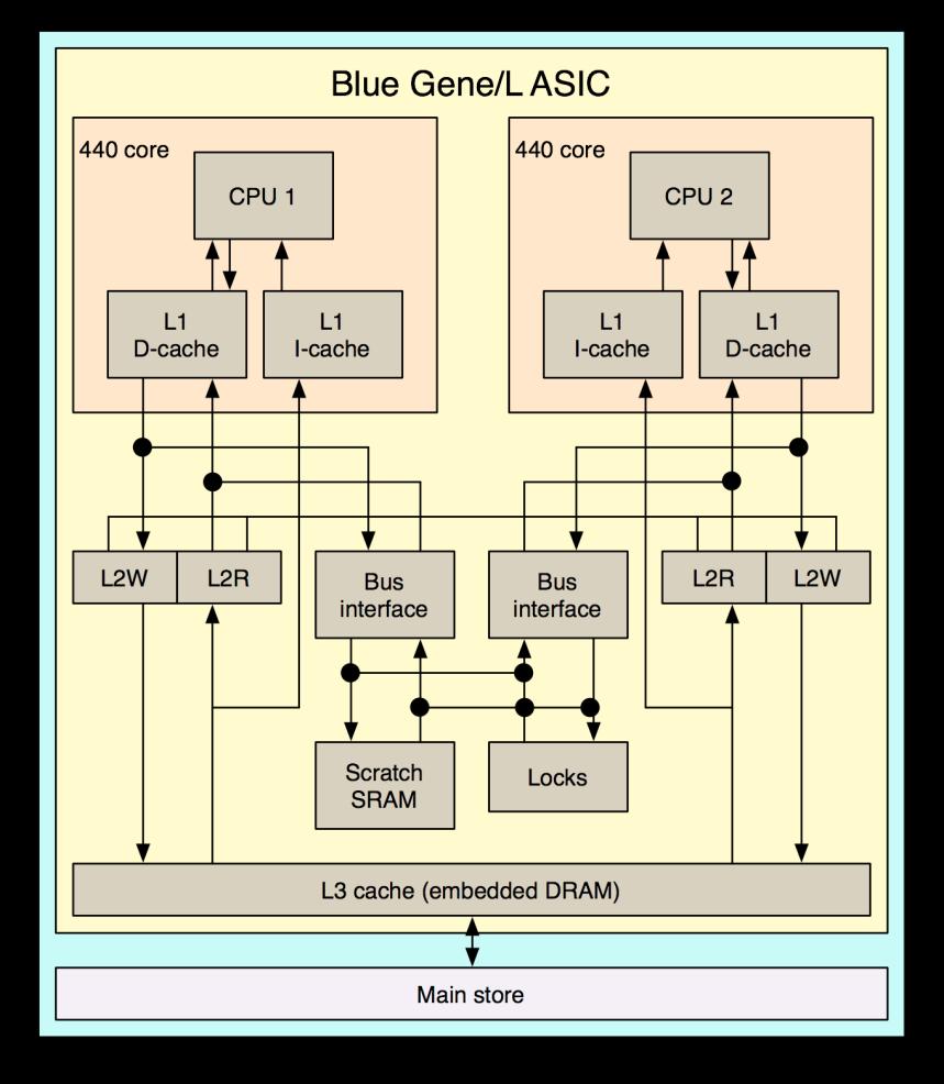
6 TREE DIAGRAM OF INTEGRATED CIRCUIT DESIGN METHODOLOGY 6
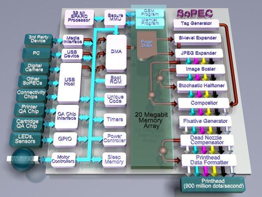
7 ASICs Application Specific Integrated Circuits. Definition : An integrated circuit (IC) customized for a particular use, rather than intended for general-purpose use. For example, a chip designed solely to run a cell phone is an ASIC. Why using ASIC? Higher reliability Faster turn-around time (total time taken between the submission of a program for execution and the return of the complete output to the costumer.) Tighter security Lower non-recurring cost (unusual charge, expense or lost that is unlikely to occur again in the normal course. Ex: design, development or loses. Also called extraordinary cost) Better performance 7

8 8

9 ADVANTAGES OF ASIC Fine-tuning refers to circumstances when the parameters of a model must be adjusted very precisely in order to agree with observation. 9

10 Specific costum IC VS Standard IC Multiple sourcing is the practice of buying in items from more than one source to reduce the risk of production or sales being disrupted from any problems that may take place in the supply chain. 10
11 LEARNING OUTCOMES 4.2 FULL-CUSTOM DESIGN By the end of this unit, student should be able to: 1. Explain the full-custom methodology for integrated circuit. 2. Explain the semi-custom methodology for integrated circuit. 3. Discuss the advantages and disadvantages of full-custom methodology. 4. Discuss the advantages and disadvantages of semicustom methodology. 11
12 DEFINITION Full-custom IC design is a methodology for designing integrated circuits by specifying the layout of each individual transistor and the interconnections between them. Full-custom IC design potentially maximizes the performance of the chip, and minimizes its area, but is extremely labor-intensive to implement. Full-custom IC design is limited to ICs that are to be fabricated in extremely high volumes, notably certain microprocessors and a small number of ASICs. Time taken to design IC is longer and slow. A full-custom IC includes some (possibly all) logic cells that are customized and all mask layers that are customized. Therefore, full-custom ICs are the most expensive to manufacture and to design. Example : microprocessor. 12
13 DEFINITION Semi-custom IC design is a methodology for making an integrated circuit which a portion of the circuit function is predefined and unalterable, while other portions can be configured to meet the designer's specific needs. Designers have the capability of designing application-specific circuits themselves, using either standard cell libraries or preconfigured arrays. In semicustom IC, all of the logic cells are predesigned and some (possibly all) of the mask layers are customized. Using predesigned cells from a cell library makes our lives as designers much easier and faster. Therefore, semi-custom ICs are the less expensive to manufacture and to design. Examples : ethernet chip, hard disk controller 13
14 FULL-CUSTOM IC DESIGN ADVANTAGES 1. substantial reduction in die (chip) area. 2. Ability to integrate analog component and pre-designed components. 3. High degree of optimization in performance and area. DISADVANTAGES 1. Increase design time. 2. Large amount of design expense and effort. 3. Complexity and highest risk. SEMI-CUSTOM IC DESIGN ADVANTAGES 1. rapid turn around. 2. design is performed at the logic gate level. 3. simplified verification. DISADVANTAGES 14
15 LEARNING OUTCOMES 4.3 SEMI-CUSTOM DESIGN By the end of this unit, student should be able to: 1. Explain the gate-array methodology. 2. State and draw the basic elements in CMOS gate-array. 3. Discuss the advantages and disadvantages of gate-array methodology. 4. Discuss two (2) methods to increase the percentage of gate used. 15
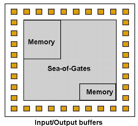
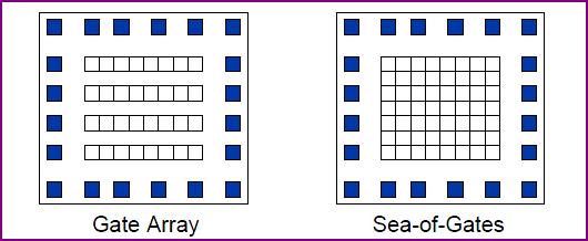
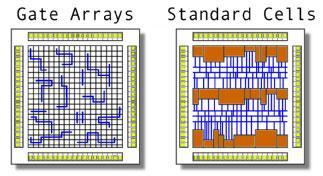
16 DEFINITION A gate array or uncommitted logic array (ULA) is an approach to the design and manufacture of application-specific integrated circuits (ASICs). A gate array circuit is a prefabricated silicon chip circuit with no particular function in which transistors, standard NAND or NOR logic gates, and other active devices are placed at regular predefined positions and manufactured on a wafer. Parts of the chip (transistors) are pre-fabricated, and other parts (wires) are custom fabricated for a particular customer s circuit. accomplished by adding layers of metal interconnects to the chips. Two types of gate array: Traditional (channeled) Gate Array Sea-of-Gate Gate Array - the routing is performed over the gates, hence more metal layers required, but the gate density is much higher than in a channel gate array. 16
17 17
18 18
19 19
20 ADVANTAGES GATE ARRAY 1. Low Cost Gate Arrays can be purchased for less than a dollar per unit. And for a given process, they can be packaged smaller than FPGAs, thereby reducing the circuit area and contributing to a reduction of total cost. 2. Stabilization of component procurement (perolehan) Gate Array is a custom product, and can hence be delivered in stable quantities based on your demand forecast information. 3. Security With Gate Arrays, the customer s proprietary circuit design is hard-wired onto the semi-custom ICs, making it impossible to duplicate. When using FPGA, the customer's proprietary circuit data is stored on a ROM, and FPGA is a general-purpose product. Hence, the circuit data can be intercepted and duplicated by monitoring the bit stream between the ROM and the FPGA during start-up. DISADVANTAGES 1. performance not as good as full-custom or standardcell-based ICs. 2. Non optimizing spacing and excess circuitry. 3. Limited transistor sizing options in terms of density, performance and power. 4. shorter manufacture lead time 4. Wiring blockage and inefficiences 20
21 GATE ARRAY Two (2) methods to increase the percentage of gate used: Using the same design. Using sea-of-gate rather than channelled gate array. 21
22 LEARNING OUTCOMES 4.3 SEMI-CUSTOM DESIGN By the end of this unit, student should be able to: 1. Explain the standard cells methodology. 2. Draw a design layout of standard cells. 3. Discuss the advantages and disadvantages of standard cells methodology. 22
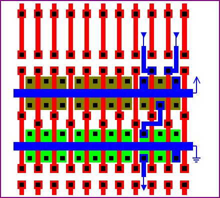
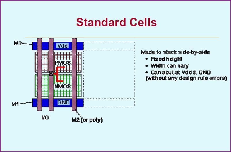
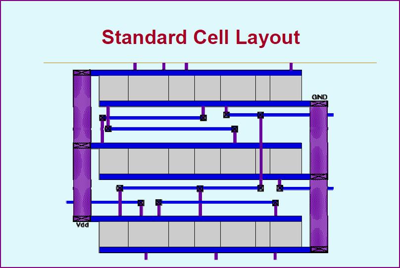
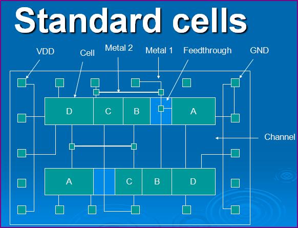
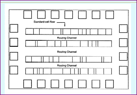
23 DEFINITION Standard Cell methodology is a method of designing applicationspecific integrated circuits (ASICs) with mostly digital-logic features. Standard cell methodology is an example of design abstraction, whereby a low-level very-large-scale integration (VLSI) layout is encapsulated into an abstract logic representation (such as a NAND gate) Standard Cell is a group of transistor and interconnect structures that provides a Boolean Logic function (e.g., AND, OR, XOR, XNOR, inverters) or a storage function (flipflop or latch). The simplest cells are direct representations of the elemental NAND, NOR, and XOR boolean function. Two types: Channelled Cells Channel-less Cells 23
24 24
25 25
26 26
27 27
28 28
29 29
30 STANDARD CELLS ADVANTAGES 1. More flexible to include digital as well as analog functions. 2. More compact design (less routing area, improved speed) 3. More sophisticated systems can be built (using parameterized cells, microprocessors) Parameterized: n-bit counters, shift registers, PLAs, RAMs, ROMs. DISADVANTAGES 1. Costs in additional mask-making, software, and workstation resources 2. Wasted chip area will be high due to the area occupied by the wiring channels can exceed 50% of the internal chip. This problem can be greatly reduced by using multiple metal layers in chip designs. 3. No saving in fabrication time due to no prefabricated cells. 30
31 LEARNING OUTCOMES 4.3 SELECTION CRITERIA By the end of this unit, student should be able to: 1. State the design methodology selection criteria. 2. Compare the design methodologies based on the criteria in 1. 31
32 Design Methodology Selection Criteria The choice of design style depends on the of the chip, and to be manufactured. Full custom design is used for and other. While FPGA may be used for simple and low volume applications. For large circuits, it is common to partition the circuit into smaller subcircuits which are designed using different team. 32 Each team may use different design.
33 33
34 Comparison of Design Styles Full-Custom Standard Cell Gate Array FPGA Cell size variable fixed height fixed fixed Cell type variable variable fixed programma ble Cell placement variable in row fixed fixed Interconnections variable variable variable programma ble Fabrication layers all layers all layers routing layers only no layers 34
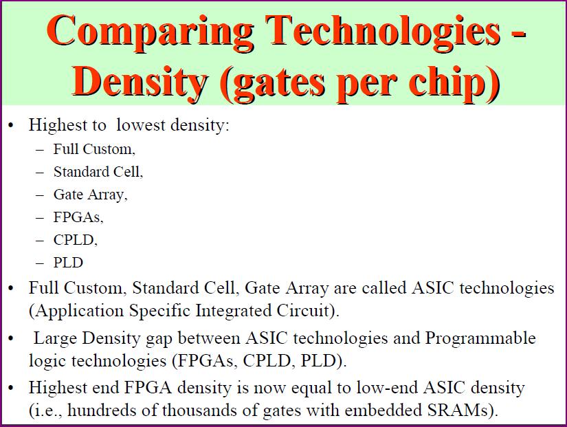
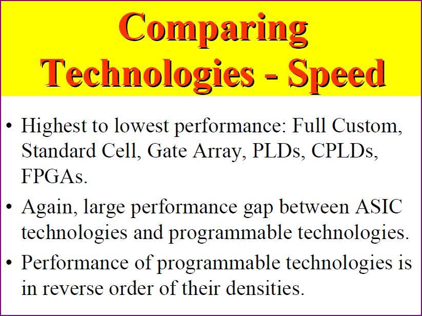
35 Comparison of Design Styles Full-Custom Standard Cell Gate Array FPGA Area compact compact to moderate moderate large Performance high high to moderate moderate low Design cost high medium medium low Time-to-market long medium medium short 35
36 SOURCE Prof. David Pan Office: ACES 5.434
37 37
38 38
39 39
40 40
41 41
42 42
Chapter 5: ASICs Vs. PLDs
 Chapter 5: ASICs Vs. PLDs 5.1 Introduction A general definition of the term Application Specific Integrated Circuit (ASIC) is virtually every type of chip that is designed to perform a dedicated task.
Design Methodologies. Full-Custom Design
 Design Methodologies Design styles Full-custom design Standard-cell design Programmable logic Gate arrays and field-programmable gate arrays (FPGAs) Sea of gates System-on-a-chip (embedded cores) Design
Digital Electronics 27. Digital System Design using PLDs
 1 Module -27 Digital System Design 1. Introduction 2. Digital System Design 2.1 Standard (Fixed function) ICs based approach 2.2 Programmable ICs based approach 3. Comparison of Digital System Design approaches
Design Methodologies and Tools. Full-Custom Design
 Design Methodologies and Tools Design styles Full-custom design Standard-cell design Programmable logic Gate arrays and field-programmable gate arrays (FPGAs) Sea of gates System-on-a-chip (embedded cores)
DIGITAL DESIGN TECHNOLOGY & TECHNIQUES
 DIGITAL DESIGN TECHNOLOGY & TECHNIQUES CAD for ASIC Design 1 INTEGRATED CIRCUITS (IC) An integrated circuit (IC) consists complex electronic circuitries and their interconnections. William Shockley et
Digital Design Methodology
 Digital Design Methodology Prof. Soo-Ik Chae Digital System Designs and Practices Using Verilog HDL and FPGAs @ 2008, John Wiley 1-1 Digital Design Methodology (Added) Design Methodology Design Specification
Spiral 2-8. Cell Layout
 2-8.1 Spiral 2-8 Cell Layout 2-8.2 Learning Outcomes I understand how a digital circuit is composed of layers of materials forming transistors and wires I understand how each layer is expressed as geometric
CS310 Embedded Computer Systems. Maeng
 1 INTRODUCTION (PART II) Maeng Three key embedded system technologies 2 Technology A manner of accomplishing a task, especially using technical processes, methods, or knowledge Three key technologies for
Digital Design Methodology (Revisited) Design Methodology: Big Picture
 Design Methodology: Big Picture") Digital Design Methodology (Revisited) Design Methodology Design Specification Verification Synthesis Technology Options Full Custom VLSI Standard Cell ASIC FPGA CS 150 Fall 2005 - Lec #25 Design Methodology
Digital Design Methodology (Revisited) Design Methodology Design Specification Verification Synthesis Technology Options Full Custom VLSI Standard Cell ASIC FPGA CS 150 Fall 2005 - Lec #25 Design Methodology
! Memory Overview. ! ROM Memories. ! RAM Memory " SRAM " DRAM. ! This is done because we can build. " large, slow memories OR
 ESE 57: Digital Integrated Circuits and VLSI Fundamentals Lec 2: April 5, 26 Memory Overview, Memory Core Cells Lecture Outline! Memory Overview! ROM Memories! RAM Memory " SRAM " DRAM 2 Memory Overview
COE 561 Digital System Design & Synthesis Introduction
 1 COE 561 Digital System Design & Synthesis Introduction Dr. Aiman H. El-Maleh Computer Engineering Department King Fahd University of Petroleum & Minerals Outline Course Topics Microelectronics Design
Hardware Design with VHDL PLDs I ECE 443. FPGAs can be configured at least once, many are reprogrammable.
 PLDs, ASICs and FPGAs FPGA definition: Digital integrated circuit that contains configurable blocks of logic and configurable interconnects between these blocks. Key points: Manufacturer does NOT determine
FPGA. Logic Block. Plessey FPGA: basic building block here is 2-input NAND gate which is connected to each other to implement desired function.
 FPGA Logic block of an FPGA can be configured in such a way that it can provide functionality as simple as that of transistor or as complex as that of a microprocessor. It can used to implement different
More Course Information
 More Course Information Labs and lectures are both important Labs: cover more on hands-on design/tool/flow issues Lectures: important in terms of basic concepts and fundamentals Do well in labs Do well
Hardware Design Environments. Dr. Mahdi Abbasi Computer Engineering Department Bu-Ali Sina University
 Hardware Design Environments Dr. Mahdi Abbasi Computer Engineering Department Bu-Ali Sina University Outline Welcome to COE 405 Digital System Design Design Domains and Levels of Abstractions Synthesis
Semiconductor Memory Classification. Today. ESE 570: Digital Integrated Circuits and VLSI Fundamentals. CPU Memory Hierarchy.
 ESE 57: Digital Integrated Circuits and VLSI Fundamentals Lec : April 4, 7 Memory Overview, Memory Core Cells Today! Memory " Classification " ROM Memories " RAM Memory " Architecture " Memory core " SRAM
UNIT IV CMOS TESTING
 UNIT IV CMOS TESTING 1. Mention the levels at which testing of a chip can be done? At the wafer level At the packaged-chip level At the board level At the system level In the field 2. What is meant by
CMPE 415 Programmable Logic Devices FPGA Technology I
 Department of Computer Science and Electrical Engineering CMPE 415 Programmable Logic Devices FPGA Technology I Prof. Ryan Robucci Some slides (blue-frame) developed by Jim Plusquellic Some images credited
FPGA for Dummies. Introduc)on to Programmable Logic
on to Programmable Logic") FPGA for Dummies Introduc)on to Programmable Logic FPGA for Dummies Historical introduc)on, where we come from; FPGA Architecture: Ø basic blocks (Logic, FFs, wires and IOs); Ø addi)onal elements; FPGA
FPGA for Dummies Introduc)on to Programmable Logic FPGA for Dummies Historical introduc)on, where we come from; FPGA Architecture: Ø basic blocks (Logic, FFs, wires and IOs); Ø addi)onal elements; FPGA
Lab. Course Goals. Topics. What is VLSI design? What is an integrated circuit? VLSI Design Cycle. VLSI Design Automation
 Course Goals Lab Understand key components in VLSI designs Become familiar with design tools (Cadence) Understand design flows Understand behavioral, structural, and physical specifications Be able to
Computer-Based Project on VLSI Design Co 3/7
 Computer-Based Project on VLSI Design Co 3/7 IC Layout and Symbolic Representation This pamphlet introduces the topic of IC layout in integrated circuit design and discusses the role of Design Rules and
Using ASIC circuits. What is ASIC. ASIC examples ASIC types and selection ASIC costs ASIC purchasing Trends in IC technologies
 Using ASIC circuits What is this machine? ASIC examples ASIC types and selection ASIC ASIC purchasing Trends in IC technologies 9.3.2004 Turo Piila 1 9.3.2004 Turo Piila 2 What is ASIC Floorplan and layout
Very Large Scale Integration (VLSI)
") Very Large Scale Integration (VLSI) Lecture 10 Dr. Ahmed H. Madian Ah_madian@hotmail.com Dr. Ahmed H. Madian-VLSI 1 Content Manufacturing Defects Wafer defects Chip defects Board defects system defects
Very Large Scale Integration (VLSI) Lecture 10 Dr. Ahmed H. Madian Ah_madian@hotmail.com Dr. Ahmed H. Madian-VLSI 1 Content Manufacturing Defects Wafer defects Chip defects Board defects system defects
LSN 6 Programmable Logic Devices
 LSN 6 Programmable Logic Devices Department of Engineering Technology LSN 6 What Are PLDs? Functionless devices in base form Require programming to operate The logic function of the device is programmed
INTRODUCTION TO FPGA ARCHITECTURE
 3/3/25 INTRODUCTION TO FPGA ARCHITECTURE DIGITAL LOGIC DESIGN (BASIC TECHNIQUES) a b a y 2input Black Box y b Functional Schematic a b y a b y a b y 2 Truth Table (AND) Truth Table (OR) Truth Table (XOR)
Programmable Logic Devices Introduction CMPE 415. Programmable Logic Devices
 Instructor: Professor Jim Plusquellic Programmable Logic Devices Text: The Design Warrior s Guide to FPGAs, Devices, Tools and Flows, Clive "Max" Maxfield, ISBN: 0-7506-7604-3 Modeling, Synthesis and Rapid
INTERCONNECT TESTING WITH BOUNDARY SCAN
 INTERCONNECT TESTING WITH BOUNDARY SCAN Paul Wagner Honeywell, Inc. Solid State Electronics Division 12001 State Highway 55 Plymouth, Minnesota 55441 Abstract Boundary scan is a structured design technique
Design Tools for 100,000 Gate Programmable Logic Devices
 esign Tools for 100,000 Gate Programmable Logic evices March 1996, ver. 1 Product Information Bulletin 22 Introduction The capacity of programmable logic devices (PLs) has risen dramatically to meet the
A VARIETY OF ICS ARE POSSIBLE DESIGNING FPGAS & ASICS. APPLICATIONS MAY USE STANDARD ICs or FPGAs/ASICs FAB FOUNDRIES COST BILLIONS
 architecture behavior of control is if left_paddle then n_state
CONTENTS CHAPTER 1: NUMBER SYSTEM. Foreword...(vii) Preface... (ix) Acknowledgement... (xi) About the Author...(xxiii)
 Preface... (ix) Acknowledgement... (xi) About the Author...(xxiii)") CONTENTS Foreword...(vii) Preface... (ix) Acknowledgement... (xi) About the Author...(xxiii) CHAPTER 1: NUMBER SYSTEM 1.1 Digital Electronics... 1 1.1.1 Introduction... 1 1.1.2 Advantages of Digital Systems...
CONTENTS Foreword...(vii) Preface... (ix) Acknowledgement... (xi) About the Author...(xxiii) CHAPTER 1: NUMBER SYSTEM 1.1 Digital Electronics... 1 1.1.1 Introduction... 1 1.1.2 Advantages of Digital Systems...
Enabling Intelligent Digital Power IC Solutions with Anti-Fuse-Based 1T-OTP
 Enabling Intelligent Digital Power IC Solutions with Anti-Fuse-Based 1T-OTP Jim Lipman, Sidense David New, Powervation 1 THE NEED FOR POWER MANAGEMENT SOLUTIONS WITH OTP MEMORY As electronic systems gain
EECS150 - Digital Design Lecture 6 - Field Programmable Gate Arrays (FPGAs)
") EECS150 - Digital Design Lecture 6 - Field Programmable Gate Arrays (FPGAs) September 12, 2002 John Wawrzynek Fall 2002 EECS150 - Lec06-FPGA Page 1 Outline What are FPGAs? Why use FPGAs (a short history
EECS150 - Digital Design Lecture 6 - Field Programmable Gate Arrays (FPGAs) September 12, 2002 John Wawrzynek Fall 2002 EECS150 - Lec06-FPGA Page 1 Outline What are FPGAs? Why use FPGAs (a short history
CHAPTER 12 ARRAY SUBSYSTEMS [ ] MANJARI S. KULKARNI
![CHAPTER 12 ARRAY SUBSYSTEMS [ ] MANJARI S. KULKARNI](/thumbs/76/73997056.jpg "CHAPTER 12 ARRAY SUBSYSTEMS [ ] MANJARI S. KULKARNI") CHAPTER 2 ARRAY SUBSYSTEMS [2.4-2.9] MANJARI S. KULKARNI OVERVIEW Array classification Non volatile memory Design and Layout Read-Only Memory (ROM) Pseudo nmos and NAND ROMs Programmable ROMS PROMS, EPROMs,
CHAPTER 2 ARRAY SUBSYSTEMS [2.4-2.9] MANJARI S. KULKARNI OVERVIEW Array classification Non volatile memory Design and Layout Read-Only Memory (ROM) Pseudo nmos and NAND ROMs Programmable ROMS PROMS, EPROMs,
CAD for VLSI. Debdeep Mukhopadhyay IIT Madras
 CAD for VLSI Debdeep Mukhopadhyay IIT Madras Tentative Syllabus Overall perspective of VLSI Design MOS switch and CMOS, MOS based logic design, the CMOS logic styles, Pass Transistors Introduction to Verilog
Outline. EECS150 - Digital Design Lecture 6 - Field Programmable Gate Arrays (FPGAs) FPGA Overview. Why FPGAs?
 FPGA Overview. Why FPGAs?") EECS150 - Digital Design Lecture 6 - Field Programmable Gate Arrays (FPGAs) September 12, 2002 John Wawrzynek Outline What are FPGAs? Why use FPGAs (a short history lesson). FPGA variations Internal logic
EECS150 - Digital Design Lecture 6 - Field Programmable Gate Arrays (FPGAs) September 12, 2002 John Wawrzynek Outline What are FPGAs? Why use FPGAs (a short history lesson). FPGA variations Internal logic
Semiconductor Memory Classification
 ESE37: Circuit-Level Modeling, Design, and Optimization for Digital Systems Lec 6: November, 7 Memory Overview Today! Memory " Classification " Architecture " Memory core " Periphery (time permitting)!
ECE 1160/2160 Embedded Systems Design. Midterm Review. Wei Gao. ECE 1160/2160 Embedded Systems Design
 ECE 1160/2160 Embedded Systems Design Midterm Review Wei Gao ECE 1160/2160 Embedded Systems Design 1 Midterm Exam When: next Monday (10/16) 4:30-5:45pm Where: Benedum G26 15% of your final grade What about:
Analog ASICs in industrial applications
 Analog ASICs in industrial applications Customised IC solutions for sensor interface applications in industrial electronics the requirements and the possibilities Synopsis Industrial electronics creates
Topics. ! PLAs.! Memories: ! Datapaths.! Floor Planning ! ROM;! SRAM;! DRAM. Modern VLSI Design 2e: Chapter 6. Copyright 1994, 1998 Prentice Hall
 Topics! PLAs.! Memories:! ROM;! SRAM;! DRAM.! Datapaths.! Floor Planning Programmable logic array (PLA)! Used to implement specialized logic functions.! A PLA decodes only some addresses (input values);
CHAPTER 1 INTRODUCTION
 CHAPTER 1 INTRODUCTION Rapid advances in integrated circuit technology have made it possible to fabricate digital circuits with large number of devices on a single chip. The advantages of integrated circuits
Design Methodologies
 Design Methodologies 1981 1983 1985 1987 1989 1991 1993 1995 1997 1999 2001 2003 2005 2007 2009 Complexity Productivity (K) Trans./Staff - Mo. Productivity Trends Logic Transistor per Chip (M) 10,000 0.1
High-Voltage Structured ASICs for Industrial Applications - A Single Chip Solution
 High-Voltage Structured ASICs for Industrial Applications - A Single Chip Solution Yipin Zhang, Cor Scherjon Institut für Mikroelektronik Stuttgart Allmandring 30 a 70569 Stuttgart This paper presents
Course Batch Semester Subject Code Subject Name. B.E-Marine Engineering B.E- ME-16 III UBEE307 Integrated Circuits
 Course Batch Semester Subject Code Subject Name B.E-Marine Engineering B.E- ME-16 III UBEE307 Integrated Circuits Part-A 1 Define De-Morgan's theorem. 2 Convert the following hexadecimal number to decimal
Digital Integrated Circuits
 Digital Integrated Circuits Lecture 9 Jaeyong Chung Robust Systems Laboratory Incheon National University DIGITAL DESIGN FLOW Chung EPC6055 2 FPGA vs. ASIC FPGA (A programmable Logic Device) Faster time-to-market
Actel s SX Family of FPGAs: A New Architecture for High-Performance Designs
 Actel s SX Family of FPGAs: A New Architecture for High-Performance Designs A Technology Backgrounder Actel Corporation 955 East Arques Avenue Sunnyvale, California 94086 April 20, 1998 Page 2 Actel Corporation
Integrated circuits and fabrication
 Integrated circuits and fabrication Motivation So far we have discussed about the various devices that are the heartbeat of core electronics. This modules aims at giving an overview of how these solid
Overview. CSE372 Digital Systems Organization and Design Lab. Hardware CAD. Two Types of Chips
 Overview CSE372 Digital Systems Organization and Design Lab Prof. Milo Martin Unit 5: Hardware Synthesis CAD (Computer Aided Design) Use computers to design computers Virtuous cycle Architectural-level,
Hardware Design with VHDL PLDs IV ECE 443
 Embedded Processor Cores (Hard and Soft) Electronic design can be realized in hardware (logic gates/registers) or software (instructions executed on a microprocessor). The trade-off is determined by how
Introduction to SRAM. Jasur Hanbaba
 Introduction to SRAM Jasur Hanbaba Outline Memory Arrays SRAM Architecture SRAM Cell Decoders Column Circuitry Non-volatile Memory Manufacturing Flow Memory Arrays Memory Arrays Random Access Memory Serial
OPERATIONAL UP TO. 300 c. Microcontrollers Memories Logic
 OPERATIONAL UP TO 300 c Microcontrollers Memories Logic Whether You Need an ASIC, Mixed Signal, Processor, or Peripheral, Tekmos is Your Source for High Temperature Electronics Using either a bulk silicon
Memory & Logic Array. Lecture # 23 & 24 By : Ali Mustafa
 Memory & Logic Array Lecture # 23 & 24 By : Ali Mustafa Memory Memory unit is a device to which a binary information is transferred for storage. From which information is retrieved when needed. Types of
FPGA for Complex System Implementation. National Chiao Tung University Chun-Jen Tsai 04/14/2011
 FPGA for Complex System Implementation National Chiao Tung University Chun-Jen Tsai 04/14/2011 About FPGA FPGA was invented by Ross Freeman in 1989 SRAM-based FPGA properties Standard parts Allowing multi-level
EEL 4783: HDL in Digital System Design
 EEL 4783: HDL in Digital System Design Lecture 13: Floorplanning Prof. Mingjie Lin Topics Partitioning a design with a floorplan. Performance improvements by constraining the critical path. Floorplanning
Introduction. Sungho Kang. Yonsei University
 Introduction Sungho Kang Yonsei University Outline VLSI Design Styles Overview of Optimal Logic Synthesis Model Graph Algorithm and Complexity Asymptotic Complexity Brief Summary of MOS Device Behavior
TABLE OF CONTENTS III. Section 1. Executive Summary
 Section 1. Executive Summary... 1-1 Section 2. Global IC Industry Outlook and Cycles... 2-1 IC Insights' Forecast Methodology... 2-1 Overview... 2-1 Worldwide GDP... 2-1 Electronic System Sales... 2-2
101-1 Under-Graduate Project Digital IC Design Flow
 101-1 Under-Graduate Project Digital IC Design Flow Speaker: Ming-Chun Hsiao Adviser: Prof. An-Yeu Wu Date: 2012/9/25 ACCESS IC LAB Outline Introduction to Integrated Circuit IC Design Flow Verilog HDL
Graphics: Alexandra Nolte, Gesine Marwedel, Universität Dortmund. RTL Synthesis
 Graphics: Alexandra Nolte, Gesine Marwedel, 2003 Universität Dortmund RTL Synthesis Purpose of HDLs Purpose of Hardware Description Languages: Capture design in Register Transfer Language form i.e. All
ESE370: Circuit-Level Modeling, Design, and Optimization for Digital Systems
 ESE370: Circuit-Level Modeling, Design, and Optimization for Digital Systems Lec 26: November 9, 2018 Memory Overview Dynamic OR4! Precharge time?! Driving input " With R 0 /2 inverter! Driving inverter
ESE 570 Cadence Lab Assignment 2: Introduction to Spectre, Manual Layout Drawing and Post Layout Simulation (PLS)
") ESE 570 Cadence Lab Assignment 2: Introduction to Spectre, Manual Layout Drawing and Post Layout Simulation (PLS) Objective Part A: To become acquainted with Spectre (or HSpice) by simulating an inverter,
ESE 570 Cadence Lab Assignment 2: Introduction to Spectre, Manual Layout Drawing and Post Layout Simulation (PLS) Objective Part A: To become acquainted with Spectre (or HSpice) by simulating an inverter,
ECE520 VLSI Design. Lecture 1: Introduction to VLSI Technology. Payman Zarkesh-Ha
 ECE520 VLSI Design Lecture 1: Introduction to VLSI Technology Payman Zarkesh-Ha Office: ECE Bldg. 230B Office hours: Wednesday 2:00-3:00PM or by appointment E-mail: pzarkesh@unm.edu Slide: 1 Course Objectives
Selecting PLLs for ASIC Applications Requires Tradeoffs
 Selecting PLLs for ASIC Applications Requires Tradeoffs John G. Maneatis, Ph.., President, True Circuits, Inc. Los Altos, California October 7, 2004 Phase-Locked Loops (PLLs) are commonly used to perform
Memory Systems IRAM. Principle of IRAM
 Memory Systems 165 other devices of the module will be in the Standby state (which is the primary state of all RDRAM devices) or another state with low-power consumption. The RDRAM devices provide several
UNIT V (PROGRAMMABLE LOGIC DEVICES)
") UNIT V (PROGRAMMABLE LOGIC DEVICES) Introduction There are two types of memories that are used in digital systems: Random-access memory(ram): perform both the write and read operations. Read-only memory(rom):
UNIT V (PROGRAMMABLE LOGIC DEVICES) Introduction There are two types of memories that are used in digital systems: Random-access memory(ram): perform both the write and read operations. Read-only memory(rom):
Programmable Logic Devices II
 São José February 2015 Prof. Hoeller, Prof. Moecke (http://www.sj.ifsc.edu.br) 1 / 28 Lecture 01: Complexity Management and the Design of Complex Digital Systems Prof. Arliones Hoeller arliones.hoeller@ifsc.edu.br
Digital Integrated Circuits A Design Perspective. Jan M. Rabaey
 Digital Integrated Circuits A Design Perspective Jan M. Rabaey Outline (approximate) Introduction and Motivation The VLSI Design Process Details of the MOS Transistor Device Fabrication Design Rules CMOS
This presentation will..
 Component Identification: Digital Introduction to Logic Gates and Integrated Circuits Digital Electronics 2014 This presentation will.. Introduce transistors, logic gates, integrated circuits (ICs), and
Intro to Logic Gates & Datasheets. Digital Electronics
 Intro to Logic Gates & Datasheets Digital Electronics Intro to Logic Gates & Datasheets This presentation will Introduce integrated circuits (ICs). Present an overview of : Transistor-Transistor Logic
Unit 6 1.Random Access Memory (RAM) Chapter 3 Combinational Logic Design 2.Programmable Logic
 Chapter 3 Combinational Logic Design 2.Programmable Logic") EE 200: Digital Logic Circuit Design Dr Radwan E Abdel-Aal, COE Unit 6.Random Access Memory (RAM) Chapter 3 Combinational Logic Design 2. Logic Logic and Computer Design Fundamentals Part Implementation
EE 200: Digital Logic Circuit Design Dr Radwan E Abdel-Aal, COE Unit 6.Random Access Memory (RAM) Chapter 3 Combinational Logic Design 2. Logic Logic and Computer Design Fundamentals Part Implementation
Intro to Logic Gates & Datasheets. Intro to Logic Gates & Datasheets. Introduction to Integrated Circuits. TTL Vs. CMOS Logic
 Intro to Logic Gates & Datasheets Digital Electronics Intro to Logic Gates & Datasheets This presentation will Introduce integrated circuits (ICs). Present an overview of : Transistor-Transistor Logic
Memory and Programmable Logic
 Memory and Programmable Logic Memory units allow us to store and/or retrieve information Essentially look-up tables Good for storing data, not for function implementation Programmable logic device (PLD),
3D systems-on-chip. A clever partitioning of circuits to improve area, cost, power and performance. The 3D technology landscape
 Edition April 2017 Semiconductor technology & processing 3D systems-on-chip A clever partitioning of circuits to improve area, cost, power and performance. In recent years, the technology of 3D integration
Today. Comments about assignment Max 1/T (skew = 0) Max clock skew? Comments about assignment 3 ASICs and Programmable logic Others courses
 Max clock skew? Comments about assignment 3 ASICs and Programmable logic Others courses") Today Comments about assignment 3-43 Comments about assignment 3 ASICs and Programmable logic Others courses octor Per should show up in the end of the lecture Mealy machines can not be coded in a single
Today Comments about assignment 3-43 Comments about assignment 3 ASICs and Programmable logic Others courses octor Per should show up in the end of the lecture Mealy machines can not be coded in a single
VLSI Design Automation
 VLSI Design Automation IC Products Processors CPU, DSP, Controllers Memory chips RAM, ROM, EEPROM Analog Mobile communication, audio/video processing Programmable PLA, FPGA Embedded systems Used in cars,
Introduction to ICs and Transistor Fundamentals
 Introduction to ICs and Transistor Fundamentals A Brief History 1958: First integrated circuit Flip-flop using two transistors Built by Jack Kilby at Texas Instruments 2003 Intel Pentium 4 mprocessor (55
ASIC, Customer-Owned Tooling, and Processor Design
 ASIC, Customer-Owned Tooling, and Processor Design Design Style Myths That Lead EDA Astray Nancy Nettleton Manager, VLSI ASIC Device Engineering April 2000 Design Style Myths COT is a design style that
ADVANCED FPGA BASED SYSTEM DESIGN. Dr. Tayab Din Memon Lecture 3 & 4
 ADVANCED FPGA BASED SYSTEM DESIGN Dr. Tayab Din Memon tayabuddin.memon@faculty.muet.edu.pk Lecture 3 & 4 Books Recommended Books: Text Book: FPGA Based System Design by Wayne Wolf Overview Why VLSI? Moore
Control System Implementation
 Control System Implementation Hardware implementation Electronic Control systems are also: Members of the Mechatronic Systems Concurrent design (Top-down approach?) Mechanic compatibility Solve the actual
PLAs & PALs. Programmable Logic Devices (PLDs) PLAs and PALs
 PLAs and PALs") PLAs & PALs Programmable Logic Devices (PLDs) PLAs and PALs PLAs&PALs By the late 1970s, standard logic devices were all the rage, and printed circuit boards were loaded with them. To offer the ultimate
PLAs & PALs Programmable Logic Devices (PLDs) PLAs and PALs PLAs&PALs By the late 1970s, standard logic devices were all the rage, and printed circuit boards were loaded with them. To offer the ultimate
FPGA Power Management and Modeling Techniques
 FPGA Power Management and Modeling Techniques WP-01044-2.0 White Paper This white paper discusses the major challenges associated with accurately predicting power consumption in FPGAs, namely, obtaining
DIGITAL SYSTEM FUNDAMENTALS (ECE421) DIGITAL ELECTRONICS FUNDAMENTAL (ECE4220. PROGRAMMABLE LOGIC DEVICES (PLDs)
 DIGITAL ELECTRONICS FUNDAMENTAL (ECE4220. PROGRAMMABLE LOGIC DEVICES (PLDs)") COURSE / CODE DIGITAL SYSTEM FUNDAMENTALS (ECE421) DIGITAL ELECTRONICS FUNDAMENTAL (ECE4220 PROGRAMMABLE LOGIC DEVICES (PLDs) A PLD, or programmable logic device, is an electronic component that is used
COURSE / CODE DIGITAL SYSTEM FUNDAMENTALS (ECE421) DIGITAL ELECTRONICS FUNDAMENTAL (ECE4220 PROGRAMMABLE LOGIC DEVICES (PLDs) A PLD, or programmable logic device, is an electronic component that is used
RETI LOGICHE. Sito del corso:
 RETI LOGICHE Sito del corso: http://vision.unipv.it/reti-logiche/ Design of Integrated Digital Systems System Level Register Transfer Level Gate Level Transistor Level Layout Level Mask Level 2 System
Section 6. Memory Components Chapter 5.7, 5.8 Physical Implementations Chapter 7 Programmable Processors Chapter 8
 Section 6 Memory Components Chapter 5.7, 5.8 Physical Implementations Chapter 7 Programmable Processors Chapter 8 Types of memory Two major types of memory Volatile When power to the device is removed
Moore s Law: Alive and Well. Mark Bohr Intel Senior Fellow
 Moore s Law: Alive and Well Mark Bohr Intel Senior Fellow Intel Scaling Trend 10 10000 1 1000 Micron 0.1 100 nm 0.01 22 nm 14 nm 10 nm 10 0.001 1 1970 1980 1990 2000 2010 2020 2030 Intel Scaling Trend
FPGA Based Digital Design Using Verilog HDL
 FPGA Based Digital Design Using Course Designed by: IRFAN FAISAL MIR ( Verilog / FPGA Designer ) irfanfaisalmir@yahoo.com * Organized by Electronics Division Integrated Circuits Uses for digital IC technology
Lecture 13: SRAM. Slides courtesy of Deming Chen. Slides based on the initial set from David Harris. 4th Ed.
 Lecture 13: SRAM Slides courtesy of Deming Chen Slides based on the initial set from David Harris CMOS VLSI Design Outline Memory Arrays SRAM Architecture SRAM Cell Decoders Column Circuitry Multiple Ports
Introduction 1. GENERAL TRENDS. 1. The technology scale down DEEP SUBMICRON CMOS DESIGN
 1 Introduction The evolution of integrated circuit (IC) fabrication techniques is a unique fact in the history of modern industry. The improvements in terms of speed, density and cost have kept constant
Lecture 3 Introduction to VHDL
 CPE 487: Digital System Design Spring 2018 Lecture 3 Introduction to VHDL Bryan Ackland Department of Electrical and Computer Engineering Stevens Institute of Technology Hoboken, NJ 07030 1 Managing Design
UNIT - V MEMORY P.VIDYA SAGAR ( ASSOCIATE PROFESSOR) Department of Electronics and Communication Engineering, VBIT
 Department of Electronics and Communication Engineering, VBIT") UNIT - V MEMORY P.VIDYA SAGAR ( ASSOCIATE PROFESSOR) contents Memory: Introduction, Random-Access memory, Memory decoding, ROM, Programmable Logic Array, Programmable Array Logic, Sequential programmable
UNIT - V MEMORY P.VIDYA SAGAR ( ASSOCIATE PROFESSOR) contents Memory: Introduction, Random-Access memory, Memory decoding, ROM, Programmable Logic Array, Programmable Array Logic, Sequential programmable
2 Introduction Chap. 1
 1 Introduction This book is devoted to the development of routing techniques to achieve minimum area layouts for very large scale integration (VLSI) systems. Minimum area layouts not only deliver the optimum
Lecture 11 SRAM Zhuo Feng. Z. Feng MTU EE4800 CMOS Digital IC Design & Analysis 2010
 EE4800 CMOS Digital IC Design & Analysis Lecture 11 SRAM Zhuo Feng 11.1 Memory Arrays SRAM Architecture SRAM Cell Decoders Column Circuitryit Multiple Ports Outline Serial Access Memories 11.2 Memory Arrays
END-TERM EXAMINATION
 (Please Write your Exam Roll No. immediately) END-TERM EXAMINATION DECEMBER 2006 Exam. Roll No... Exam Series code: 100919DEC06200963 Paper Code: MCA-103 Subject: Digital Electronics Time: 3 Hours Maximum
SECTION-A
 M.Sc(CS) ( First Semester) Examination,2013 Digital Electronics Paper: Fifth ------------------------------------------------------------------------------------- SECTION-A I) An electronics circuit/ device
PROGRAMMABLE LOGIC DEVICES
 PROGRAMMABLE LOGIC DEVICES Programmable logic devices (PLDs) are used for designing logic circuits. PLDs can be configured by the user to perform specific functions. The different types of PLDs available
ECE 3220 Digital Design with VHDL. Course Information. Lecture 1
 ECE 3220 Digital Design with VHDL Course Information Lecture 1 Course Information Course #: ECE 3220 Course Name: Digital Design with VHDL Course Instructor: Dr. Vida Vakilian Email: vvakilian@csub.edu
ECE 485/585 Microprocessor System Design
 Microprocessor System Design Lecture 4: Memory Hierarchy Memory Taxonomy SRAM Basics Memory Organization DRAM Basics Zeshan Chishti Electrical and Computer Engineering Dept Maseeh College of Engineering
William Stallings Computer Organization and Architecture 8th Edition. Chapter 5 Internal Memory
 William Stallings Computer Organization and Architecture 8th Edition Chapter 5 Internal Memory Semiconductor Memory The basic element of a semiconductor memory is the memory cell. Although a variety of
Enhanced Multi-Threshold (MTCMOS) Circuits Using Variable Well Bias
 Circuits Using Variable Well Bias") Bookmark file Enhanced Multi-Threshold (MTCMOS) Circuits Using Variable Well Bias Stephen V. Kosonocky, Mike Immediato, Peter Cottrell*, Terence Hook*, Randy Mann*, Jeff Brown* IBM T.J. Watson Research
Bookmark file Enhanced Multi-Threshold (MTCMOS) Circuits Using Variable Well Bias Stephen V. Kosonocky, Mike Immediato, Peter Cottrell*, Terence Hook*, Randy Mann*, Jeff Brown* IBM T.J. Watson Research
Sense Amplifiers 6 T Cell. M PC is the precharge transistor whose purpose is to force the latch to operate at the unstable point.
 Announcements (Crude) notes for switching speed example from lecture last week posted. Schedule Final Project demo with TAs. Written project report to include written evaluation section. Send me suggestions
Memories. Design of Digital Circuits 2017 Srdjan Capkun Onur Mutlu.
 Memories Design of Digital Circuits 2017 Srdjan Capkun Onur Mutlu http://www.syssec.ethz.ch/education/digitaltechnik_17 Adapted from Digital Design and Computer Architecture, David Money Harris & Sarah
ELCT 501: Digital System Design
 ELCT 501: Digital System Lecture 1: Introduction Dr. Mohamed Abd El Ghany, Mohamed.abdel-ghany@guc.edu.eg Administrative Rules Course components: Lecture: Thursday (fourth slot), 13:15-14:45 (H8) Office