Win-I2CUSB. Software User s Manual
|
|
|
- Curtis Hutchinson
- 6 years ago
- Views:
Transcription

1 Win-I2CUSB Software User s Manual
2 Information provided in this document is solely for use with Win-I2CUSB. The Boardshop and SB Solutions, Inc. reserve the right to make changes or improvements to this document at any time without notice. We assume no liability whatsoever in the sale or use of this product, including infringement of any patent or copyright. No part of this document may be reproduced or transmitted in any form or by any means, electronic or mechanical, for any purpose, without the express written permission of The Boardshop and SB Solutions, Inc. Microsoft and Windows are registered trademarks of Microsoft Corporation. Delphi and C++ Builder are trademarks of Embarcadero Technologies. Other brand names are trademarks or registered trademarks of their respective owners. Questions or comments regarding this document should be ed to The Boardshop / SB Solutions, Inc. All rights reserved. December 2010 Win-I2CUSB Software User s Manual Page 2
3 Win-I2CUSB Software User s Manual Page 3
4 I²C PROTOCOL... 9 GENERAL CHARACTERISTICS... 9 BIT TRANSFER... 9 START AND STOP CONDITIONS... 9 I²C ADDRESS... 9 I²C BUS DOCUMENTATION... 9 MAIN SCREEN Device Menu Message Panel Messages: File Menu Save Data Load Data Options Menu I²C Frequency Menu Item Enable 3.3V Output Power Enable 5V Output Power Ignore Acknowledge Windows Menu Frequency Indicator I²C Address Write Page Size Selection Erase/Write Cycle Time Data Grid Byte Address (Subaddress) Read Byte Button Read All Button Write Byte Button Write All Button Verify Button Fill Buffer Checkerboard Inverted Checkerboard Goto Byte Copy Block UNIVERSAL INTERFACES USER DEFINABLE DEVICE Define New Device Open Device Definition File Save Save As Save Registers in text format Byte Mode Print Device Data Data Grid Edit Menu Edit Current Register Edit Current Device Slider Control Spin Control Bit Control EXPERT MODE Open New Page Open Data File Save Data Close Expert Mode Add a Row Win-I2CUSB Software User s Manual Page 4
5 Delete a Row Clear the current row Copy the Current Row Paste Data Compress Data Send Message Send All Send Sequence Message Editor Message Number Delay after message Device Address Read/Write Selection Stop? Message Data GPIO Control IO EXPANDERS PCA9500/PCA BIT I2C I/O PORT WITH INTERRUPT AND 2K EEPROM Changing I/O Expander Data with Checkboxes Read I/O Button Set Data Word Address Read Byte Button Read All Button Write Byte Button Write All Button PCA9534/PCA9538/PCA9554/PCA9554A 8-BIT I/O EXPANDERS WITH INTERRUPT Automatic Write Enable Checkboxes Edit Boxes Read Buttons Write Button PCA9535/PCA9555/PCA BIT I/O EXPANDERS WITH INTERRUPT Input Registers (subaddress 0x00 and 0x01) Output Registers (subaddress 0x02 and 0x03) Polarity Registers (subaddress 0x04 and 0x05) Configuration Register (subaddress 0x06 and 0x07) Automatic Write Enable Checkboxes Edit Boxes Read Buttons PCA9556/PCA BIT I/O EXPANDER WITH RESET Auto Write Read All Button Write All Button Register 0 (Input Port) Register 1 (Output port) Register 2 (Polarity) Register 3 (Configuration) PCA9536/PCA BIT I/O EXPANDERS WITH RESET Auto Write Read All Button Write All Button Register 0 (Input Port) Register 1 (Output port) Register 2 (Polarity) Register 3 (Configuration) PCF8574/PCF8574A 8-BIT I/O EXPANDER Win-I2CUSB Software User s Manual Page 5
6 Checkboxes Read Button Read Data Data Byte Write Button Automatic Write Enable Auto Readback PCF BIT I/O EXPANDER Read Checkboxes Write Checkboxes Read Button Write Button Read Data Boxes Write Data Boxes Auto Write LED BLINKERS AND DIMMERS PCA BIT I2C LED DIMMER Device Address Auto Write On/Off Button LED Mode Selector PWM Period Slidebar PWM Duty Cycle Write All Button Read Input Register Read All Button PCA BIT I2C LED DIMMER Device Address Auto Write On/Off Button LED Mode Selector PWM Period Slidebar PWM Duty Cycle Write All Button Read Input Register Read All Button PCA BIT I2C LED DIMMER Device Address Auto Write On/Off Button LED Mode Selector PWM Period Slidebar PWM Duty Cycle Write All Button Read Input Register Read All Button PCA BIT I2C LED DIMMER Device Address Auto Write On/Off Button LED Mode Selector PWM Period Slidebar PWM Duty Cycle Write All Button Read Input Register Read All Button PCA BIT I2C LED BLINKER Device Address Auto Write On/Off Button LED Mode Selector PWM Period Slidebar PWM Duty Cycle Win-I2CUSB Software User s Manual Page 6
7 Write All Button Read Input Register Read All Button PCA BIT I2C LED BLINKER Device Address Auto Write On/Off Button LED Mode Selector PWM Period Slidebar PWM Duty Cycle Write All Button Read Input Register Read All Button PCA BIT I2C LED BLINKER Device Address Auto Write On/Off Button LED Mode Selector PWM Period Slidebar PWM Duty Cycle Write All Button Read Input Register Read All Button PCA BIT I2C LED BLINKER Device Address Auto Write On/Off Button LED Mode Selector PWM Period Slidebar PWM Duty Cycle Write All Button Read Input Register Read All Button SAA DIGIT LED-DRIVER Control Register Automatic Write Digits 1, 2, 3, and Instruction Byte Read Address Status Register Read Status Button Write Button TO-1 I2C MASTER SELECTOR PCA Register 0: Mask Register Register 1: Control Register Register 2: Interrupt Status Register MULTIPLEXER / SWITCHES PCA9540B/PCA9542A/PCA9544A/PCA Control Register Interrupts Multiplexer Control Auto Write PCA9543A/PCA9545A/PCA9546A/PCA9548A/PCA Control Register Interrupts Channel Selection Auto Write NON-VOLATILE REGISTERS Win-I2CUSB Software User s Manual Page 7
8 PCA8550/PCA9559/PCA9560/PCA Address Selection Data Register EEPROM Byte x MUX_OUT Auto Write THERMAL MANAGEMENT LM75A DIGITAL TEMPERATURE SENSOR AND THERMAL WATCHDOG Device Address Automatic Write (Checkbox) Write All Read All Temperature Register (Temp) Thyst (Hysteresis) Register TOS (Overtemp shut-down threshold) Register Configuration Register Start Read Button NE1617(A) TEMPERATURE MONITOR Read-Only Registers Write Only Registers Auto Write SA56004A TEMPERATURE MONITOR Read-Only Registers Write Only Registers Read/Write Registers Auto Write Cyclic Read SE98 TEMPERATURE MONITOR Read-Only Registers Read/Write Registers Auto Write Cyclic Read REAL-TIME CLOCK/CALENDAR PCF8563 REAL-TIME CLOCK/CALENDAR Win-I2CUSB Software User s Manual Page 8
9 I²C Protocol General Characteristics The I²C protocol allows data to be transferred between devices using two open-drain (or open-collector) bidirectional lines. One line is the serial clock (SCL) and the other is the serial data (SDA). The bus master generates the Start conditions, the clock signals on SCL, as well as the Stop condition. An acknowledge is transmitted on the bus after each byte is sent over the bus. Bit Transfer Data on SDA must be stable while SCL is high. The state of SDA when SCL is high determines the logic level of the transmitted data bit. Start and STOP Conditions Within the procedure of the I²C bus, unique situations arise which are defined as START and STOP conditions. A HIGH to LOW transition on the SDA line while SCL is HIGH is one such unique case. This situation indicates a START condition. A LOW to HIGH transition on the SDA line while SCL is HIGH defines a STOP condition. The master always generates START and STOP conditions. The bus is considered to be busy after the START condition. The bus is considered to be free again a certain time after the STOP condition. I²C Address The first seven bits of an I²C transmission make up the slave address. The eighth bit (or the least significant bit) is the R/W bit that determines the direction of the message. A '0' in the least significant position of the first byte means that the master will WRITE information to the selected slave. A '0' in this position means that the master will READ information from the slave. When an I²C address is sent, each device in a system compares the first seven bits after the START condition with its own address. If they match, the device considers itself addressed by the master as a slavereceiver or slave-transmitter, depending on the R/W bit. When selecting addresses within Win-I2CUSB, the software assumes the least significant bit is zero (write). If the I²C message is a write transmission, the least significant bit will be sent as a 0 while if it is a read, the software will append a 1 in the LSB position. I²C Bus Documentation The complete I²C Bus specification can be found at

10 Main Screen When the Win-I2CUSB program starts, a screen, as shown below, will be displayed on the monitor. Device Menu The device menu contains a list of I²C devices supported by the Win-I2CUSB software. Selecting the device from this menu may start any of the listed devices. You can have any combination of devices open at one time. Switching between active devices may be accomplished via the Window menu on the main Device Menu Options Menu USB Hardware Indicator I²C Frequency toolbar. Message Panel The main screen has a panel that displays messages from the program. It will indicate if the I²C transmission was successful or if there was a problem encountered. A list of messages is shown below. Messages: Transmission successful - the last I²C transmission was successfully completed. Address not acknowledged - an I²C address was successfully transmitted but no slave device acknowledged the address. A STOP condition is sent after the acknowledge clock pulse if no acknowledge is received. Data not acknowledged - an I²C address was previously acknowledged but one of the following data bytes was not acknowledged.. A STOP condition is sent after the acknowledge clock pulse if no acknowledge is received. Message Panel Output Power Read acknowledged corrupted - the master tried to send a NACK (no acknowledge) Indicators for the last read byte in a transmission, but it was corrupted by a low level on SDA by another device on the bus. SDA stuck low - before a START condition is initiated, the software verifies that both the SDA and SCL lines are high. If SDA is stuck low, then an SDA stuck low message will be displayed. SCL stuck low - before a START condition is initiated, the software verifies that both the SDA and SCL lines are high. If SCL is stuck low, then an SCL stuck low message will be displayed. Hardware not detected-. File Menu Upon starting the Win-I2CUSB software, the File menu contains the Exit and Close commands. When a device has been selected from the Device Menu, it is possible that the File Menu will also display device specific commands such as Save As and Load. In User Device mode, previously created device files may be conveniently loaded. Save Data Many devices contain the menu item 'Save Data' under the File menu. The data may be recalled by Win-I2CUSB Software User s Manual Page 10


11 selecting the Load Data item under the File Menu. Load Data After data has been stored using the 'Save Data' item in the File menu, it can be recalled by selecting the Load Data item. Options Menu The options menu allows you to change the I²C frequency, the 3.3V and 5V power outputs are also controlled from this menu. If you have multiple Win-I2CUSB hardware connected to your PC, you can select which device you would like to communicate with. I²C Frequency Menu Item The Options Menu contains an item labeled I²C Frequency. By choosing this menu item, you will activate a dialog box, which shows the current I²C frequency. The frequency can be changed by entering a value intot the edit box. Pressing the OK button will close the dialog box and will update the I²C frequency panel on the main screen. The SCL High and SCL Low spin controls allow you to fine tune the frequency and also allows you to control the duty cycle of the clock signal. The frequency of the I 2 C signal can be calculated as: f i2c = 8000 / (SCL High + SCL Low ). The minimum values for SCL High and SCL Low is 3, however this will operate the I2C interface above the specified upper limit of 400 khz. Enable 3.3V Output Power By selecting the 3.3V Output Power menu item, the Win-I2CUSB Elite will supply power to your target system. There is no need to enable this output unless you need to power your target system. When enabled, there will be a checkbox beside the menu item and the status bar at the bottom of the application will have a 3.3V On indicator shown in green. Enable 5V Output Power By selecting the 5V Output Power menu item, the Win-I2CUSB Elite will supply power to your target system. There is no need to enable this output unless you need to power your target system. When enabled, there will be a checkbox beside the menu item and the status bar at the bottom of the application will have a 5.0V On indicator shown in green. Ignore Acknowledge In normal operation, Win-I2CUSB will end the transmission of a message after it does not see an Win-I2CUSB Software User s Manual Page 11
12 acknowledge. When this menu item is selected (checked), an I²C message will continue to be sent even if NACK (no acknowledge) is seen by the hardware. Note that it is not recommended to use this option when using memory type devices (eeprom or (F)RAM). Windows Menu The Windows Menu contains screen commands such as cascade, tile, arrange all icons, and minimize all. If there are devices active in the program, you will find them listed in this menu. When multiple device types are open, it is easy to move between the device types by clicking on the desired item in this menu. Frequency Indicator The frequency at which the hardware is sending I²C messages over the i2c bus is shown in this box on the main screen. You can change the frequency by activating the I²C Frequency item in the Options menu. Note that the hardware cannot produce every value you enter so it will set it to the closest available frequency. Win-I2CUSB Software User s Manual Page 12


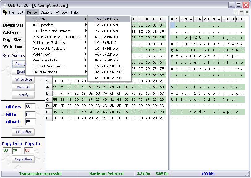
13 Memory Devices (EEPROM, RAM, FRAM) Upon starting any memory type device, you will see a screen similar to the one shown below. Note that RAM/FRAM will be similar to EEPROM but it will not have a Page Size or Write Time. I²C Address A drop-down menu is provided which allows the user to select a valid address for the selected device type. Write Page Size Selection The Page Write Size defines the number of bytes that may be written in a single erase/write programming cycle. Smaller devices generally use an 8 or 16-byte pages while larger devices use up to 128 bytes per page. Check the device datasheet to find the appropriate page write Win-I2CUSB Software User s Manual Page 13

14 size for the device you are programming. If you do not know the page size, use a small page size such as 8 bytes. A smaller page size will require a longer total programming time for a device. Erase/Write Cycle Time Programming software must allow a certain period of time to elapse after writing a block of data to an EEPROM. This time is device dependent but is normally between 5ms and 40ms. A STOP condition must be performed before the erase/write cycle commences. Most EEPROMs will not respond to their address until the erase/write cycle has been completed. Data Grid The data grid consists of rows and columns. Each cell within the grid contains a two digit hexadecimal number. Each cell corresponds to a physical byte location within the memory device. For example, in the diagram below, cell 0x21 is highlighted (row 2, column 1). This translates to address 33 (decimal) in the device. The program calculates the physical address for you and displays it at the left side of the screen in the box labeled Word Address or Subaddress. Byte Address (Subaddress) The byte address (sometimes called subaddress or word address) is a pointer to a register or memory location within the I²C device. To access this location, the software will send out the device I²C address, followed by this byte address, followed by the read or write data. The program displays the byte address of the active cell of the memory grid in both hexadecimal and decimal notation. Read Byte Button Pressing the 'Read Byte' button initiates a read from the I²C device. The program begins the transmission by writing the device address, followed by the current byte address. A Repeated Start is then generated, followed by the device s read address, and finally a read of a single data byte. The result of each byte read is immediately entered in the appropriate cell in the grid. Alternatively, you may press the <Alt> and <b> keys simultaneously to achieve the same results. Read All Button Pressing the 'Read All' button initiates a read from the I²C device. The program begins the transmission by writing the device address, then the byte address 0x00. A Repeated Start is then generated, followed by sequential reads of the entire device. In addition to pressing the 'Read All' button, you may press the <Alt> and <r> keys simultaneously to achieve the same results. Write Byte Button Pressing the 'Write Byte' button initiates a Write to the I²C device. The program begins the transmission by writing the slave address and then the word address of the currently active cell in the grid. The selected data byte is then sent. In addition to pressing the 'Write Byte' button, you may press the <Alt> and <y> keys simultaneously to achieve the same results. Write All Button Pressing the 'Write All' button initiates a Write to the I²C device. The program begins the transmission by Win-I2CUSB Software User s Manual Page 14
 followed by a STOP condition.")
15 writing the byte address 0x00 to the device and sequentially writes the entire device. For a RAM type device, the data is sent in one long message. In the case of an EEPROM, the software will send one page of data (usually 8 bytes but check the datasheet for the particular device you are addressing) followed by a STOP condition. Following the STOP condition, the program waits a length of time, determined by the Erase/Write cycle time of the device (again check the datasheet for the device you are programming), before writing another page to the device. In addition to pressing the 'Write All' button, you may press the <Alt> and <w> keys simultaneously to achieve the same results. After the completion of the write cycle, Win-I2CUSB will read the entire device to verify that the contents of the device match the data that was sent. An error message will be displayed if the data read from the device does not match the data in the on-screen buffer. Verify Button Pressing the Verify button initiates a read of the entire EEPROM. After reading the contents of the EEPROM, Win-I2CUSB will compare the contents with the values in the grid. An error will be flagged if the contents of the EEPROM do not match the contents of the Win-I2CUSB on-screen grid. Fill Buffer The grid will be filled with the two digit hexadecimal number found in the Fill with edit box when the Fill Buffer button is pressed. The fill can be constrained to the addresses found in the Fill from to the Fill to edit boxes. No information will be sent over the I²C bus. Checkerboard The grid will be filled an alternating 1 and 0 pattern when this is chosen from the Fill with Checkerboard selection is made on the Edit menu. Inverted Checkerboard The grid will be filled an alternating 0 and 1 pattern when this is chosen from the Fill with Inverted Checkerboard selection is made on the Edit menu. Win-I2CUSB Software User s Manual Page 15


16 Goto Byte... When the Go To Byte menu selection is made from the Edit menu, a dialog box is displayed where a hex or decimal address may be entered. When the OK button is pressed the grid location with the desired address is shown. This is useful when you don t want to scroll through to find a specific data location. Copy Block It is possible to copy a block of data from one on-screen buffer area to another using the Copy Block function. Simply define the data to be copied using the Copy From edit boxes and then enter the address where the data is to be copied to. The ending address is calculated automatically by the software and is not editable by the user. Pressing the Copy Block button starts the copying process. Win-I2CUSB Software User s Manual Page 16

17 Universal Interfaces User Definable Device The User Definable Device allows you to define your own I²C device and then enables the user to change the values of the individual cells within the grid using various controls such as sliders and spin controls. When the User Definable Device is first opened, a 256 byte device grid is shown on the screen but does not have any names associated with the data, and all the data bytes are set to 0xFF. A previously defined device may be loaded by selecting it from the Most Recently Used files at the bottom of the File menu. If devices have not yet been defined, there will be no devices shown below the File/Exit menu item. To begin the definition process, you may right click with your mouse on any data cell in the grid or select 'Current Device' or 'Current Cell' from the Edit menu. The Reset item in the Edit menu will clear all the register names to 'Undefined Register' and set the data values to 0xFF. Clicking on the desired cell and doing one of the following can change the data value of the individual cells: 1. Typing in a two digit hexadecimal number. 2. Assigning a slider to the active cell by pressing the Slider button. 3. Assigning a spin control to the active cell by pressing the Spinner button. 4. Assigning a Bit-wise control to the active cell by pressing the Bit-wise button. Items 2, 3, and 4 can also be achieved by positioning the cursor over the desired cell and right clicking on the grid to select the appropriate control from the pop-up menu. Define New Device This is similar to the Edit Current Device (explained below). This menu selection allows the user to start a new device from scratch. All register names are undefined and all default values are 0xFF. Win-I2CUSB Software User s Manual Page 17

18 Open Device Definition File A previously saved device definition file (.def) can be recalled by selecting this menu item. The device definition file contains the Device Name, Device Address, Register Names, and Register Values. Save Device definition files can be saved to disk by selecting the Save menu item. Save As Use the Save As dialog box to change the definition file name or to save the definition file in a new location. If the file name already exists, Win-I2CUSB asks if you want to replace the existing file. Save Registers in text format The device definition files are not in a format that can easily be used by the user, therefore, Win-I2CUSB allows you to save the information in a text format (extension.txt). Users can then open and edit this file with any word processor such as Notepad or WordPad. The text files are for the user s information only and cannot be read by Win-I2CUSB. Byte Mode When the Write All and Read All buttons are pressed, the software assumes that the subaddress is autoincremented after each data byte is written or read. For example, if you have a four byte device, the writing sequence would be Start-Address-Subaddress0-data0-data1-data2-data3-Stop. Many devices do not auto-increment the subaddress between data bytes and require that only one data byte is sent for each transmission. In these situations, click on the Byte Mode check box. The writing sequence would be Start- Address-Subaddress0-data0-Stop. The sequence would be repeated for each data byte. Print Device Data A print out of the register definitions can be obtained by selecting this option from the File menu. Data Grid The grid consists of rows and columns. Each cell within the grid contains a two digit hexadecimal number. Each cell corresponds to a physical byte location within the I²C device. For example, in the diagram shown above, cell 0x07 is highlighted (row 0, column 7). This translates to address 7 (decimal) in the device (assuming the first byte is address 0x00). The data may be changed by entering hexadecimal numbers from your keyboard. Non-valid keys will be ignored. In order to edit the entire grid, including the name and default values of the registers, you may right click on the grid or select the appropriate item from the Edit menu. The individual cells within the grid will be blue if the cell's subaddress is greater than the maximum number of registers defined for the active device. The number of device registers may be changed at any time in the Edit Current Device screen. Edit Menu The Edit menu is available only when the User Definable Device screen is active. The user can select from one of the three menu items: 1. Current Device - brings up a screen showing the all the register data for the active device. 2. Current register - allows registers to be changed one at a time. 3. Reset grid - all register data will be set to 0xFF and the register descriptions will be 'Undefined Register' Edit Current Register If you want to adjust one register in the grid, use the 'Edit Current Register' screen. This screen can be started by right clicking on the User Definable Device grid or by selecting Current Register from the Edit menu. The name of the register and the initial value displayed, when the definition file is first opened, can be changed here. Note that the register name changes are not saved until the Save or Save As.. item (under the File menu) is selected. Edit Current Device Editing the current device may be accomplished by clicking on 'Edit Current Device' from the Edit menu, Win-I2CUSB Software User s Manual Page 18


19 or by right clicking on the grid within the User Definable Device mode of Win-I2CUSB. The screen, shown above will be displayed when either method is invoked. Device Name: the name entered in this box will be shown in the title bar of Win-I2CUSB when the definition file is opened. Device Address: is the device I²C address that will be displayed in the Address box when the definition file is opened. Note that only even addresses are valid here. Win- I2CUSB will append the appropriate R/W bit at the end of the address depending upon the operation to be performed (the last bit will be a '1' if it is a read operation and a '0' if it is a write). Number of Registers: Enter the number of registers the device contains. The size of the data entry grid will be modified to accommodate the number of registers. Fill: This box should be modified only if you want to initialize all the registers to one particular value. OK button: the data entered by the user in the 'Edit Current Device' screen will be transferred to the User Definable Device screen. Cancel button: the editing session will be closed and no changes to the User Definable Device screen will occur. Note that any changes are not saved until the Save or Save As menu item is selected. Slider Control The Slider Control is activated when the user presses the Slider button on the User Defined Device screen or by right clicking the grid and then selecting 'Change Active Register with Slider Control' from the pop-up menu. The subaddress of the active cell in the grid will be assigned to the Slider. The subaddress is shown in the upper left corner. Moving the slider bar up and down will cause the value of that cell to be changed. If Auto Write On is checked, then the contents of the cell will be transmitted to the device subaddress when it is changed. If an error is encountered while transmitting using Auto Write, Win-I2CUSB will turn off Auto Write and it will be up to the user to fix the error condition and re-enable Auto Write. It should be noted that the Slider Control always stays on top of all other devices within Win-I2CUSB. Spin Control The Spin Control is activated when the user presses the Spinner button on the User Defined Device screen or by right clicking the grid and then selecting 'Increment/Decrement Current Register with a Spin Control' from the pop-up menu. Win-I2CUSB Software User s Manual Page 19


20 The subaddress of the active cell in the grid will be assigned to the Spin Control. The subaddress is shown in the upper left corner. Clicking on the spin control's up or down arrow will cause the value of that cell to be incremented or decremented. If Auto Write On is checked, then the contents of the cell will be transmitted to the device subaddress when it is changed.. If an error is encountered while transmitting using Auto Write, Win-I2CUSB will turn off Auto Write and it will be up to the user to fix the error condition and re-enable Auto Write. It should be noted that the Spin Control always stays on top of all other devices within Win-I2CUSB. Bit Control The Bit Control is activated when the user presses the Bit Control button on the User Defined Device screen or by right clicking the grid and then selecting 'Use Bit Control to Change Active Register' from the pop-up menu. The subaddress of the active register in the grid will be assigned to the Bit Control. The subaddress is shown in the upper left corner. Clicking on any of the eight edit boxes will cause the value of that bit to be inverted. If Auto Write On is checked, then the contents of the cell will be transmitted to the device subaddress when it is changed. It should be noted that the Bit Control always stays on top of all other devices within Win-I2CUSB. Win-I2CUSB Software User s Manual Page 20

21 Expert Mode The figure below shows the Expert Mode screen. Open New Page Pressing this button opens a new blank page. There will be 32 empty rows (messages). Selecting New from the File menu while the Expert Mode is active will perform the same function. Open Data File A previously saved data file can be recalled by pressing the Open Data File button or by selecting Open from the File menu while the Expert Mode is active. A dialog box will be displayed allowing the user to navigate to the appropriate directory. Save Data The current data will be saved when this button is pressed. The user specifies the name and location of the file in a dialog box that is displayed after the button is pressed. A dialog box will be displayed which allows the user to navigate to the appropriate directory. The user can also perform the same function by selecting Save from the File menu while the Expert Mode screen is active. Close Expert Mode The Expert Mode screen is closed but Win-I2CUSB will not be terminated. Add a Row Inserts a new (blank) row after the current row. You can also use the Ctrl+Ins keyboard shortcut to insert a new row. Delete a Row Deletes the current row (current message). You can also use the Ctrl+Del keyboard shortcut to delete the current row. Win-I2CUSB Software User s Manual Page 21
 will be copied.")
. You can also use the Ctrl+V keyboard shortcut to paste the clipboard into the current row.")
22 Clear the current row The current row (message) will be cleared. The row will not be deleted but will appear blank. You can also use the Shift+Del keyboard shortcut to clear the current row. Copy the Current Row The current row (message) will be copied. Use the Paste command to paste it to a different row. You can also use the Ctrl+C keyboard shortcut to copy the current row. Paste Data Previously copied data will be pasted into the current row (message). You can also use the Ctrl+V keyboard shortcut to paste the clipboard into the current row. Compress Data All blank rows will be eliminated from the display. Here is an example of a display before compress: And here is the same screen after the compress: Win-I2CUSB Software User s Manual Page 22


23 It is not required to perform a compress but it does speed up the message transfer process since the application does not need to evaluate blank rows to see if there is data to be sent. Send Message The current message will be sent when this button is pressed. The current message number is shown below the Send Message button. To change the active message to be sent, single-click on the row of the data to be sent. Send All All the valid messages on the screen will be sent in order of the row number. The action will be performed one time. A message is valid if there is a minimum of an address within the message. Since the program tests for a valid message on each line within the message grid before sending the message, it is recommended (not required) to compress the data (see Compress Data above) to speed up the transfer. Send Sequence A sequence of messages will be sent when the Send Sequence button is pressed. The sequence editor is invoked by double-clicking on the sequence display. The sequence length can be up to 64 messages in length. The sequencer is limited to using messages 1 through 99. The Sequence Editor is shown below. Message Editor The i2c message cannot be edited directly in the Expert mode screen. Instead, an Expert Mode Editor is brought up either by double-clicking on a message or when the user attempts to type directly into one of the rows (messages) in the Expert Mode screen. Message Number The message being edited is shown at the top of the message editor screen. Win-I2CUSB Software User s Manual Page 23
24 Delay after message A delay, measured in milliseconds, can be inserted after a message. Device Address The I2C slave address is entered in the address box in hexadecimal notation. The least significant bit of the address is not important (can be a 1 or 0 ) since the Expert Mode will ensure that this is appropriate for the read/write transaction when the message is actually transmitted. Read/Write Selection The user can select a Read or Write transaction from the drop-down selection box. If a Read is chosen, then the Number of Bytes to Read box will be shown and the data entry area will be hidden. If a Write is chosen, the Number of Bytes to Read will be hidden and the data entry area will be shown. Stop? Sending a Stop condition after a message is optional. Normally, it is advisable to send the Stop condition. If a Stop condition is not sent, the clock line will be held low until the next message is sent. If a Stop is not sent, the next message will begin with a Restart condition rather than a Start condition. Message Data The Message Data area contains the location where the user can enter up to 128 data bytes in hexadecimal format. Blank data bytes will be ignored. GPIO Control The GPIO pins on the Win-I2CUSB hardware can be controlled using the GPIO control buttons on the toolbar of the Expert Mode screen. The OUT pin can be set high or low by clicking on one of the buttons shown below. The state of the IN pin can be read from the hardware by pressing the Read button. Win-I2CUSB Software User s Manual Page 24

25 IO Expanders PCA9500/PCA bit I2C I/O port with interrupt and 2K EEPROM The PCA9500 and PCA9501 are 8-bit I/O expanders with an on-board 2-kbit EEPROM. The eight quasi bidirectional data pins can be independently used as inputs or outputs to monitor board level status or activate indicator devices such as LEDs. The data for each Input or Output is kept in the corresponding Input or Output register. The system master can read all registers. Changing I/O Expander Data with Checkboxes The ports, labeled P7 P0 can be set high or low by clicking on them with a mouse. A high logic level is indicated with a light green color while a low logic level is shown as a dark green color. If a port state is changed, the data byte box in the write area will be updated to reflect the changes. The new data can be sent to the PCA950x by pressing the Write Button. If the Auto Write On is enabled (light green), any change in the state of the Write checkboxes or Write Data Byte will immediately be sent to the PCA950x. Read I/O Button Upon pressing the Read Button, the program will update the hexadecimal data shown beside the Write I/O button as well as show the state of the individual I/Os. The I/O port is low if the port is shown in dark green and is high if it is light green. Set Data All the cells of the memory grid will be filled with the two digit hexadecimal number found in the Preset edit box when the Set Data button is pressed. No information will be sent over the I²C bus. Win-I2CUSB Software User s Manual Page 25
26 Word Address The Word Address (also called subaddress) is a pointer to a register or memory location within the I²C device. To access this location, the software will send out the device I²C address, followed by this subaddress, followed by the read or write data. The program displays the subaddress of the active cell of the memory grid in both hexadecimal and decimal notation. Read Byte Button Pressing the 'Read Byte' button initiates a read from the I²C device. The program begins the transmission by writing the word address, found in the Word Address or Subaddress box, to the device. The word address of the currently selected cell is shown in the Word Address box on the screen. A Repeated Start is then generated, followed by a read of the single byte. The result of each byte read is immediately entered in the appropriate cell in the grid. In addition to pressing the 'Read Byte' button, you may press the <Alt> and <b> keys simultaneously to achieve the same results. Read All Button Pressing the 'Read All' button initiates a read from the I²C device. The program begins the transmission by writing the word address 0 to the device. A Repeated Start is then generated, followed by sequential reads of the entire device. In addition to pressing the 'Read All' button, you may press the <Alt> and <r> keys simultaneously to achieve the same results. Write Byte Button Pressing the 'Write Byte' button initiates a Write to the I²C device. The program begins the transmission by writing the slave address and then the word address of the currently active cell in the grid. The selected data byte is then sent. In addition to pressing the 'Write Byte' button, you may press the <Alt> and <y> keys simultaneously and achieve the same results. Write All Button Pressing the 'Write All' button initiates a Write to the I²C device. The program begins the transmission by writing the word address 0 to the device and sequentially writes the entire device. The software will send one page of data (4 bytes) followed by a STOP condition. Following the STOP condition before writing another page to the device. In addition to pressing the 'Write All' button, you may press the <Alt> and <w> keys simultaneously to achieve the same results. After the completion of the write cycle, Win-I2CUSB will read the entire device to verify that the contents of the device match the data that was sent. An error message will be displayed if the data is not verified. Win-I2CUSB Software User s Manual Page 26
 expansion for I2C/SMBus applications The PCA9554 and PCA9554A are similar devices but respond to different i2c addresses.")
27 PCA9534/PCA9538/PCA9554/PCA9554A 8-bit I/O Expanders with Interrupt The PCA9534, PCA9538, PCA9554, and PCA9554A are 16-pin CMOS devices that provide 8 bits of General Purpose parallel Input/Output (GPIO) expansion for I2C/SMBus applications The PCA9554 and PCA9554A are similar devices but respond to different i2c addresses. The PCA9534 differs from the PCA9554(A) in that it does not have pull-up resistors on the outputs. These devices have four registers. All four registers can be read by the bus master while the Input register can only be read. Automatic Write Enable When Auto Write is enabled (light green), any changes made to Registers 1, 2, or 3 checkboxes will cause the program to write the new data to the device. The display will read 'Auto Write Off' in when it is disabled and 'Auto Write On' in when enabled. Checkboxes The checkboxes indicate the logic level of the various bits in the registers. A checked box is equivalent to logic 1 while an unchecked box is equivalent to a logic 0. The logic level can be changed by single clicking on the checkbox. If Auto Write is enabled (checked), Win-I2CUSB will write the new value to the device shown in the Address box. The checkboxes will also be updated when a new value is read by Win- I2CUSB, or when the value in the edit boxes are changed. Edit Boxes The edit boxes show the current hexadecimal value for each of the 4 registers. Register 0 is a Read-Only register so the user cannot change this value. If the hexadecimal value is changed by the user, it will be transmitted by Win-I2CUSB if the Auto Write is enabled (checked). The checkboxes will also be updated to reflect any changes to the values of the Edit Box. Read Buttons Upon pressing one of the Read Buttons, Win-I2CUSB will read the appropriate register and place the Win-I2CUSB Software User s Manual Page 27
28 hexadecimal value in the edit box. The checkboxes are updated to reflect the individual bit logic levels. Pressing the Read All button reads all four registers. Because these devices do not automatically increment the register address between operations, only one register may be read in each transaction. Therefore, after Register 0 has been read, Win-I2CUSB will begin a new transaction for each of the other registers. This will continue until all four registers have been read. Write Button Upon pressing one of the Write Buttons, Win-I2CUSB will write to the appropriate register. Pressing the Write All button writes to Registers 1, 2, and 3. Since there is no automatic increment of the register subaddress between writes, only one register may be written for each Start condition. Therefore, after Register 1 has been written by Win-I2CUSB, a new transaction will be sent out so that Register 2 can be written, followed by Register 3. Win-I2CUSB Software User s Manual Page 28

29 PCA9535/PCA9555/PCA bit I/O Expanders with interrupt The PCA9555 and PCA9535 are 24-pin CMOS device that provide 16 bits of General Purpose parallel Input/Output (GPIO) expansion for I 2 C/SMBus applications and were developed to enhance the NXP family of I 2 C I/O expanders. The improvements include higher drive capability, 5V I/O tolerance, lower supply current, individual I/O configuration, and smaller packaging. I/O expanders provide a simple solution when additional I/O is needed for ACPI power switches, sensors, pushbuttons, LEDs, fans, etc. The PCA9555 consist of two 8-bit Configuration (Input or Output selection); Input, Output and Polarity inversion (Active high or Active low operation) registers. The system master can enable the I/Os as either inputs or outputs by writing to the I/O configuration bits. The data for each Input or Output is kept in the corresponding Input or Output register. The polarity of the read register can be inverted with the Polarity Inversion Register. All registers can be read by the system master. The PCA9539 is identical to the PCA9555 except for the removal of the internal I/O pull-up resistor which greatly reduces power consumption when the I/Os are held LOW, repleacement of A2 with RESET and different address range. Input Registers (subaddress 0x00 and 0x01) These registers are read-only. They reflect the incoming logic levels of the pins, regardless of whether the pin is defined as an input or an output by the Configuration Registers. Writes to this register have no effect. Output Registers (subaddress 0x02 and 0x03) These registers reflect the outgoing logic levels of the pins defined as outputs by the Configuration Registers. Bit values in this register have no effect on pins defined as inputs. Reads from this register return the value that is in the flip-flop controlling the output selection, NOT the actual pin value. Polarity Registers (subaddress 0x04 and 0x05) These registers allow the user to invert the polarity of the Input Port Register data. If a bit in this register is set (written with 1 ), the corresponding Input Port data is inverted. If a bit in this register is cleared (written with a 0 ), the Input Port data polarity is retained. Win-I2CUSB Software User s Manual Page 29
30 Configuration Register (subaddress 0x06 and 0x07) The Configuration Registers define the directions of the I/O pins. If a bit in these register is set, the corresponding port pin is enabled as an input with high impedance output driver. If a bit in these registers is cleared, the corresponding port pin is enabled as an output. At reset, the I/Os are configured as inputs with a weak pull-up to VDD. Automatic Write Enable When Auto Write On is enabled (green), any changes made to Registers 1 through 7 checkboxes will cause the program to write the new data to the PCA9555. The display will read 'Auto Write Off' when it is disabled and 'Auto Write On' when enabled. Checkboxes The checkboxes indicate the logic level of the various bits in the registers. A checked box is equivalent to logic 1 while an unchecked box is equivalent to a logic 0. The logic level can be changed by single clicking on the checkbox. If Auto Write is enabled (green LED), Win-I2CUSB will write the new value to the PCA9555 immediately after a change is made. Edit Boxes The edit boxes show the current hexadecimal value for each of the 4 registers. Register 0 is a Read-Only register so the user cannot change this value. If the hexadecimal value is changed by the user, it will be transmitted by Win-I2CUSB if the Auto Write is on (checked). The checkboxes will also be updated to reflect the new value of the Edit Box. Read Buttons Upon pressing one of the Read Buttons, Win-I2CUSB will read the appropriate register and place the hexadecimal value in the edit box. The checkboxes are updated to reflect the individual bit logic levels. In the top left corner of the button, there is a plus (+) sign. Clicking on the (+) brings up a menu above button. The menu allows the user to change the function of the button so that either the low or high register can be read or both can be read. Win-I2CUSB Software User s Manual Page 30

31 PCA9556/PCA bit I/O Expander with Reset The PCA9556 and PCA9557 are CMOS circuit that provides parallel input/output expansion for I 2 C and SMBus applications. These devices consist of an 8-bit input port register, 8-bit output port register, and a I 2 C interface. It has low current consumption and a high impedance open drain output pin, I/O0. The system master can reset the PCA9556 in the event of a timeout by asserting a LOW on the reset input. The system master can also invert the PCA9556/PCA9557 inputs by writing to their active HIGH polarity inversion bits. Finally, the system master can enable the I/Os as either inputs or outputs by writing to the I/O configuration register. Auto Write When the Auto Write On is enabled (green), any changes made by the user to the PCA9556/PCA9557 Registers 1, 2, and 3 will immediately be sent to the PCA9556/PCA9557. If an error is encountered during this transmission, Auto Write Off will be displayed (red). Read All Button Each time the Read All button is pressed, the contents of Registers 0, 1, 2, and 3 are read from the PCA9556/PCA9557. The register data will be reflected in the state of the checkboxes, with an unchecked box indicating logic '0' and a checked box indicating logic '1'. Write All Button When this button is pressed, Registers 1, 2, and 3 are written to the PCA9556/PCA9557. Register 0 is a read-only register. Register 0 (Input Port) This register is an input-only port. It reflects the incoming logic levels of the pins, regardless of whether the pin is defined as an input or an output by register 3. Writes to this register have no effect. Logic '0' is shown as an unchecked checkbox while logic '1' is shown as a checked box. Register 1 (Output port) This register is an output-only port. It reflects the outgoing logic levels of the pins defined as outputs by Win-I2CUSB Software User s Manual Page 31
32 register 3. Bit values in this register have no effect on pins defined as inputs. In turn, reads from this register reflect the value that is in the flip-flop controlling the output selection, NOT the actual pin value. Register 2 (Polarity) This register enables polarity inversion of pins defined as inputs by register 3. If a bit in this register is set (written with 1 ), the corresponding port pin s polarity is inverted. If a bit in this register is cleared (written with a 0 ), the corresponding port pin s original polarity is retained. Register 3 (Configuration) This register is an input-only port. It reflects the incoming logic levels of the pins, regardless of whether the pin is defined as an input or an output by register 3. Writes to this register have no effect. This register configures the directions of the I/O pins. If a bit in this register is set (written with 1 ), the corresponding port pin is enabled as an input with high impedance output driver. If a bit in this register is cleared (written with 0 ), the corresponding port pin is enabled as an output. Win-I2CUSB Software User s Manual Page 32
. The system master can enable the I/Os as either inputs or outputs by writing to the I/O configuration bits.")
33 PCA9536/PCA bit I/O Expanders with Reset The PCA9536 and PCA9537 consist of a 4-bit Configuration register (input or output selection), 4-bit Input Port register, 4-bit Output Port register and a 4-bit Polarity Inversion register (active HIGH or active LOW operation). The system master can enable the I/Os as either inputs or outputs by writing to the I/O configuration bits. The data for each input or output is kept in the corresponding Input Port or Output Port register. The polarity of the read register can be inverted with the Polarity Inversion register. All registers can be read by the system master. Auto Write When the Auto Write On is enabled (green), any changes made by the user to the PCA9536/PCA9537 Registers 1, 2, and 3 will immediately be sent to the PCA9536/PCA9537. If an error is encountered during this transmission, Auto Write Off will be displayed (red). Read All Button Each time the Read All button is pressed, the contents of Registers 0, 1, 2, and 3 are read from the PCA9536/PCA9537. The register data will be reflected in the state of the checkboxes, with an unchecked box indicating logic '0' and a checked box indicating logic '1'. Write All Button When this button is pressed, Registers 1, 2, and 3 are written to the PCA9536/PCA9537. Register 0 is a read-only register. Register 0 (Input Port) This register is an input-only port. It reflects the incoming logic levels of the pins, regardless of whether the pin is defined as an input or an output by register 3. Writes to this register have no effect. Logic '0' is shown as an unchecked checkbox while logic '1' is shown as a checked box. Register 1 (Output port) This register is an output-only port. It reflects the outgoing logic levels of the pins defined as outputs by register 3. Bit values in this register have no effect on pins defined as inputs. In turn, reads from this register reflect the value that is in the flip-flop controlling the output selection, NOT the actual pin value. Win-I2CUSB Software User s Manual Page 33
34 Register 2 (Polarity) This register enables polarity inversion of pins defined as inputs by register 3. If a bit in this register is set (written with 1 ), the corresponding port pin s polarity is inverted. If a bit in this register is cleared (written with a 0 ), the corresponding port pin s original polarity is retained. Register 3 (Configuration) This register is an input-only port. It reflects the incoming logic levels of the pins, regardless of whether the pin is defined as an input or an output by register 3. Writes to this register have no effect. This register configures the directions of the I/O pins. If a bit in this register is set (written with 1 ), the corresponding port pin is enabled as an input with high impedance output driver. If a bit in this register is cleared (written with 0 ), the corresponding port pin is enabled as an output. Win-I2CUSB Software User s Manual Page 34

35 PCF8574/PCF8574A 8-bit I/O Expander The PCF8574 provides general-purpose remote I/O expansion for most microcontroller families via the I²C bus. The device consists of an 8-bit quasi bi-directional port and an I²C interface. The PCF8574 has low current consumption and includes latched outputs with high current drive capability for directly driving LEDs. It also possesses an open-drain interrupt output that can be connected to the interrupt logic of the microcontroller. By sending an interrupt signal on this line, the remote I/O can inform the microcontroller if there is incoming data on its ports without having to communicate via the I²C bus. This means that the PCF8574 can remain a simple slave device. The PCF8574 and PCF8574A differ only in their slave addresses (as shown below). Checkboxes The checkboxes, labeled P0 - P7, in the write areas of the PCF8574(A) screen can be checked/unchecked by clicking on them with a mouse. If a checkbox state is changed, the data byte box in the write area will be updated to reflect the changes. The new data can be sent to the PCF8574(A) by pressing the Write Button. If the Auto Write On is checked, any change in the state of the Write checkboxes or Write Data Byte will immediately be sent to the PCF8574(A). The checkboxes found in the Read PCF8574(A) panels are read only and can only be changed by the software by clicking the Read buttons. If a checkbox is checked, this indicates a logic '1', while an unchecked box indicates a logic '0'. Read Button Upon pressing the Read Button, the program will update the hexadecimal data shown beside the button as well as show the state of the individual I/Os. The I/O is low if the checkbox is unchecked and high if it is checked. Read Data The Read boxes on the PCF8574(A) screens are read-only. The user cannot change the contents of any edit boxes or checkboxes in this area. The information is updated only by pressing the Read Button. Data read from the PCF8574(A) will be shown in the box beside the Read Button. The checkboxes are then changed to show the value of each individual I/O of the device. If the checkbox is checked, then the Win-I2CUSB Software User s Manual Page 35
36 I/O pin is high while an unchecked box means that the I/O pin is low. It is important to remember that before any I/Os in the PCF8574(A) can be used as inputs, they must be set high first. The program does not do this for you. Data Byte Any two digit hexadecimal number may be entered in this data box. When it is changed, the checkboxes labeled P0 - P7 will also change showing the current value of the data which will be written to the PCF8574(A). Write Button Pressing the Write Button will send an I²C message to the PCF8574(A) consisting of: a Start condition, the I²C address, the data byte, followed by the Stop condition. Note that if Automatic Write Enable is checked, any changes to the data box will be sent any time a change is made. Automatic Write Enable When Auto Write On is enabled (light green), any changes made to the P0-P7 checkboxes will cause the program to write the new data to the PCF8574(A). The display will read 'Auto Write Off' when it is disabled and 'Auto Write On' when enabled. Auto Readback When this function is enabled (light green), the software will immediately read the PCF8574 after it has performed a write. The result of the read will be displayed in the Read groupbox. Win-I2CUSB Software User s Manual Page 36

37 PCF bit I/O Expander The PCF8575 is a CMOS circuit which provides general purpose remote I/O expansion for most microcontroller families via the two-line bi-directional bus (I²C-bus). The device consists of a 16-bit quasi bi-directional port and an I²C-bus interface. The PCF8575 has a low current consumption and includes latched outputs with high current drive capability for directly driving LEDs. It also possesses an interrupt line (INT) which can be connected to the interrupt logic of a microcontroller. By sending an interrupt signal on this line, the remote I/O can inform the microcontroller if there is incoming data on its ports without having to communicate via the I²C bus. This means that the PCF8575 is an I²C-bus slave transmitter/receiver. Every data transmission from the PCF8575 must consist of an even number of bytes, the first byte will be referred to as P07 to P00 and the second byte as P17 to P10. The third will be referred to as P07 to P00 and so on. Read Checkboxes There are sixteen checkboxes in the Read box. The contents of the PCF8575 are read by pressing the Read button. A checked item indicates logic '1' while an unchecked item means logic '0'. The user cannot change the checkboxes since these are read-only. Write Checkboxes Clicking on the checkboxes will invert the current state of the bit. A logic '0' is shown as an unchecked box while a logic '1' is shown as a checked box. If Auto Write is on, then any changes made to these checkboxes will immediately be sent to the PCF8575. Read Button When this button is pressed, the two eight bit registers are read via the I²C bus. Data from Port 0 is read first, followed by Port 1. The data bytes are displayed in the area beside the Read button and the checkboxes are updated. Write Button When the Write button is pressed, the contents of the High and Low data boxes are sent to the PCF8575 via the I²C bus. Win-I2CUSB Software User s Manual Page 37
38 Read Data Boxes These two boxes show the port state of the PCF8575 in hexadecimal format. These boxes cannot be directly modified by the user but must be changed by pressing the read button. Write Data Boxes The user can change the contents of the register by entering a two digit hexadecimal number into the upper and/or lower edit boxes. If the Auto Write is enabled, both data registers are sent, even if only one is changed. Auto Write When the Auto Write is enabled (light green), any changes made by the user to the PCF8575 checkboxes on the screen will immediately be sent to the PCF8575 via the I²C bus. Win-I2CUSB Software User s Manual Page 38
 timer. The uniqueness of this device is the internal oscillator with two programmable blink rates.")
39 LED Blinkers and Dimmers PCA bit I2C LED Dimmer The PCA955x LED Blinker blinks LEDs in I 2 C applications where it is necessary to limit bus traffic or free up the I 2 C Master s (MCU, MPU, DSP, chipset, etc.) timer. The uniqueness of this device is the internal oscillator with two programmable blink rates. To blink LEDs using normal I/O Expanders like the PCF8574 or PCA9554, the bus master must send repeated commands to turn the LED on and off. This greatly increases the amount of traffic on the I 2 C bus and uses up one of the master s timers. The PCA955x LED Blinker instead requires only the initial set up command to program BLINK RATE 1 and BLINK RATE 2 (i.e., the frequency and duty cycle) for each individual output. Device Address The device I2C address can be selected by choosing one of the hexadecimal selections from the drop down list. The default address at start-up is 0xC0. Auto Write On/Off Button When Auto Write is disabled (LED off), the software can be modifed without transmitting data to through the parallel port. When the Auto Write LED is On, any changes made to the software is immediately transmitted to the PCA955x. LED Mode Selector Each LED can be set in one of four modes: ON, OFF, PWM0, and PWM1. The mode is selected by moving the switches to the appropriate mode for the LED. All LEDs set to PWMx will blink at the same frequency, duty cycle, and phase. PWM Period Slidebar The period of the PCA955x can be changed by moving the PWM0 or PWM1 slidebars. The period (in seconds) and frequency (in Hertz) is displayed below the slidebar. The actual value of the PCA955x register is displayed in the Registers groupbox. Win-I2CUSB Software User s Manual Page 39
40 PWM Duty Cycle The duty cycle for PWM0 and PWM1 can be changed by moving the PWM0 or PWM1 slidebars. The duty cycle is displayed (in percent) below the slidebar. The actual value of the PCA955x register is dispalyed in the Registers groupbox. Write All Button Pressing the Write All button causes Registers 1 through 6 to be programmed. Read Input Register When the Read Input register button is pressed, the Input register is read and the data is presented in the Registers groupbox. Read All Button Pressing the Read All button will read all the device registers from the PCA955x using the auto-increment feature. Since the PCA955x devices don t allow auto-increment starting from Register 0, the reads start with the register with the highest address which causes the auto-increment pointer to roll-over to Register 0 (Input Register). The reads continue until the all the registers have been read. The data will be displayed in the Registers groupbox and the controls (sliders, switches) will be updated. Win-I2CUSB Software User s Manual Page 40
, the software can be modifed without transmitting data to through the parallel port.")
41 PCA bit I2C LED Dimmer Device Address The device I2C address can be selected by choosing one of the hexadecimal selections from the drop down list. The default address at start-up is 0xC0. Auto Write On/Off Button When Auto Write is disabled (LED off), the software can be modifed without transmitting data to through the parallel port. When the Auto Write LED is On, any changes made to the software is immediately transmitted to the PCA9531. LED Mode Selector Each LED can be set in one of four modes: ON, OFF, PWM0, and PWM1. The mode is selected by moving the switches to the appropriate mode for the LED. All LEDs set to PWMx will blink at the same frequency, duty cycle, and phase. PWM Period Slidebar The period of the PCA9531 can be changed by moving the PWM0 or PWM1 slidebars. The period (in seconds) and frequency (in Hertz) is displayed below the slidebar. The actual value of the PCA9531 register is displayed in the Registers groupbox. PWM Duty Cycle The duty cycle for PWM0 and PWM1 can be changed by moving the PWM0 or PWM1 slidebars. The duty cycle is displayed (in percent) below the slidebar. The actual value of the PCA9531 register is dispalyed in the Registers groupbox. Write All Button Pressing the Write All button causes Registers 1 through 6 to be programmed. Win-I2CUSB Software User s Manual Page 41
42 Read Input Register When the Read Input register button is pressed, the Input register is read and the data is presented in the Registers groupbox. Read All Button Pressing the Read All button will read all the device registers from the PCA9531 using the auto-increment feature. Since the PCA955x devices don t allow auto-increment starting from Register 0, the reads start with the register with the highest address which causes the auto-increment pointer to roll-over to Register 0 (Input Register). The reads continue until the all the registers have been read. The data will be displayed in the Registers groupbox and the controls (sliders, switches) will be updated. Win-I2CUSB Software User s Manual Page 42
, the software can be modifed without transmitting data to through the parallel port.")
43 PCA bit I2C LED Dimmer Device Address The device I2C address can be selected by choosing one of the hexadecimal selections from the drop down list. The default address at start-up is 0xC0. Auto Write On/Off Button When Auto Write is disabled (LED off), the software can be modifed without transmitting data to through the parallel port. When the Auto Write LED is On, any changes made to the software is immediately transmitted to the PCA9532. LED Mode Selector Each LED can be set in one of four modes: ON, OFF, PWM0, and PWM1. The mode is selected by moving the switches to the appropriate mode for the LED. All LEDs set to PWMx will blink at the same frequency, duty cycle, and phase. PWM Period Slidebar The period of the PCA9532 can be changed by moving the PWM0 or PWM1 slidebars. The period (in seconds) and frequency (in Hertz) is displayed below the slidebar. The actual value of the PCA9532 register is displayed in the Registers groupbox. PWM Duty Cycle The duty cycle for PWM0 and PWM1 can be changed by moving the PWM0 or PWM1 slidebars. The duty cycle is displayed (in percent) below the slidebar. The actual value of the PCA9532 register is dispalyed in the Registers groupbox. Write All Button Pressing the Write All button causes Registers 1 through 6 to be programmed. Win-I2CUSB Software User s Manual Page 43
44 Read Input Register When the Read Input register button is pressed, the Input register is read and the data is presented in the Registers groupbox. Read All Button Pressing the Read All button will read all the device registers from the PCA9532 using the auto-increment feature. Since these devices don t allow auto-increment starting from Register 0, the reads start with the register with the highest address which causes the auto-increment pointer to roll-over to Register 0 (Input Register). The reads continue until the all the registers have been read. The data will be displayed in the Registers groupbox and the controls (sliders, switches) will be updated. Win-I2CUSB Software User s Manual Page 44
, the software can be modifed without transmitting data to through the parallel port.")
45 PCA bit I2C LED Dimmer Device Address The device I2C address can be selected by choosing one of the hexadecimal selections from the drop down list. The default address at start-up is 0xC0. Auto Write On/Off Button When Auto Write is disabled (LED off), the software can be modifed without transmitting data to through the parallel port. When the Auto Write LED is On, any changes made to the software is immediately transmitted to the PCA9533. LED Mode Selector Each LED can be set in one of four modes: ON, OFF, PWM0, and PWM1. The mode is selected by moving the switches to the appropriate mode for the LED. All LEDs set to PWMx will blink at the same frequency, duty cycle, and phase. PWM Period Slidebar The period of the PCA9533 can be changed by moving the PWM0 or PWM1 slidebars. The period (in seconds) and frequency (in Hertz) is displayed below the slidebar. The actual value of the PCA9533 register is displayed in the Registers groupbox. PWM Duty Cycle The duty cycle for PWM0 and PWM1 can be changed by moving the PWM0 or PWM1 slidebars. The duty cycle is displayed (in percent) below the slidebar. The actual value of the PCA9533 register is dispalyed in the Registers groupbox. Write All Button Pressing the Write All button causes Registers 1 through 6 to be programmed. Win-I2CUSB Software User s Manual Page 45
46 Read Input Register When the Read Input register button is pressed, the Input register is read and the data is presented in the Registers groupbox. Read All Button Pressing the Read All button will read all the device registers from the PCA9533 using the auto-increment feature. Since the PCA955x devices don t allow auto-increment starting from Register 0, the reads start with the register with the highest address which causes the auto-increment pointer to roll-over to Register 0 (Input Register). The reads continue until the all the registers have been read. The data will be displayed in the Registers groupbox and the controls (sliders, switches) will be updated. Win-I2CUSB Software User s Manual Page 46
, the software can be modifed without transmitting data to through the parallel port.")
47 PCA bit I2C LED Blinker Device Address The device I2C address can be selected by choosing one of the hexadecimal selections from the drop down list. The default address at start-up is 0xC0. Auto Write On/Off Button When Auto Write is disabled (LED off), the software can be modifed without transmitting data to through the parallel port. When the Auto Write LED is On, any changes made to the software is immediately transmitted to the PCA9550. LED Mode Selector Each LED can be set in one of four modes: ON, OFF, PWM0, and PWM1. The mode is selected by moving the switches to the appropriate mode for the LED. All LEDs set to PWMx will blink at the same frequency, duty cycle, and phase. PWM Period Slidebar The period of the PCA9550 can be changed by moving the PWM0 or PWM1 slidebars. The period (in seconds) and frequency (in Hertz) is displayed below the slidebar. The actual value of the PCA9550 register is displayed in the Registers groupbox. PWM Duty Cycle The duty cycle for PWM0 and PWM1 can be changed by moving the PWM0 or PWM1 slidebars. The duty cycle is displayed (in percent) below the slidebar. The actual value of the PCA9550 register is dispalyed in the Registers groupbox. Write All Button Pressing the Write All button causes Registers 1 through 5 to be programmed. Win-I2CUSB Software User s Manual Page 47
48 Read Input Register When the Read Input register button is pressed, the Input register is read and the data is presented in the Registers groupbox. Read All Button Pressing the Read All button will read all the device registers from the PCA9550 using the auto-increment feature. Since the PCA955x devices don t allow auto-increment starting from Register 0, the reads start with the register with the highest address which causes the auto-increment pointer to roll-over to Register 0 (Input Register). The reads continue until the all the registers have been read. The data will be displayed in the Registers groupbox and the controls (sliders, switches) will be updated. Win-I2CUSB Software User s Manual Page 48
, the software can be modifed without transmitting data to through the parallel port.")
49 PCA bit I2C LED Blinker Device Address The device I2C address can be selected by choosing one of the hexadecimal selections from the drop down list. The default address at start-up is 0xC0. Auto Write On/Off Button When Auto Write is disabled (LED off), the software can be modifed without transmitting data to through the parallel port. When the Auto Write LED is On, any changes made to the software is immediately transmitted to the PCA9551. LED Mode Selector Each LED can be set in one of four modes: ON, OFF, PWM0, and PWM1. The mode is selected by moving the switches to the appropriate mode for the LED. All LEDs set to PWMx will blink at the same frequency, duty cycle, and phase. PWM Period Slidebar The period of the PCA9551 can be changed by moving the PWM0 or PWM1 slidebars. The period (in seconds) and frequency (in Hertz) is displayed below the slidebar. The actual value of the PCA9551 register is displayed in the Registers groupbox. PWM Duty Cycle The duty cycle for PWM0 and PWM1 can be changed by moving the PWM0 or PWM1 slidebars. The duty cycle is displayed (in percent) below the slidebar. The actual value of the PCA9551 register is dispalyed in the Registers groupbox. Write All Button Pressing the Write All button causes Registers 1 through 6 to be programmed. Win-I2CUSB Software User s Manual Page 49
50 Read Input Register When the Read Input register button is pressed, the Input register is read and the data is presented in the Registers groupbox. Read All Button Pressing the Read All button will read all the device registers from the PCA9551 using the auto-increment feature. Since the PCA955x devices don t allow auto-increment starting from Register 0, the reads start with the register with the highest address which causes the auto-increment pointer to roll-over to Register 0 (Input Register). The reads continue until the all the registers have been read. The data will be displayed in the Registers groupbox and the controls (sliders, switches) will be updated. Win-I2CUSB Software User s Manual Page 50
, the software can be modifed without transmitting data to through the parallel port.")
51 PCA bit I2C LED Blinker Device Address The device I2C address can be selected by choosing one of the hexadecimal selections from the drop down list. The default address at start-up is 0xC0. Auto Write On/Off Button When Auto Write is disabled (LED off), the software can be modifed without transmitting data to through the parallel port. When the Auto Write LED is On, any changes made to the software is immediately transmitted to the PCA9552. LED Mode Selector Each LED can be set in one of four modes: ON, OFF, PWM0, and PWM1. The mode is selected by moving the switches to the appropriate mode for the LED. All LEDs set to PWMx will blink at the same frequency, duty cycle, and phase. PWM Period Slidebar The period of the PCA9552 can be changed by moving the PWM0 or PWM1 slidebars. The period (in seconds) and frequency (in Hertz) is displayed below the slidebar. The actual value of the PCA9552 register is displayed in the Registers groupbox. PWM Duty Cycle The duty cycle for PWM0 and PWM1 can be changed by moving the PWM0 or PWM1 slidebars. The duty cycle is displayed (in percent) below the slidebar. The actual value of the PCA9552 register is dispalyed in the Registers groupbox. Write All Button Pressing the Write All button causes Registers 1 through 6 to be programmed. Read Input Register When the Read Input register button is pressed, the Input register is read and the data is presented in the Registers groupbox. Win-I2CUSB Software User s Manual Page 51
52 Read All Button Pressing the Read All button will read all the device registers from the PCA9552 using the auto-increment feature. Since the PCA955x devices don t allow auto-increment starting from Register 0, the reads start with the register with the highest address which causes the auto-increment pointer to roll-over to Register 0 (Input Register). The reads continue until the all the registers have been read. The data will be displayed in the Registers groupbox and the controls (sliders, switches) will be updated. Win-I2CUSB Software User s Manual Page 52
 timer. The uniqueness of this device is the internal oscillator with two programmable blink rates.")
53 PCA bit I2C LED Blinker The PCA9553 LED blinker blinks LEDs in I2C-bus and SMBus applications where it is necessary to limit bus traffic or free up the I2C-bus master's (MCU, MPU, DSP, chip set, etc.) timer. The uniqueness of this device is the internal oscillator with two programmable blink rates. Device Address The device I2C address can be selected by choosing one of the hexadecimal selections from the drop down list. The default address at start-up is 0xC0. Auto Write On/Off Button When Auto Write is disabled (LED off), the software can be modifed without transmitting data to through the parallel port. When the Auto Write LED is On, any changes made to the software is immediately transmitted to the PCA9553. LED Mode Selector Each LED can be set in one of four modes: ON, OFF, PWM0, and PWM1. The mode is selected by moving the switches to the appropriate mode for the LED. All LEDs set to PWMx will blink at the same frequency, duty cycle, and phase. PWM Period Slidebar The period of the PCA9553 can be changed by moving the PWM0 or PWM1 slidebars. The period (in seconds) and frequency (in Hertz) is displayed below the slidebar. The actual value of the PCA9553 register is displayed in the Registers groupbox. Win-I2CUSB Software User s Manual Page 53
54 PWM Duty Cycle The duty cycle for PWM0 and PWM1 can be changed by moving the PWM0 or PWM1 slidebars. The duty cycle is displayed (in percent) below the slidebar. The actual value of the PCA9553 register is dispalyed in the Registers groupbox. Write All Button Pressing the Write All button causes Registers 1 through 5 to be programmed. Read Input Register When the Read Input register button is pressed, the Input register is read and the data is presented in the Registers groupbox. Read All Button Pressing the Read All button will read all the device registers from the PCA9553 using the auto-increment feature. Since the PCA955x devices don t allow auto-increment starting from Register 0, the reads start with the register with the highest address which causes the auto-increment pointer to roll-over to Register 0 (Input Register). The reads continue until the all the registers have been read. The data will be displayed in the Registers groupbox and the controls (sliders, switches) will be updated. Win-I2CUSB Software User s Manual Page 54

55 SAA Digit LED-driver The circuit is especially designed to drive four 7-segment LED displays with decimal point by means of multiplexing between two pairs of digits. It features an I2C-Bus slave transceiver interface with the possibility to program four different SLAVE ADDRESSES, a POWER RESET flag, 16 current sink OUTPUTS, controllable by software up to 21 ma, two multiplex drive outputs for common anode segments, an on-chip multiplex oscillator, control bits to select static, dynamic and blank mode, and one bit for segment test. Control Register The Control Register is responsible for determining the mode of operation of the SAA1064. It can control which digits are blanked, static versus dynamic operation, and the current supplied to the LEDs. In order to change the value of the Control Register in the SAA1064, the state of the checkboxes in the Control Register box on the screen can be toggled (checked/unchecked) and the slider can be used to change the current sinking of the device. The figure below shows the contents of the Control Register. C6 = 1 adds 12mA to segment output current C5 = 1 adds 6mA to segment output current C4 = 1 adds 3mA to segment output current C3 = 1 all segment outputs are switched on for segment test C2 = 0/1 digits 2 and 4 are blanked/not blanked C1 = 0/1 digits 1 and 3 are blanked/not blanked C0 = 0 static mode (continuous display of digits 1 and 2) C0 = 1 dynamic mode (alternating display of digit and 2 + 4) Automatic Write If the Automatic Write is enabled (green), any changes to the SAA1064 Control Register or Digits will immediately be sent via the I²C bus. Win-I2CUSB Software User s Manual Page 55
56 The data sent to the SAA1064 consists of a Start condition, the I²C address, Instruction byte, then the data for the changed Control Register or Data byte, followed by the Stop condition. Therefore, a total of three bytes will be sent any time a change is made and Automatic Write is enabled. Digits 1, 2, 3, and 4 The SAA1064 can drive up to four 8-segment LEDs. The data for these digits is contained in four registers within the SAA1064. In order to change the contents of these registers, you can click on the LEDs within the Digit groupboxes. If an LED is on (light green), then the LED segment is on while a dark green LED causes the LED segment to turn off. Changes in the on-screen LEDs are reflected in the hexadecimal values shown above the on-screen LEDs. If the Automatic Write is enabled (light green), any changes to the SAA1064 Control Register or LED Digits will immediately be sent to the device through I²C bus. Instruction Byte The instruction byte is equivalent to a subaddress. The instruction byte is configured as shown below: The bits SC, SB and SA of the instruction byte form a pointer and determine to which register the data byte following the instruction byte will be written. All other bytes will then be stored in the registers with consecutive subaddresses. This feature is called Auto-Increment (AI) of the subaddress and enables a quick initialization by the master. The subaddress pointer will wrap around from 7 to 0. The Win-I2CUSB software does not allow the user to modify the instruction byte. The software points to 00h when the write button is pressed since it will be writing all the registers. When Automatic Write is enabled, the instruction byte will point to the register that is affected by the changes. For example, if the user clicks on Bit 5 in Digit 4, then the software will set the instruction byte to 04h for the write sequence. Read Address This box reflects the I²C address that is sent to the SAA1064 when a read operation is performed. The contents of this box cannot be changed directly by the user, but can only be changed by clicking on a different address in the Device Address box. Status Register Only one bit is present in the status byte: the Power Reset flag. If the most significant bit is a logic 1, this indicates the occurrence of a power failure since the last time it was read out. After completion of the READ action, this flag will be set to logic 0. The LED beside the read button will illuminate if the Power Reset flag is set. Read Status Button When the Read Button is pressed, the contents of the Status Register is read from the SAA1064. The LED beside the read button will illuminate if the Power Reset flag is set. Write Button When the Write Button is pressed, seven bytes are sent over the I²C bus, equivalent to the Address, Instruction byte, Control byte, and then the four Digit bytes. Win-I2CUSB Software User s Manual Page 56
 are located on separate I2C-buses that connect to the same downstream I2C bus slave devices.")
57 Two-to-One I2C Master Selector PCA9541 The PCA9541 is a 2-to-1 I 2 C master selector designed for high reliability dual master I2C applications where system operation is required, even when one master fails or the controller card is removed for maintenance. The two masters (e.g., primary and back-up) are located on separate I2C-buses that connect to the same downstream I2C bus slave devices. I2C commands are sent via the primary or back-up I2C-bus and are used to select one master at a time. Either master at any time can gain control of the slave devices if the other master is disabled or removed from the system. The failed master is isolated from the system and will not affect communication between the on-line master and the slave devices on the downstream I 2 C bus. Register 0: Mask Register Register 0 has four bits that can be written either by pressing the Write button or by enabling the Auto Write option and then pressing the checkbox type buttons. The register can be read by pressing the Read button in the Register 0 groupbox. Register 1: Control Register Register 1 is the Control Register. This register contains seven bits that control which master has control of the bus. The register can be written either by pressing the Write button or by enabling the Auto Write option and then pressing the checkbox type buttons. Win-I2CUSB Software User s Manual Page 57
58 The register can be read by pressing the Read button in the Register 1 groupbox. Register 2: Interrupt Status Register The PCA9541 provides 4 different types of interrupt: 1. To indicate to the former I2C-bus master that it is not in control of the bus anymore. 2. To indicate to the new I2C-bus master that: - The bus recovery/initialization has been performed and that the downstream channel connection has been done (built-in bus recovery/initialization active). - A bus not well initialized condition has been detected by the PCA9541 when the switch has been done (built-in bus recovery/initialization not active). This information can be used by the new master to initiate its own bus recovery-initialization sequence. 3. Indicate to both I2C upstream masters that a downstream interrupt has been generated through the INT_IN pin. 4. Functionality wiring test. Bus control lost interrupt When the upstream Master x takes control of the I2C-bus while Channel y was using the downstream channel (upstream Channel x connected to the slave downstream channel), an Interrupt is generated to the upstream Master y (INTy line goes LOW to let Master y know that it lost the control of the bus) immediately after Master y has been disconnected from the downstream channel. By setting the BUSLOSTMSK bit to 1 by Master y (Bit 3, Mask Register, Reg#00), the Interrupt is masked and the upstream master that lost the I2C-bus control (Master y) does not receive an Interrupt (INTy line does not go LOW). Recovery/initialization interrupt Before switching to the upstream Channel x, an automatic bus recovery/initialization can be performed by the PCA9541. This function is requested by setting the BUSINIT bit to 1 by Master x (Bit 4, Control Register, Reg#01). When the downstream bus has been initialized, an Interrupt to the upstream Channel x is generated (INTx line goes LOW). By setting the BUSINITMSK bit to 1 by Master x (Bit 1, Mask Register, Reg#00), the Interrupt is masked and the upstream Master x does not receive an Interrupt (INTx line does not go LOW). When the automatic bus recovery/initialization is not requested, if the built-in bus sensor function (sensing permanently the downstream I2C traffic) detects a non-idle condition (previous bus Channel y connected to the downstream slave channel, was between a START and STOP condition), then an Interrupt to Master x is sent (INTx line goes LOW). This Interrupt tells the new master that an external bus recovery/initialization must be performed. By setting the BUSOKMSK bit to 1 by Master x (bit 2, Mask Register, Reg#00), the Interrupt is masked and the upstream Master x does not receive an Interrupt (INTx line does not go LOW). Downstream interrupt An Interrupt can also be generated by a downstream device by asserting the INT_IN pin LOW. When INT_IN is asserted LOW and if both INTINMSK bits are not set to 1 by Master x and Master y (bit 0, Mask Register, Reg#00), INT0 and INT1 both go LOW. By setting the INTINMSK bit to 1 by Master x and/or the INTINMSK bit to 1 by MASTER y (Bit 0, Mask Register, Reg#00), the Interrupt(s) is (are) masked and the corresponding masked channel(s) does (do) not receive an Interrupt (INT0 and/or INT1 line does (do) not go LOW). Functional test interrupt Master x can send an Interrupt to itself to test its own INTx wire or send an Interrupt to Master y to test its INTy line. This is done by: - Setting the MYTESTON bit to 1 by Master x (bit 6, Control Register, Reg#01) to test its own INTx line. - Setting the NMYTESTON bit to 1 by Master x (bit 7, Control Register, Reg#01) to test Master y INTy line. Setting the MYTESTON and/or NMYTESTON bits to 0 by Master x will clear the Interrupt(s). NOTE: Interrupt outputs have an open-drain structure. Interrupt input does not have any internal pull-up resistor and must not be left floating (e.g., pulled high to VCC through resistor) in order to avoid any undesired interrupt conditions. Win-I2CUSB Software User s Manual Page 58

59 Multiplexer / Switches PCA9540B/PCA9542A/PCA9544A/PCA9547 The PCA954x is a family of bi-directional translating multiplexers, controlled via the I²C bus. The SCL/SDA upstream pair fans out to SCx/SDx downstream pairs, or channels. Only one SCx/SDx channel is selected at a time, determined by the contents of the programmable control register. Interrupt inputs (not available in the PCA9540), one for each of the SCx/SDx downstream pair, are provided. One interrupt output, which acts as an AND of the four interrupt inputs, is provided. All I/O pins are 5 V tolerant. The pass gates of the multiplexer are constructed such that the Vdd pin can be used to limit the maximum high voltage that will be passed by the PCA954x. This allows the use of different bus voltages on each SCx/SDx pair, so that 3.3V parts can communicate with 5V parts without any additional protection. External pull-up resistors can pull the bus up to the desired voltage level for this channel. Control Register This register selects the active multiplexer channel as well as indicating any interrupting inputs. The control register edit box is read-only. The contents of the control register can be changed by selecting a new channel in the Channel Select box or reading the status with the Read Button. Interrupts The PCA9544 and PCA9542 provide interrupt inputs, one for each channel and one open drain interrupt output. When an interrupt is generated by any device, it will be detected by the PCA954x and the interrupt output will be driven LOW. The channel need not be active for detection of the interrupt. A bit is also set in the control byte. Bits 4 7 of the control byte correspond to channels 0 3 of the PCA9544, respectively, while bits 4 and 5 are used by the PCA9542. Therefore, if an interrupt is generated by any device connected to channel 2, then bit 6 will be set in the control register. Likewise, an interrupt on any device connected to channel 3 would cause bit 7 of the control register to be set. The master can then address the PCA954x and read the contents of the control byte to determine which channel contains the device generating the interrupt. Win-I2CUSB Software User s Manual Page 59
60 The master can then reconfigure the PCA954x to select this channel, and locate the device generating the interrupt and clear it. The interrupt clears when the device originating the interrupt clears. It should be noted that more than one device could be providing an interrupt on a channel, so it is up to the master to ensure that all devices on a channel are interrogated for an interrupt. Multiplexer Control The user can change the selected channel by clicking the appropriate radio button. At start-up, no channel is selected. Auto Write When the Auto Write On is enabled (illuminated), any changes made by the user to the PCA954x channel selection radio buttons will immediately be sent to the device via the I²C bus. Win-I2CUSB Software User s Manual Page 60

61 PCA9543A/PCA9545A/PCA9546A/PCA9548A/PCA9549 The PCA9543A/9545A/9546A/9548A/PCA9549 are a family of bi-directional translating switches, controlled via the I²C bus. The SCL/SDA upstream pair fans out to SCx/SDx downstream pairs, or channels. Multiple SCx/SDx channels may be selected at a time, determined by the contents of the programmable control register. Interrupt inputs, one for each of the SCx/SDx downstream pair, are provided in the PCA9543 and PCA9545. One interrupt output, which acts as an AND of the four interrupt inputs, is provided. The interrupt inputs can also be used as general purpose inputs. All I/O pins are 5V tolerant. The pass gates of the switches are constructed such that the Vdd pin can be used to limit the maximum high voltage that will be passed by the PCA954x, enabling these devices to be used as voltage translators Control Register This register selects the active switch channel(s) as well as indicating any interrupting inputs. Selecting a new channel in the Channel Select box or reading the status with the Read Button can change the contents of the control register. Interrupts When an interrupt is generated by a downstream device, it will be detected by the PCA954x and the interrupt output will be driven LOW. The channel need not be active for detection of the interrupt. Interrupts are indicated with an illuminated LED on the screen. The interrupt bits are read-only. Channel Selection The user can change the selected channel(s) by clicking the appropriate checkboxes in the Channel Select box. Win-I2CUSB Software User s Manual Page 61
62 Auto Write When the Auto Write On is enabled (checked), any changes made by the user to the PCA954x channel selection radio buttons will immediately be sent to the device via the I²C bus. If not checked, the write button will need to be pressed before the data is sent to the PCA954x. Win-I2CUSB Software User s Manual Page 62

63 Non-volatile Registers PCA8550/PCA9559/PCA9560/PCA9561 Address Selection A drop down address selection is available which can be used to change the I²C address of the PCA9559, PCA9560, and PCA9561. Note that the PCA8550 does not have a programmable I²C address as it is fixed at 0x9C. Data Register Clicking on the checkboxes will change the state of the non-volatile register. If the state of the checkbox is changed while Automatic Write is enabled (checked), then the data will immediately be sent to the target device. If Automatic Write is disabled (unchecked), then the Write button must be pressed to send the I²C message to the target device. EEPROM Byte x The PCA9560 and PCA9561 contain EEPROM data bytes that can be programmed by Win-I2CUSB. Enter a hexadecimal number into each of the edit boxes and then press the Write EEx button to program the EEPROM. The value of the EEPROM can be read by pressing the Read Eex button. MUX_OUT The MUX_OUT pins can be set to the values in the EEPROM or from the MUX_IN pins by selecting the desired state from the drop-down combo box. Win-I2CUSB Software User s Manual Page 63
64 Auto Write When Auto Write is enabled (green), any changes made by the user to the devices will immediately be sent to the device via the I²C bus. If not checked, the write button will need to be pressed before the data is sent to the device. Win-I2CUSB Software User s Manual Page 64

65 Thermal Management LM75A Digital Temperature Sensor and Thermal Watchdog The LM75A is a temperature-to-digital converter using an on-chip band-gap temperature sensor and Sigma-delta A-to-D conversion technique. The device is also a thermal detector providing an over-temp detection output. The LM75A contains a number of data registers: Configuration register (Conf) to store the device settings such as device operation mode, OS operation mode, OS polarity and OS fault queue; temperature register (Temp) to store the digital temp reading, and set-point registers (Tos & Thyst) to store programmable over-temperature shutdown and hysteresis limits, that can be communicated by a controller via the 2-wire serial I 2 C-bus interface. The device also includes an open-drain output (OS) which becomes active when the temperature exceeds the programmed limits. There are three selectable logic address pins allowing eight devices can be connected on the same bus without address conflict. Device Address A drop-down menu is provided which allows the user to select a valid address for the selected device type. Automatic Write (Checkbox) When this item is enabled (indicator shown in green), any changes to the Thyst, TOS, or Configuration Register will immediately be sent to the LM75A. Write All Pressing this button will send data to the Thyst, TOS, and Configuration Registers. Read All Pressing this button will read all the registers in the LM75A. Win-I2CUSB Software User s Manual Page 65
66 Temperature Register (Temp) The Temp register holds the digital result of temperature measurement or monitor at the end each A-to-D conversion. This register is read only and contains two 8-bit data bytes consisting of one most significant (MS) data byte and one least significant (LS) data byte. However, only 11 bits of those two bytes are used to store the Temp data in 2 s complement format with the resolution of C Notice that when the Temp register is read, all 16 bits are provided to the bus and must all be collected by the controller to complete the bus transaction. However, only the 11 most significant bits should be used, and the 5 LSB bits of the LS byte are zero and should be ignored. Thyst (Hysteresis) Register The Thyst register defines the hysteresis for the device Watchdog operation. At the end of each conversion the Temp data will be compared with the data stored in this register. The Thyst register contains two 8-bit data bytes consisting of one MS data byte and one LS data byte the same as the Temp register. However, only 9 bits of the Thyst register are used to store the set-point data in 2 s complement format with the resolution of 0.5 C. The Thyst Register data may be changed by pressing the up/down arrows and then pressing the Write button. The data can also be sent automatically by pressing the up/down arrow while the Auto Write checkbox is checked. TOS (Overtemp shut-down threshold) Register The TOS register is used to store the user-defined overtemp shut-down threshold (Tos) for the device Watchdog operation. At the end of each temperature conversion the Temp data will be compared with the data stored in this register in order to set the state of the device OS output. The TOS register contains two 8-bit data bytes consisting of one MS data byte and one LS data byte the same as the Temp register. However, only 9 bits of the two bytes are used to store the set-point data in 2 s complement format with the resolution of 0.5 C. The TOS Register data may be changed by pressing the up/down arrows and then pressing the Write button. The data can also be sent automatically by pressing the up/down arrow while the Auto Write checkbox is checked. Configuration Register The Configuration register is a write/read register and contains an 8-bit non-complement data byte that is used to configure the device for different operation conditions. The Configuration register table shows the bit assignments of this register. Bit Name R/W POR Description B7 B5 Reserved R/W 000 Reserved for the manufacturers use. B4 B3 OS Fault Queue R/W 00 For OS Fault Queue programming. Programmable queue data = 0, 1,2, 3 for queue value = 1, 2, 4, 6 respectively. Default = 0. B2 OS Polarity R/W 0 For OS Polarity selection. 1 = OS active HIGH, 0 = OS active LOW (default). B1 OS Comp/Interrupt R/W 0 For OS operation Mode selection. 1 = OS interrupt, 0 = OS comparator (default). B0 Shut-down R/W 0 For Device Operation Mode selection. 1 = Shut-down, 0 = Normal (default). Start Read Button The temperature data can be continuously read by pressing the Start Read button. The time elapsed between each successive read transmission can be programmed by changing the value in the box above the Start Read button. The temperature history is displayed in the graph above the button. Win-I2CUSB Software User s Manual Page 66

67 NE1617(A) Temperature monitor The NE1617A is an accurate two-channel temperature monitor. It measures the temperature of itself and the temperature of a remote sensor. The remote sensor is a diode connected transistor. Read-Only Registers The following data registers can be read by Win-I2CUSB: 0x00 RIT Read Internal Temperature 0x01 RET Read External Temperature 0x02 Status Byte 0x03 RC Read Configuration 0x04 RCR Read Conversion Rate 0x05 RIHL Read Internal High Limit Temperature 0x06 RILL Read Internal Low Limit Temperature 0x07 REHL Read External High Limit Temperature 0x08 RELL Read External Low Limit Temperature Write Only Registers The following data registers can be written to by Win-I2CUSB: 0x09 WC Write Configuration Register 0x0A WCR Write Conversion Rate Register 0x0B WIHL Write Internal High Limit Temperature 0x0C WILL Write Internal Low Level Temperature 0x0D WEHL Write External High Level Temperature 0x0E WELL Write External Low Limit Temperature Auto Write The Write-Only registers can automatically be sent to the NE1617 upon changing the on-screen state when this function is enabled. Win-I2CUSB Software User s Manual Page 67
 or 2N3906 (PNP).")
68 SA56004A Temperature monitor The NXP SA56004X is an SMBus compatible, 11-bit remote/local digital temperature sensor with over temperature alarms. The remote channel of the SA56004 monitors a diode junction, such as a substrate PNP of a microprocessor or a diode connected transistor such as the 2N3904 (NPN) or 2N3906 (PNP). With factory trimming, remote sensor accuracy of ± C is achieved. Read-Only Registers 0x00 LTHB Local Temperature HIGH Byte 0x01 RTHB Remote Temperature HIGH Byte 0x02 SR Status Register 0x10 RTLB Remote Temperature LOW Byte 0x22 LTLB Local Temperature Low Byte 0xFE RMID Read Manufacturer s ID 0xFF RDR Read Stepping or Die Revision Write Only Registers 0x0F One Shot Initiates a one shot conversion Read/Write Registers The following data registers can be written to by Win-I2CUSB: CON Read 0x03 Write 0x09 Configuration Register CR Read 0x04 Write 0x0A Conversion Rate 4 LHS Read 0x05 Write 0x0B Local HIGH Setpoint Win-I2CUSB Software User s Manual Page 68
69 LLS Read 0x06 Write 0x0C Local LOW Setpoint RHSHB Read 0x07 Write 0x0D Remote HIGH Setpoint High RLSHB Read 0x08 Write 0x0E Remote LOW Setpoint High Byte RTOHB Read 0x11 Write 0x11 Remote Temperature Offset High Byte RTOLB Read 0x12 Write 0x12 Remote Temperature Offset Low Byte RHSLB Read 0x13 Write 0x13 Remote HIGH Setpoint Low Byte RLSLB Read 0x14 Write 0x14 Remote LOW Setpoint Low Byte RCS Read 0x19 Write 0x19 Remote T_CRIT Setpoint LCS Read 0x20 Write 0x20 Local T_CRIT Setpoint TH Read 0x21 Write 0x21 T_CRIT Hysteresis AM Read 0xBF Write 0xBF Alert Mode Auto Write The Write-Only registers can automatically be sent to the SA56004A upon changing the on-screen state when this function is enabled. Cyclic Read Pressing this button will allow the software to continuously read and display the temperature data. Win-I2CUSB Software User s Manual Page 69

70 SE98 Temperature monitor The SE98 is a JEDEC compliant local temperature sensor specifically designed for higher performance SO- DIMM applications. The temperature sensor is mounted on the SO-DIMM module and communicates with the processor via the I2C-bus/SMBus. Since the DRAM refresh rate is dependent on temperature, mounting the temperature sensor on the module allows the processor to adjust the refresh rate based on the actual temperature instead of the calculated worst-case temperature. Read-Only Registers 0x00 Capability Register 0x05 Temperature Register 0x06 Manufacturer ID Register 0x07 Device ID/Revision Register Read/Write Registers 0x01 Configuration Register 0x02 Upper Boundary Alarm Trip Register 0x03 Lower Boundary Alarm Trip Register 0x04 Critical Alarm Trip Register 0x22 SMBus Register Auto Write The Write-Only registers can automatically be sent to the SE98 upon changing the on-screen state when this function is enabled. Cyclic Read Pressing this button will allow the software to continuously read and display the temperature data. Win-I2CUSB Software User s Manual Page 70

71 Real-time Clock/Calendar PCF8563 Real-time Clock/Calendar The PCF8563 is a CMOS real time clock/calendar optimized for low power consumption. A programmable clock output, interrupt output and voltage-low detector are also provided. All address and data are transferred serially via a two-line bidirectional I2C-bus. Maximum bus speed is 400 kbit/s. The built-in word address register is incremented automatically after each written or read data byte. The software allows you to access all sixteen registers. They can be read/written all at once, or individually. In order to read or write to a register, click on the register in the grid shown on the left side of the screen. This will become the Active Register and all future single byte reads or writes will be with this register until a new register is selected. The user can also set the register values using the simulated clock interface. By selecting the Auto Write checkbox, any changes are immediately sent to the target device. Win-I2CUSB Software User s Manual Page 71
Win-I2CUSBDLL. Software User s Manual. The Boardshop
 Win-I2CUSBDLL Software User s Manual The Boardshop http://www.demoboard.com Information provided in this document is solely for use with Win-I2CUSBDLL. The Boardshop and SB Solutions, Inc. reserve the
Win-SPIUSB. Software User s Manual
 Win-SPIUSB Software User s Manual Information provided in this document is solely for use with Win-SPIUSB. The Boardshop and SB Solutions, Inc. reserve the right to make changes or improvements to this
Win-I2CUSB Hardware User s Manual
 Win-I2CUSB Hardware User s Manual http://www.demoboard.com Information provided in this document is solely for use with the Win-I2CUSB product from The Boardshop. The Boardshop and SB Solutions, Inc. reserve
INTEGRATED CIRCUITS. PCA bit I 2 C and SMBus I/O port with interrupt. Product data sheet Supersedes data of 2004 Jul 27.
 INTEGRATED CIRCUITS Supersedes data of 2004 Jul 27 2004 Sep 30 DESCRIPTION The is a 24-pin CMOS device that provide 16 bits of General Purpose parallel Input/Output (GPIO) expansion for I 2 C/SMBus applications
USB-to-I2C. Ultra Hardware User s Manual.
 USB-to-I2C Ultra Hardware User s Manual https://www.i2ctools.com/ Information provided in this document is solely for use with the USB-to-I2C Ultra product from SB Solutions, Inc. SB Solutions, Inc. reserves
INTRODUCTION: DOWNLOADING & INSTALLATION:
 INTRODUCTION: PowerArchitect TM is Exar s intuitive and easy-to-use software for developing power supplies with the XRP7724, XRP7720, XRP7725, XRP9711, and XRP9710 family programmable power management
PI4IOE5V bit I 2 C-bus and SMBus low power I/O port with interrupt and reset
 Features Operation power supply voltage from 2.3V to 5.5V 2-bit I 2 C-bus GPIO with interrupt and reset 5V tolerant I/Os Active Low interrupt output Active Low reset input Polarity inversion register Low
DS75 Digital Thermometer and Thermostat
 www.maxim-ic.com FEATURES Temperature Measurements Require No External Components Measures Temperatures from -55 C to +125 C (-67 F to +257 F) 2 C Accuracy Over a -25 C to +100 C Range Thermometer Resolution
I2C Demonstration Board I 2 C-bus Master Selector
 I2C 2005-1 Demonstration Board I 2 C-bus Master Selector Oct, 2006 2 to 1 I 2 C Master Selector w/interrupt Logic and Reset Master 0 I 2 C Bus Master 1 I 2 C Bus Interrupt 0 Out Interrupt 1 Out I Interrupt
Figure 1: TSSOP-24 ( Top View ) Figure 2: TQFN 4x4-24 ( Top View )
 Figure 2: TQFN 4x4-24 ( Top View )") 16-bit I2C-bus and SMBus I/O port with interrupt Features Operation power supply voltage from 2.3V to 5.5V 16-bit I/O pins which can be programmed as Input or Output 5V tolerant I/Os Polarity inversion
16-bit I2C-bus and SMBus I/O port with interrupt Features Operation power supply voltage from 2.3V to 5.5V 16-bit I/O pins which can be programmed as Input or Output 5V tolerant I/Os Polarity inversion
User-configurable Resolution. 9 to 12 bits (0.5 C to C)
") AT30TS75A 9- to 12-bit Selectable, ±0.5 C Accurate Digital Temperature Sensor DATASHEET See Errata in Section 12. Features Single 1.7V to 5.5V Supply Measures Temperature -55 C to +125 C Highly Accurate
AT30TS75A 9- to 12-bit Selectable, ±0.5 C Accurate Digital Temperature Sensor DATASHEET See Errata in Section 12. Features Single 1.7V to 5.5V Supply Measures Temperature -55 C to +125 C Highly Accurate
USB-to-I2C. Professional Hardware User s Manual.
 USB-to-I2C Professional Hardware User s Manual https://www.i2ctools.com/ Information provided in this document is solely for use with the USB-to-I2C Professional product from SB Solutions, Inc. SB Solutions,
USB-900 Control Center User s Guide
 Application Note USB-900 Control Center User s Guide APPLICABLE DEVICES This Application Note applies to the following Keterex devices: USB-910H Embedded Systems Interface. INTRODUCTION The USB-910H Embedded
Win-I2CNTDLL. I²C and SMBus Control DLL User s Manual. Version 4
 I²C and SMBus Control DLL User s Manual Version 4 Date: February 16, 2004 Information provided in this document is solely for use with Win-I2CNTDLL. SB Solutions reserves the right to make changes or improvements
INTEGRATED CIRCUITS. PCA bit I 2 C and SMBus I/0 port with reset. Product data Supersedes data of 2002 May Dec 13
 INTEGRATED CIRCUITS Supersedes data of 2002 May 13 2002 Dec 13 Philips Semiconductors FEATURES Lower voltage, higher performance migration path for the PCA9556 8 general purpose input/output expander/collector
Digital Thermometer and Thermostat
 General Description The DS75 digital thermometer and thermostat provides 9, 10, 11, or 12-bit digital temperature readings over a -55 C to +125 C range with ±2 C accuracy over a -25 C to +100 C range.
AN469 I 2 C I/O ports INTEGRATED CIRCUITS. Author: Bob Marshall 2001 Aug 15 ABSTRACT
 INTEGRATED CIRCUITS ABSTRACT One of the more common functions of the I 2 C bus is to provide additional I/O port capability for a controller without increasing the number of pins on the controller package.
White Paper Using the MAX II altufm Megafunction I 2 C Interface
 White Paper Using the MAX II altufm Megafunction I 2 C Interface Introduction Inter-Integrated Circuit (I 2 C) is a bidirectional two-wire interface protocol, requiring only two bus lines; a serial data/address
Preliminary Data MOS IC. Type Ordering Code Package SDA Q67100-H5092 P-DIP-8-1
 Nonvolatile Memory 1-Kbit E 2 PROM SDA 2516-5 Preliminary Data MOS IC Features Word-organized reprogrammable nonvolatile memory in n-channel floating-gate technology (E 2 PROM) 128 8-bit organization Supply
Nuvoton NCT5655Y/W. 16-bit I 2 C-bus and SMBus GPIO controller with interrupt. Revision: 1.0 Date: May, 2016 NCT5655Y/W
 Nuvoton NCT5655Y/W 16-bit I 2 C-bus and SMBus GPIO controller with interrupt Revision: 1.0 Date: May, 2016 - I - Revision 1.0 NCT5655Y/W Datasheet Revision History PAGES DATES VERSION MAIN CONTENTS 1 18
PI4IOE5V bit I 2 C-bus and SMBus I/O port with reset. Description. Features. Pin Configuration
 Features Operation power supply voltage from 2.3V to 5.5V 8-bit I 2 C-bus GPIO with interrupt and reset 5V tolerant I/Os Polarity inversion register Active LOW Reset Pin Low current consumption 0Hz to
Digital Thermometer and Thermostat
 General Description The DS75LV low-voltage (1.7V to 3.7V) digital thermometer and thermostat provides 9, 10, 11, or 12-bit digital temperature readings over a -55 C to +125 C range with ±2 C accuracy over
INTEGRATED CIRCUITS. PCA bit I 2 C-bus and SMBus I/O port with interrupt. Product data sheet Supersedes data of 2004 Sep 30.
 INTEGRATED CIRCUITS 16-bit I 2 C-bus and SMBus I/O port with interrupt Supersedes data of 2004 Sep 30 2006 Aug 25 16-bit I 2 C and SMBus I/O port with interrupt DESCRIPTION The is a 24-pin CMOS device
How to Implement I 2 C Serial Communication Using Intel MCS-51 Microcontrollers
 APPLICATION NOTE How to Implement I 2 C Serial Communication Using Intel MCS-51 Microcontrollers SABRINA D QUARLES APPLICATIONS ENGINEER April 1993 Order Number 272319-001 Information in this document
User-configurable Resolution. 9 to 12 bits (0.5 C to C)
") AT30TS74 9- to 12-bit Selectable, ±1.0 C Accurate Digital Temperature Sensor DATASHEET Features Single 1.7V to 5.5V Supply Measures Temperature From -55 C to +125 C Highly Accurate Temperature Measurements
AT30TS74 9- to 12-bit Selectable, ±1.0 C Accurate Digital Temperature Sensor DATASHEET Features Single 1.7V to 5.5V Supply Measures Temperature From -55 C to +125 C Highly Accurate Temperature Measurements
FM24C Kb FRAM Serial Memory Features
 Preliminary FM24C512 512Kb FRAM Serial Memory Features 512Kbit Ferroelectric Nonvolatile RAM Organized as 65,536 x 8 bits High Endurance 10 Billion (10 10 ) Read/Writes 45 year Data Retention NoDelay Writes
Description. Features. Pin Configuration PI4IOE5V9539
 16-bit I 2 C-bus and SMBus low power I/O port with interrupt and reset Features Operation power supply voltage from 2.3V to 5.5V 16-bit I 2 C-bus GPIO with interrupt and reset 5V tolerant I/Os Polarity
The Cubesat Internal bus: The I2C
 The Cubesat Internal bus: The I2C Description: The purpose of this document is to describe the internal bus on the Cubesat. The internal bus has been chosen to be the I2C bus Interconnected Integrated
Handson Technology. I2C Specification and Devices. 1
 Handson Technology Data Specs I2C Specification and Devices The I2C (Inter-Integrated Circuit) Bus is a two-wire, low to medium speed, communication bus (a path for electronic signals) developed by Philips
DS Wire Digital Thermometer and Thermostat
 www.maxim-ic.com FEATURES Temperature measurements require no external components with ±1 C accuracy Measures temperatures from -55 C to +125 C; Fahrenheit equivalent is -67 F to +257 F Temperature resolution
Preliminary Data MOS IC. Type Ordering Code Package SDA Q67100-H5096 P-DIP-8-1
 Nonvolatile Memory 4-Kbit E 2 PROM with I 2 C Bus Interface SDA 2546-5 Preliminary Data MOS IC Features Word-organized reprogrammable nonvolatile memory in n-channel floating-gate technology (E 2 PROM)
GT34C02. 2Kb SPD EEPROM
 Advanced GT34C02 2Kb SPD EEPROM Copyright 2010 Giantec Semiconductor Inc. (Giantec). All rights reserved. Giantec reserves the right to make changes to this specification and its products at any time without
Part 1 Using Serial EEPROMs
 Part 1 Using Serial EEPROMs copyright 1997, 1999 by Jan Axelson If you have a project that needs a modest amount of nonvolatile, read/write memory, serial EEPROM may be the answer. These tiny and inexpensive
Micrel Serial Programmer (MICUSB)
") Micrel Serial Programmer (MICUSB) User Guide The Micrel Serial Programmer (MICUSB) is a hardware and software solution supporting Micrel s I 2 C, SWI, and other serial bus based products. MICUSB operates
Micrel Serial Programmer (MICUSB) User Guide The Micrel Serial Programmer (MICUSB) is a hardware and software solution supporting Micrel s I 2 C, SWI, and other serial bus based products. MICUSB operates
VORAGO VA108x0 I 2 C programming application note
 AN1208 VORAGO VA108x0 I 2 C programming application note MARCH 14, 2017 Version 1.1 VA10800/VA10820 Abstract There are hundreds of peripheral devices utilizing the I 2 C protocol. Most of these require
Level Shifter. for. Hardware User s Manual.
 Level Shifter for USB-to to-i2c Hardware User s Manual https://www.i2ctools.com/ Information provided in this document is solely for use with the I2C and SPI Level Shifter from SB Solutions, Inc. SB Solutions,
USB-to-I2C Basic. Hardware User s Manual.
 USB-to-I2C Basic Hardware User s Manual http://www.i2ctools.com/ Information provided in this document is solely for use with the USB-to-I2C product from SB Solutions, Inc. SB Solutions, Inc. reserves
PCA General description. 2-to-1 I 2 C-bus master selector with interrupt logic and reset
 Rev. 7.1 24 June 2015 Product data sheet 1. General description The is a 2-to-1 I 2 C-bus master selector designed for high reliability dual master I 2 C-bus applications where system operation is required,
Tutorial for I 2 C Serial Protocol
 Tutorial for I 2 C Serial Protocol (original document written by Jon Valdez, Jared Becker at Texas Instruments) The I 2 C bus is a very popular and powerful bus used for communication between a master
WINDOWS NT BASICS
 WINDOWS NT BASICS 9.30.99 Windows NT Basics ABOUT UNIVERSITY TECHNOLOGY TRAINING CENTER The University Technology Training Center (UTTC) provides computer training services with a focus on helping University
1.3inch OLED User Manual
 1.3inch OLED User Manual 1. Key Parameters Table 1: Key Parameters Driver Chip SH1106 Interface 3-wire SPI 4-wire SPI I2C Resolution 128*64 Display Size 1.3 inch Dimension 29mm*33mm Colors Yellow, Blue
Application Note: AZD025 IQ Switch - ProxSense TM Series I2C Example Code for the IQS222
 1. Introduction Application Note: AZD025 IQ Switch - ProxSense TM Series I2C Example Code for the IQS222 The IQS222 uses a 100 KHz bi-directional 2-wire bus and data transmission protocol. The serial protocol
DS1846 NV Tri-Potentiometer, Memory, and MicroMonitor
 www.maxim-ic.com FEATURES Three linear taper potentiometers Two 10k, 100-position One 100k, 256-position 248 bytes of user EEPROM memory Monitors microprocessor power supply, voltage sense, and external
UM PCA9698 demonstration board OM6281. Rev September Document information
 Rev. 0 4 September 008 User manual Document information Info Keywords Abstract Content IC, PCA9698, GPIO The OM68 is an add-on to NXP s I C 005- demo board. This daughter board makes it easy to test and
DS1676 Total Elapsed Time Recorder, Erasable
 www.dalsemi.com Preliminary DS1676 Total Elapsed Time Recorder, Erasable FEATURES Records the total time that the Event Input has been active and the number of events that have occurred. Volatile Elapsed
SILICON MICROSTRUCTURES
 Digital Communication with SM5800 Series Parts OVERVIEW The SM5800 series pressure product offers the corrected pressure output in both analog and digital formats. Accessing the analog output is an easy
DS1682 Total-Elapsed-Time Recorder with Alarm
 www.maxim-ic.com GENERAL DESCRIPTION The DS1682 is an integrated elapsed-time recorder containing a factory-calibrated, temperaturecompensated RC time base that eliminates the need for an external crystal.
Platform Manager 2 I 2 C Demo Design and GUI
 User s Guide August 2014 UG59_1.1 Introduction The Platform Manager 2 is a fast-reacting, programmable logic based hardware management controller. Platform Manager 2 is an integrated solution combining
Smart, simple solutions for the 12 most common design concerns
 Smart, simple solutions for the 12 most common design concerns NXP I 2 C-bus solutions 2H 2011 I 2 C-bus: The serial revolution By replacing complex parallel interfaces with a straightforward yet powerful
Markus Hintermann Global Technical Marketing / Sales Manager at Micro Crystal
 Markus Hintermann Global Technical Marketing / Sales Manager at Date: July 2016 Revision N : 1.0 1/8 Headquarters: AG Muehlestrasse 14 CH-2540 Grenchen Switzerland Tel. Fax Internet Email +41 32 655 82
GT24C02. 2-Wire. 2Kb Serial EEPROM (Smart Card application)
") ADVANCED GT24C02 2-Wire 2Kb Serial EEPROM (Smart Card application) www.giantec-semi.com a0 1/19 Table of Content 1 FEATURES...3 2 DESCRIPTION...4 3 PIN CONFIGURATION...5 4 PIN DESCRIPTIONS...6 5 BLOCK
ADVANCED GT24C02 2-Wire 2Kb Serial EEPROM (Smart Card application) www.giantec-semi.com a0 1/19 Table of Content 1 FEATURES...3 2 DESCRIPTION...4 3 PIN CONFIGURATION...5 4 PIN DESCRIPTIONS...6 5 BLOCK
DS1845 Dual NV Potentiometer and Memory
 www.maxim-ic.com FEATURES Two linear taper potentiometers -010 one 10k, 100 position & one 10k, 256 position -050 one 10k, 100 position & one 50k, 256 postition -100 one 10k, 100 position & one 100k, 256
Emulating I2C Bus Master by using FlexIO
 Freescale Semiconductor, Inc. Document Number: AN5133 Application Notes Rev. 0, 06/2015 Emulating I2C Bus Master by using FlexIO 1. Introduction This application note lists the steps to use the FlexIO
LM75A Digital temperature sensor and thermal watchdog
 INTEGRATED CIRCUITS Digital temperature sensor and thermal watchdog Supersedes data of 2004 Oct 05 2006 Jun 27 GENERAL DESCRIPTION The is a temperature-to-digital converter using an on-chip band-gap temperature
ZD24C32A. I 2 C-Compatible (2-wire) Serial EEPROM. 32-Kbit (4,096 x 8) DATASHEET. Features. Description. Low Voltage Operation
 Serial EEPROM. 32-Kbit (4,096 x 8) DATASHEET. Features. Description. Low Voltage Operation") I 2 C-Compatible (2-wire) Serial EEPROM 32-Kbit (4,096 x 8) DATASHEET Features Low Voltage Operation VCC = 1.7V to 5.5V Internally Organized as 4,096 x 8 (32Kb) Additional Write lockable page I 2 C-compatible
I 2 C-Compatible (2-wire) Serial EEPROM 32-Kbit (4,096 x 8) DATASHEET Features Low Voltage Operation VCC = 1.7V to 5.5V Internally Organized as 4,096 x 8 (32Kb) Additional Write lockable page I 2 C-compatible
ORDERING INFORMATION. OPERATION Measuring Temperature A block diagram of the DS1621 is shown in Figure 1. DESCRIPTION ORDERING PACKAGE
 AVAILABLE Digital Thermometer and Thermostat FEATURES Temperature measurements require no external components Measures temperatures from -55 C to +125 C in 0.5 C increments. Fahrenheit equivalent is -67
USB-910H API DLL and Include File Reference Manual
 USB-910H API DLL and Include File Reference Manual APPLICABLE ADAPTERS This Application Note applies to the following Keterex products: KXUSB-910H. AN2101 Application Note INTRODUCTION The Keterex USB-910H
Hints and tips when using RC1xx0 RF Modules
 AN001 : HI NTSANDTI PS WHENUSI NGRC1 XX0RFMODULES WeMakeEmbeddedWi r el ess Easyt ouse Hints and tips when using RC1xx0 RF Modules By H.Moholdt Keywords Interfacing to RS232/RS485/RS422 level shifters
Digital Thermometer and Thermostat
 Rev 1; 3/08 Digital Thermometer and Thermostat General Description The low-voltage (1.7V to 3.7V) digital thermometer and thermostat provides 9-, 10-, 11-, or 12-bit digital temperature readings over a
Hello, and welcome to this presentation of the STM32 I²C interface. It covers the main features of this communication interface, which is widely used
 Hello, and welcome to this presentation of the STM32 I²C interface. It covers the main features of this communication interface, which is widely used to connect devices such as microcontrollers, sensors,
BL24C02/BL24C04/BL24C08/BL24C16
 BL24C02/BL24C04/BL24C08/BL24C16 2K bits (256 X 8) / 4K bits (512 X 8) / 8K bits (1024 X 8) / 16K bits (2048 X 8) Two-wire Serial EEPROM Features Two-wire Serial Interface VCC = 1.8V to 5.5V Bi-directional
PCA9560 Dual 5-bit multiplexed 1-bit latched I 2 C EEPROM DIP switch
 INTEGRATED CIRCUITS Supersedes data of 2003 Jun 27 2004 May 19 Philips Semiconductors FEATURES 5-bit 3-to-1 multiplexer, 1-bit latch DIP switch 5-bit external hardware pins Two 6-bit internal non-volatile
Section 1 AVR Studio User Guide
 Section 1 AVR Studio User Guide 1.1 Introduction Welcome to AVR Studio from Atmel Corporation. AVR Studio is a Development Tool for the AVR family of microcontrollers. This manual describes the how to
TB2669. I²C Slave Mode. Introduction. Author: Christopher Best, Microchip Technology Inc.
 I²C Slave Mode Introduction Author: Christopher Best, Microchip Technology Inc. Inter-Integrated Circuit, more commonly referred to as I 2 C, is a synchronous, two-wire, bidirectional serial communications
Temperature Sensor TMP2 PMOD Part 1
 Temperature Sensor TMP2 PMOD Part 1 Overview of the Temperature Sensor and I 2 C Interfacing Reference Sites: Diligent Temp2 PMOD: http://www.digilentinc.com/products/detail.cfm?navpath=2,401,961&prod=pmod-tmp2
PCA9633 demonstration board OM6282
 Rev. 01 15 December 2008 User manual Document information Info Keywords Abstract Content I2C, PCA9633, RGB, RGBA, 2 x 8-bit PWM The OM6282 is an add-on to NXP s I2C 2005-1 demo board. This daughter board
21. TWI Two-Wire Interface
 21. TWI Two-Wire Interface 21.1 Features Bidirectional, two-wire communication interface Phillips I 2 C compatible System Management Bus (SMBus) compatible Bus master and slave operation supported Slave
MAX6620 Evaluation Kit/Evaluation System
 19-4069; Rev 0; 3/08 MAX6620 Evaluation Kit/Evaluation System General Description The MAX6620 evaluation system (MAX6620EVCMAXQU+) consists of the MAX6620 evaluation kit (MAX6620EVKIT+) and the Maxim CMAXQUSB+
WELDSEQ Plus. Operation / Installation Manual. Weld Sequence PLC Terminal Program. Computer Weld Technology, Inc.
 Computer Weld Technology, Inc. 10702 Old Bammel N Houston Rd. Houston, TX 77086 Phone: (713) 462-2118 Fax: (713) 462-2503 Email: cwt@cweldtech.com WELDSEQ Plus Weld Sequence PLC Terminal Program Operation
METRICS WIN4145. How Win4145 Stores Information. Project Files. The Win4145 Initialization File. Data and Plot Windows.
 METRICS WIN4145 REFERENCE GUIDE CONTENTS CHAPTER 1: A QUICK TOUR OF WIN4145 How Win4145 Stores Information Project Files The Win4145 Initialization File Data and Plot Windows The Menu Bars The Toolbar
XRA1201/1201P 16-BIT I2C/SMBUS GPIO EXPANDER
 SEPTEMBER 2011 REV. 1.0.0 GENERAL DESCRIPTION The XRA1201/1201P is a 16-bit GPIO expander with an I 2 C/SMBus interface. After power-up, the XRA1201 has internal 100K ohm pull-up resistors on each pin
FM24C Kb FRAM Serial Memory Features
 256Kb FRAM Serial Memory Features 256Kbit Ferroelectric Nonvolatile RAM Organized as 32,768 x 8 bits High Endurance 10 Billion (10 10 ) Read/Writes 45 year Data Retention NoDelay Writes Advanced High-Reliability
Komodo CAN Interface. Komodo TM CAN Interface GUI. Komodo GUI User s Manual v1.50 Octorber 26, 2012
 Komodo CAN Interface Komodo GUI User s Manual v1.50 Octorber 26, 2012 Summary The Komodo GUI is a graphical application for use with the Komodo CAN Interface. The application provides access to CAN Bus
Digital UART Product Specification
 Copyright 2016 Zilog, Inc. All rights reserved. www.zilog.com DIgital UART ii Warning: DO NOT USE THIS PRODUCT IN LIFE SUPPORT SYSTEMS. LIFE SUPPORT POLICY ZILOG'S PRODUCTS ARE NOT AUTHORIZED FOR USE AS
Optimized for V CC range of 1.7V to 3.6V. 2-wire serial interface: I 2 C Fast Mode Plus (FM+) compatible
 compatible") AT30TSE004A Integrated Temperature Sensor with Serial EEPROM Features DATASHEET Integrated Temperature Sensor (TS) + 4-Kbit Serial EEPROM JEDEC JC42.4 (TSE2004av) DIMM Serial Presence Detect (SPD) + TS
AT30TSE004A Integrated Temperature Sensor with Serial EEPROM Features DATASHEET Integrated Temperature Sensor (TS) + 4-Kbit Serial EEPROM JEDEC JC42.4 (TSE2004av) DIMM Serial Presence Detect (SPD) + TS
BV4615. Dual Interface Zero Keypad. Product specification. Dec 2009 V0.a. ByVac Page 1 of 11
 Product specification Dec 2009 V0.a ByVac Page 1 of 11 Contents 1. Introduction...3 2. Features...3 3. Physical Specification...3 3.1. Serial connector...3 3.2. Multiple Devices...4 3.3. I2C...4 4. Output
DriveWare. User s Guide DriveBrowser
 DriveWare User s Guide DriveBrowser DriveBrowser User s Guide Code: 3AUA0000024806 EN EFFECTIVE: 31.12.2008 SUPERCEDES 31.01.2008 2008 ABB Oy. All rights reserved. 5 Table of contents Table of contents...
USB I 2 C Interface Board Reference Manual
 USB I 2 C Interface Board Reference Manual National Semiconductor Application Note 1840 Jose Escobar April 30, 2008 Table of Contents Introduction... 2 USB I 2 C Interface Board Key Features... 2 Block
XRA1202/1202P 8-BIT I2C/SMBUS GPIO EXPANDER WITH RESET
 8-BIT I2C/SMBUS GPIO EXPANDER WITH RESET APRIL 2013 REV. 1.0.1 GENERAL DESCRIPTION The XRA1202/1202P is an 8-bit GPIO expander with an I 2 C/SMBus interface. After power-up, the XRA1202 has internal 100K
I2C interface Tutorial
 UG108: Praxis II January 2013 Asian Institute of Technology Undergraduate Program Handout: I2C interface Instructor: Chaiyaporn Silawatchananai, Matthew N. Dailey I2C interface Tutorial Introduction: In
FM24CL04 4Kb FRAM Serial Memory
 4Kb FRAM Serial Memory Features 4K bit Ferroelectric Nonvolatile RAM Organized as 512 x 8 bits Unlimited Read/Writes 45 Year Data Retention NoDelay Writes Advanced High-Reliability Ferroelectric Process
DS28CM00. I²C/SMBus Silicon Serial Number
 DS28CM00 I²C/SMBus Silicon Serial Number www.maxim-ic.com GENERAL DESCRIPTION The DS28CM00 is a low-cost, electronic registration number to provide an absolutely unique identity that can be determined
Lesson 14: Property Editor
 Lesson 14: Property Editor Lesson Objectives After completing this lesson, you will be able to: Work with Property Filters in the Property Editor Add part and net properties using the Property Editor Using
Design and development of embedded systems for the Internet of Things (IoT) Fabio Angeletti Fabrizio Gattuso
 Fabio Angeletti Fabrizio Gattuso") Design and development of embedded systems for the Internet of Things (IoT) Fabio Angeletti Fabrizio Gattuso Microcontroller It is essentially a small computer on a chip Like any computer, it has memory,
Design and development of embedded systems for the Internet of Things (IoT) Fabio Angeletti Fabrizio Gattuso Microcontroller It is essentially a small computer on a chip Like any computer, it has memory,
PCA bit I 2 C and SMBus I/O Port with Interrupt
 8-bit I 2 C and SMBus I/O Port with Interrupt escription The PCA9554 is a CMOS device that provides 8 bit parallel input/output port expansion for I 2 C and SMBus compatible applications. This I/O expander
USB-MPC with MDIO and I2C support User s Manual
 USB-MPC with MDIO and I2C support User s Manual Future Designs, Inc. Your Development Partner FDI Information in this document is provided solely to enable the use of Future Designs, Inc. products. FDI
DS1625. Digital Thermometer and Thermostat FEATURES PIN ASSIGNMENT
 DS1625 Digital Thermometer and Thermostat FEATURES Temperature measurements require no external components Measures temperatures from 55 C to +125 C in 0.5 C increments. Fahrenheit equivalent is 67 F to
Windows Me Navigating
 LAB PROCEDURE 11 Windows Me Navigating OBJECTIVES 1. Explore the Start menu. 2. Start an application. 3. Multi-task between applications. 4. Moving folders and files around. 5. Use Control Panel settings.
LPC1300, FM+, Fast-mode Plus, I 2 C, Cortex-M3
 Rev. 01 17 December 2009 Application note Document information Info Keywords Abstract Content LPC1300, FM+, Fast-mode Plus, I 2 C, Cortex-M3 This application note introduces how to use the Fast-mode Plus
1. Features and Benefits
 1. Features and Benefits Single die, low cost 16x4 pixels IR array Factory calibrated absolute PTAT temperature sensor for measuring die temperature Separate channel for connecting additional IR sensor
TOF-Watch SX Monitor
 TOF-Watch SX Monitor User manual Version 1.2 Organon (Ireland) Ltd. Drynam Road Swords Co. Dublin Ireland Contents General information... 3 Getting started... 3 File Window... 7 File Menu... 10 File Open
U90 Ladder Software Manual. Version 3.50, 6/03
 U90 Ladder Software Manual Version 3.50, 6/03 Table Of Contents Welcome to U90 Ladder... 1 Program Editors... 1 Project Navigation Tree...1 Browse Sequences...1 Printing Documentation...2 Interface Language...
XRA BIT I2C/SMBUS GPIO EXPANDER WITH INTEGRATED LEVEL SHIFTERS
 SEPTEMBER 2011 REV. 1.0.0 GENERAL DESCRIPTION The XRA1207 is a 16-bit GPIO expander with an I 2 C/ SMBus interface. After power-up, the XRA1207 has internal 100K ohm pull-up resistors on each pin that
AND9032. How to Read Temperature Through I 2 C Bus for NCT75-based Thermostat APPLICATION NOTE
 How to Read Temperature Through I 2 C Bus for -based Thermostat APPLICATION NOTE Introduction The is a twowire serially programmable temperature sensor with an over temperature/interrupt output pin to
Getting Started. Microsoft QUICK Source 7
 Microsoft QUICK Windows Source 7 Getting Started The Windows 7 Desktop u v w x u Icon links to a program, file, or folder that is stored on the desktop. v Shortcut Icon links to a program, file, or folder
Embedded Systems and Software. Serial Interconnect Buses I 2 C (SMB) and SPI
 and SPI") Embedded Systems and Software Serial Interconnect Buses I 2 C (SMB) and SPI I2C, SPI, etc. Slide 1 Provide low-cost i.e., low wire/pin count connection between IC devices There are many of serial bus standards
Embedded Systems and Software Serial Interconnect Buses I 2 C (SMB) and SPI I2C, SPI, etc. Slide 1 Provide low-cost i.e., low wire/pin count connection between IC devices There are many of serial bus standards
Digital Temperature Sensors and Thermal Watchdog with Bus Lockup Protection
 EVALUATION KIT AVAILABLE General Description The temperature sensors accurately measure temperature and provide an overtemperature alarm/interrupt/shutdown output. These devices convert the temperature
DS 1682 Total Elapsed Time Recorder with Alarm
 DS 1682 Total Elapsed Time Recorder with Alarm www.dalsemi.com FEATURES Records the total time that the Event Input has been active and the number of events that have occurred. Volatile Elapsed Time Counter
Digital Temperature Sensors and Thermal Watchdog with Bus Lockup Protection
 19-3382; Rev 4; 10/10 EVALUATION KIT AVAILABLE General Description The temperature sensors accurately measure temperature and provide an overtemperature alarm/interrupt/shutdown output. These devices convert
CALIBRE. I2C for Windows USB Manual WINI2CUCA93 Issue /18/03
 I2C for Windows USB Manual WINI2CUCA93 Issue 1.0 Calibre UK Ltd 1999 Welcome to the Calibre I 2 C for Windows application. This application is designed to allow non-specialist users to run I 2 C Bus operations