TC9256APG, TC9256AFG, TC9257APG, TC9257AFG
|
|
|
- Austen Perry
- 5 years ago
- Views:
Transcription
 LSIs for digital tuning systems (DTS) with built-in two-modulus prescalers. All functions are controlled through three serial bus lines.")
 and at 0.")
:ref. = 0.5 k, 1 k, 2.5 k, 3 k, 3.125 k, 3.90625 k, 5 k, 6.25 k, 7.")
 and low-frequency pilot signal cycles (SCIN).")
1 PLL for DTS TOSHIBA CMOS Digital Integrated Circuit Silicon Monolithic TC9256, 57APG/AFG TC9256APG, TC9256AFG, TC9257APG, TC9257AFG The TC9256APG, TC9256AFG, TC9257APG and TC9257AFG are phase-locked loop (PLL) LSIs for digital tuning systems (DTS) with built-in two-modulus prescalers. All functions are controlled through three serial bus lines. These LSIs are used to configure high-performance digital tuning systems. TC9256APG Features Suitable for use in digital tuning systems in high-fi tuners and car stereos. Built-in prescalers operate at an input frequency ranging from 30 to 150 MHz during FMIN input (with two-modulus prescaler) and at 0.5 to 40 MHz during AMIN input (with two-modulus prescaler or direct dividing) 16-bit programmable counter, dual parallel output phase comparator, crystal oscillator and reference counter 3.6 MHz, 4.5 MHz, 7.2 MHz or 10.8 MHz crystal oscillators can be used. 15 possible reference frequencies (when using 4.5 MHz crystal):ref. = 0.5 k, 1 k, 2.5 k, 3 k, k, k, 5 k, 6.25 k, k, 9 k, 10 k, 12.5 k, 25 k, 50 k and 100 khz. Built-in 20-bit general-purpose counter for such uses as measuring intermediate frequencies (IFIN1 and IFIN2) and low-frequency pilot signal cycles (SCIN). (No cycle measurement function is available on the TC9256APG and TC9256AFG.) High-precision (±0.55 to ±7.15 µs) PLL phase error detection Numerous general-purpose I/O pins for such uses as peripheral circuit control Four N-channel open-drain output ports (OFF withstanding voltage: 12 V) for such uses as control signal output. (TC9256APG and TC9256AFG have only three ports.) Standby mode function (turns off FM, AM and IF amps) to save current consumption All functions controlled through three serial bus lines CMOS structure with operating power supply range of VDD = 5.0 ± 0.5 V. 16-pin DIP (TC9256APG), 20-pin DIP (TC9257APG), 16-pin SOP (TC9256AFG), 20-pin SOP (TC9257AFG) packages TC9257APG TC9256AFG TC9257AFG Weight P-DIP A: 1.0 g (typ.) P-DIP A: 1.24 g (typ.) P-SOP A: 0.16 g (typ.) P-SOP A: 0.48 g (typ.) 1
2 Pin Assignment (Top view) TC9256APG, TC9256AFG TC9257APG, TC9257AFG Block Diagram Note: There are no pins marked in the TC9256APG or TC9256AFG. Pin names and numbers in parentheses apply to the TC9256APG and TC9256AFG. Other pins are common to the TC9256APG, TC9256AFG, TC9257APG and TC9257AFG. 2
3 Pin Function Pin No. Symbol Pin Name Function Circuit Diagram 1 XT 2 XT Crystal oscillator pins Connects a 3.6 MHz, 4.5 MHz, 7.2 MHz or 10.8 MHz crystal oscillator to supply reference frequency and internal clock. 3 PERIOD Period signal input 4 CLOCK Clock signal input 5 DATA Serial data input/output Serial I/O ports. These pins transfer data to and from the controller to set divisors and dividing modes, and to control the general-purpose counter and general-purpose I/O ports. 6 OT-1 7 OT-2 8 OT-3 9 OT-4 ( ) General-purpose output ports N-channel open drain port pins, for such uses as control signal output. These pins are set to the OFF state when power is turned on. (On the TC9256APG and TC9256AFG, OT-4 can be used as a CMOS output pin by being switched with DO2.) 10 ( ) 11 ( ) I/O-5/CLK I/O-6 General-purpose I/O ports The CMOS structure allows free use of these ports for input or output. Ports are set for input when the power is turned on. On the TC9257APG and TC9257AFG, I/O-5 can be switched for use as a system clock output pin. 13 (10) 14 (11) AM IN FM IN Programmable counter input These pins input FM and AM band local oscillator signals.. These pins feature built-in amps. Connecting a capacitor permits low-amplitude operation. 16 (13) 17 (14) I/O-9 (-6) /IF IN2 I/O-8 (-5) /IF IN1 General-purpose I/O ports /General-purpose counter frequency measurement input General-purpose I/O port input/output pins. Can be switched for use as input pins to measure general-purpose counter frequencies. The frequency measurement function has such uses as measuring intermediate frequencies (IF). These pins feature built-in amps. Connecting a capacitor permits low-amplitude operation. Note: These pins are set for input when power is turned on. 3
4 Pin No. Symbol Pin Name Function Circuit Diagram 18 ( ) I/O-7/SC IN General-purpose I/O ports /General-purpose counter cycle measurement input General-purpose I/O port input/output pin. Can be switched for use as signal input pin to measure low-frequency signal cycles. (Not available on the TC9256APG and TC9256AFG.) Note: This pin is set for input when power is turned on. 19 (15) 20 (16) DO1 DO2 (DO2/OT-4) Phase comparator output (General-purpose output ports) These pins are for phase comparator tristate output. DO1 and DO2 are output in parallel. (On the TC9256APG and TC9256AFG, DO2 can be switched for use as a general-purpose output port.) 15 (12) 12 (9) GND V DD Power supply pins Applies 5.0 V ± 10%. Note 1: Pin numbers 1 to 8 are common to the TC9256APG, TC9256AFG, TC9257APG and TC9257AFG. Note 2: Pin names and numbers in parentheses apply to the TC9256APG and TC9256AFG. 4
5 Functions and Operation Serial I/O Ports TC9256, 57APG/AFG As the block diagram shows, the functions of the TC9256APG, TC9256AFG, TC9257APG and TC9257AFG are controlled by setting data in the 48 bits contained in each of the two sets of 24-bit registers. Each bit of data in these registers is transferred through the serial ports between the controller and the DATA, CLOCK and PERIOD pins. Each serial transfer consists of a total of 32 bits, with 8 address bits and 24 data bits. Since all functions are controlled in units of registers, the explanation here focuses on the 8-bit addresses and functions of each register. These registers consist of 24 bits and are selected by an 8-bit address. A list of the address assignments for each register is given below under Register Assignments. Register Address 24-Bit Composition No. of Bits Input Register 1 D0H PLL divisor setting Reference frequency setting PLL input and mode setting Crystal oscillator selection Total Input Register 2 D2H General-purpose counter control (Including lock-detection bit control) I/O port and general-purpose counter switching bits I/O-5/CLK pin switching bit (DO2/OT-4 pin switching bit for TC9256APG and TC9256AFG) DO pin control TEST bit I/O port control (Also used as general-purpose counter input-selection bits) Output data Total Output Register 1 D1H General-purpose counter numeric data Not used Total Output Register 2 D3H Lock detection data I/O port control data Output data Input data (undefined during output port selection) Not used Total On the falling edge of the PERIOD signal, the input data is latched in register 1 or register 2 and the function is performed. On the ninth falling edge of the CLOCK signal, the output data is latched in parallel in the output registers. The data are subsequently output serially from the data pin. 5
6 Register Assignments When power is turned on, the input registers are set as shown below. *1: This setting is not available on the TC9256APG and TC9256AFG. *2: The data is 0 on the TC9256APG and TC9256AFG. *3: Bit names in parentheses ( ) apply to the TC9256APG and TC9256AFG. *4: Data is undefined. *5: Set data to 0 for the TEST bit. 6
7 Serial Transfer Format TC9256, 57APG/AFG The serial transfer format consists of 8 address bits and 24 data bits (Figure 1). Addresses D0H to D3H are used. Figure 1 Serial data transfer Serial data are transferred in sync with the clock signal. In the idle state, the PERIOD, CLOCK and DATA pin lines are all set to H level. When the period signal is at L level, serial data transfer starts at the falling edge of the clock signal. Data transfer ends when the period signal is set to L level while the clock signal is at H level. Once serial data transfer has begun, however, no more than 8 falls of the clock signal can occur during the time the period signal is at L level. Since the receiving side receives the serial data as valid data at the rising edge of the clock signal, it is effective for the sending side to produce output in sync with the falling edge of the clock signal. To receive serial data from the output registers (D1H, D3H), set the serial data output to high impedance after the 8-bit address is output but before the next falling edge of the clock signal. Data reception subsequently continues until the period signal becomes L level; data transfer ends just before the rising edge of the period signal. Therefore, the data pin must have an open-drain or tristate interface. Note 1: When power is turned on, some internal circuits have undefined states. To set the internal circuit state, execute a dummy data transfer before performing regular data transfer. Note 2: Times t1 to t8 have the following values: t1 > = 1.0 µs t2 > = 1.0 µs t3 > = 0.3 µs t4 > = 0.3 µs t5 > = 0.3 µs t6 > = 1.0 µs t7 > = 1.0 µs t8 > = 0.3 µs Note 3: Asterisks represent numbers taken from addresses, as in D*H. 7
8 Crystal Oscillator Pins (XT, XT ) TC9256, 57APG/AFG As Figure 2 shows, the clock required for internal operation is produced by connecting a crystal oscillator between capacitors. Use the crystal oscillator selection bit to select an oscillating frequency of 3.6 MHz, 4.5 MHz, 7.2 MHz or 10.8 MHz to match that of the crystal oscillator being used. C = 30 pf typ. Figure 2 Note: 3.6 MHz (OSC1 = 0 and OSC2 = 0 ) is set when power is turned on. The crystal is not oscillating at this time because the system is in standby mode. 8
9 Reference Counter (Reference Frequency Divider) TC9256, 57APG/AFG The reference counter section consists of a crystal oscillator and a counter. A crystal oscillator frequency of 3.6 MHz, 4.5 MHz, 7.2 MHz or 10.8 MHz can be selected. A maximum of 15 reference frequencies can be generated. 1. Setting Reference Frequency The reference frequency is set using bits R0 to R3. Note 1: Reference frequencies marked with an asterisk * can only be generated with a 4.5 MHz crystal oscillator. Note 2: (*1) Standby mode Standby mode occurs when bits R0, R1, R2 and R3 are all set to 1. In standby mode, the programmable counter stops, and FM, AM and IF IN (when IF IN is selected ) are set to amp off state (pins at L level). This saves current consumption when the radio is turned off. The DO pins become high impedance during standby mode. During standby mode, the I/O ports (I/O-5 to I/O-9) and output ports (OT1 to OT4) can be controlled and the crystal oscillator can be turned on and off. Note 3: The system is set to standby mode when power is turned on. At this time, the crystal oscillator is not oscillating and the I/O ports are set to input mode. 9
10 Programmable Counter TC9256, 57APG/AFG The programmable counter section consists of a 1/2 prescaler, a two-modulus prescaler and a 4 bit + 12 bit programmable binary counter. 1. Setting of Programmable Counter 16 bits of divisor data and 2 bits indicating the dividing mode are set in the programmable counter. (1) Setting dividing mode The FM and MODE bits are used to select the input pin and the dividing mode (pulse-swallow mode or direct dividing mode). There are fourtypes of mode, as shown in the table below. Select one based on the frequency band being used. (2) Setting divisor The divisor for the programmable counter is set as binary data in bits P0 to P15. Pulse-swallow mode (16 bits) Divisor setting range (pulse-swallow mode): n = 210H to FFFFH (528 to 65535) Note: In the 1/2 + pulse-swallow mode, the actual divisor is twice the programmed value. Direct dividing mode (12 bits) Divisor setting range (direct dividing mode): n = 10H to FFFH (16 to 4095) With the direct dividing mode, data P0 to P3 are don t-care and bit P4 is the LSB. 10
11 2. Prescaler and Programmable Counter Circuit Configuration TC9256, 57APG/AFG (1) Pulse-swallow mode circuit configuration Figure 3 This circuit consists of a two-modulus prescaler, a 4-bit swallow counter and a 12-bit programmable counter. During FMIN (FMH mode), a 1/2 prescaler is added to the preceding step. (2) Circuit configuration for the direct dividing method Figure 4 In the direct dividing mode, the prescaler section is bypassed and the 12-bit programmable counter is used. Note: Both FMIN and AMIN have built-in amps. Connecting a capacitor permits low-amplitude operation. 11
12 General-Purpose Counter TC9256, 57APG/AFG The general-purpose counter is a 20-bit counter. It has such uses as counting AM/FM band intermediate frequencies (IF) and detecting auto-stop signals during auto-search tuning. It also features a cycle measurement function for such uses as measuring low-frequency pilot signal cycles. The TC9256APG and TC9256AFG do not have the cycle measurement function (SCIN mode). General-purpose counter pins can also be used as I/O ports. 1. General-Purpose Counter Control Bits (1) Bits G0 and G1... Used for selecting the general-purpose counter gate time. (2) Bits SC, IF1 and IF2... I/O port and general-purpose counter switching bits. The functions of the following pins are switched by data. Note 1: Pin names in parentheses ( ) apply to the TC9256APG and TC9256AFG. Note 2: Bits marked with (*1) cannot be set on the TC9256APG and TC9256AFG. 12
13 (3) Bits M7, M8 and M9... M7 (*1) sets the state for pin I/O-7/SCIN; M8 (M5) sets the state for pin I/O-8/IFIN1; M9 (M6), for pin I/O-9/IFIN2. These operations are valid when bits SC, IF1 and IF2 are all set to 1. Note1: Note2: Note3: Bits marked with an asterisk (*) are don t-care. Bit names in parentheses ( ) apply to the TC9256APG and TC9256AFG. Bits marked with (*1) cannot be set on the TC9256APG and TC9256AFG. (4) Bits f0 to f19... The general-purpose counter results can be read in binary from bits f0 to f19 of the output register (D1H). (5) OVER and BUSY bits... Detect the operating state of the general-purpose counter. Note: When using the general-purpose counter, confirm that the BUSY bit is 0 (counting is ended) and the OVER bit is 0 (general-purpose counter data is normal) before referring to the contents of the general-purpose counter result bits (f0 to f19). (6) START bit... When the data is set to 1, the general-purpose counter is reset; then counting start. 13
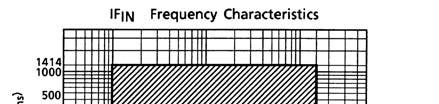
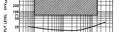
14 2. General-Purpose Counter Circuit Configuration TC9256, 57APG/AFG The general-purpose counter section consists of input amps, a gate time control circuit and a 20-bit binary counter. Figure 5 3. General-Purpose Counter Measurement Timing Frequency Measurement Timing Chart Cycle Measurement Timing Chart 0 < T 1 < = 0.25 (µs), 0 < T 2 < = 1 (ms) Figure 6 Note1: Note2: IF IN1 and IF IN2 input have built-in amps. Connecting a capacitor permits low-amplitude operation. SC IN is configured for CMOS input; therefore input signals should be logic level. 14
15 General-Purpose I/O Ports TC9256, 57APG/AFG These LSIs feature general-purpose output and I/O ports that are controlled through the serial ports. Input/Output Form TC9256APG, TC9256AFG TC9257APG, TC9257AFG Input/Output Configuration Output ports Dedicated: 3 ports Maximum: 4 ports (1 port for CMOS output) Dedicated: 4 ports N-channel open-drain output I/O ports Maximum: 2 ports Dedicated: 1 port Maximum: 5 ports CMOS input/output 1. General-Purpose Output Ports (OT-1to OT-4) Pins OT-1to OT-4 are general-purpose dedicated output ports used for control signal output. They are configured for N-channel open-drain output and have an off withstanding voltage of 12 V. The data set in bits O1to O4 of the input register (D2H) are output in parallel from their corresponding dedicated output port pins OT-1to OT-4. The TC9256APG and TC9256AFG do not have the dedicated output port OT-4, but setting the input register (D2H) CLK (O4C) bit to 1 converts pin DO2 into an output port OT-4 (configured for CMOS output). The data set in bits O1to O4 of the input register (D2H) can also be read from the DATA pins as output register (D3H) serial data O1to O4. (1) TC9257APG and TC9257AFG (2) TC9256APG and TC9256AFG Note 1: Bit names in parentheses ( ) apply to the TC9256APG and TC9256AFG. Note 2: (*1) indicates the output state when the DO2/OT-4 pin is switched for use as an OT-4 output pin (configured for CMOS output). 15
16 (3) Output register... The data set in bits O1 to O4 of the input register can be read as serial data O1 to O4 from the output register (D3H). 2. General-Purpose I/O Ports (I/O-5 to I/O-9) Pins I/O-5 to I/O-9 are general-purpose I/O ports used for control signal input and output. They are configured for CMOS input and output. These I/O ports are set for input or output using bits C5, C6 and M7 to M9 of the input register (D2H). Setting bits C5, C6 and M7 to M9 to 0 sets these ports for input. Data input in parallel from I/O-5to I/O-9 are latched in the internal register at the ninth falling edge of the serial clock signal. The data can then be read as serial data I5 to I9 from the DATA pins. Setting bits C5, C6 and M7 to M9 to 1 sets these ports for output. Data set in bits O5 to O9 of the input register (D2H) is output in parallel from their corresponding general-purpose I/O port pins I/O-5 to I/O-9. These operations are valid when bits SC, IF1, IF2 and CLK are all set to 0. (1) TC9257APG and TC9257AFG Setting data for output ports Note1: Note2: Note3: On TC9257APG and TC9257AFG, pins I/O-7to I/O-9 also serve as general-purpose counter input pins. Therefore, bits SC, IF1 and IF2 of the input register (D2H) must be set to 0 when pins I/O-7to I/O-9 are used for I/O ports. Since pin I/O-5 also serves as the CLK pin, the CLK bit of the input register (D2H) must be set to 0 when pin I/O-5 is used as an I/O port. Bit names in parentheses ( ) apply to the TC9256APG and TC9256AFG. Bits marked with (*1) cannot be set on the TC9256APG and TC9256AFG. 16
17 (2) TC9256APG and TC9256AFG Setting data for output ports (3) Output register... Data set in bits C5, C6 and M7to M9 of the input register (D2H) can be read as serial data C5, C6 and M7to M9 from the output register (D3H). Data input in parallel from pins I/O-5 to I/O-9 can be read as serial data I5 to I9 from the output register (D3H). 17
18 Note1: Note2: Bit names in parentheses ( ) apply to the TC9256APG and TC9256AFG. Bits marked with (*1) cannot be set on the TC9256APG and TC9256AFG. Data is 0 for bits marked with (*2) on the TC9256APG and TC9256AFG. Note3: Note4: When pins I/O-5 to I/O-9 are used for output, the data in I5~I9 of the output register (D3H) is undefined. When power is turned on, input register (D2H) I/O port control bits C5, C6 and M7 to M9 and output data bits O5 to O9 are set to 0. (General-purpose I/O ports are set as input ports. Pins used both as general-purpose I/O ports and general-purpose counter input are set for I/O port input. The output state of general-purpose output ports is set to high impedance (N-channel open drain output = off). Note5: On TC9256APG and TC9256AFG, pins I/O-5 and I/O-6 also serve as general-purpose counter input pins. Therefore, bits IF1 and IF2 of input register 2 must be set to 0 when these pins are used as I/O ports. A typical example of data setting for general-purpose counter and I/O port use is shown below. TC9257APG and TC9257AFG As shown above, the pins can be switched as required to enable use as an I/O port or general-purpose counter. 18
19 Phase Comparator TC9256, 57APG/AFG The phase comparator outputs the phase error after comparing the phase difference of the reference frequency signal supplied by the reference counter and the divided output from the programmable counter. The frequencies and phase differences of these two signals are then equalized by passing them through low-pass filters. These signals then control the VCOs. The filter constants can be customized for FM and AM bands since the signals are output in parallel from the phase comparator then pass through the two tristate buffer pins, DO1 and DO2. Figure 7 Figure 8 DO Output Timing Chart Figure 9 Typical Active Low-Pass Filter Circuit The figures above show the DO output timing chart and a typical active low-pass filter circuit featuring a Darlington connection between the FET and transistor. The filter circuit shown above is just one example. Actual circuits should be designed based on the band composition and the properties desired from the system. Note: On the TC9256APG and TC9256AFG, pin DO2 can be switched for use as pin OT-4. 19
20 Lock Detection Bits TC9256, 57APG/AFG The lock detection bits detect locked states in the PLL system. These systems have an unlock detection bit (unlock bit), which is used to detect, using the reference frequency cycle, the phase difference between the reference frequency and the divided output of the programmable counter. These systems also have phase error detection bits (bits PE1to PE3), which are capable of more precise detection (±0.55 µs to ±7.15 µs). 1. Unlock Detection Bit (UNLOCK) This bit detects, using the reference frequency cycle, the phase difference between the reference frequency and the divided output of the programmable counter. When there is no lock, that is, when the reference frequency and the divided output of the programmable counter are not the same, unlock F/F is set. Unlock F/F is reset every time the input register (D2H) unlock reset bit (RESET) is set to 1. After unlock F/F has been reset in this way, locked state can be detected by checking the unlock detection bit (UNLOCK) of the output register (D3H). After unlock F/F has been reset, the unlock detection bit must be checked after a time interval exceeding the reference frequency cycle. This is because the reference frequency cycle inputs the lock detection strobe to unlock F/F. If the time interval is short, the correct locked state cannot be detected. Therefore, the output register (D3H) has a lock enable bit (ENABLE). This bit is reset every time the input register (D2H) reset bit is set to 1, and set to 1 through the lock detection timing. That is, the locked state is correctly detected when the lock enable bit (ENABLE) is 1. Figure 10 20
21 Note: The asterisk (*) indicates an error state of over 180 phase difference relative to the reference frequency. 2. Phase Error Detection Bits (PE1to PE3) The unlock bit detects, using the reference frequency cycle, the phase difference between the reference frequency and the divided output of the programmable counter. The phase error detection bits (bits PE1to PE3) are capable of precise phase error detection of ±0.55 to ±7.15 µs using the reference frequency cycle. (If the UNLOCK bit is set to 1 and the phase difference relative to the reference frequency is over 180, bits PE1 to PE3 cannot correctly detect the phase error. Therefore, bits PE1to PE3 are normally used when the UNLOCK bit is set to 0.) Bits PE1to PE3 detects phase error normally when the phase difference is 180 to 180 relative to the reference frequency cycle. The phase error data can be read from the output register (D3H) as serial data PE1 to PE3. 21
22 The following is a typical lock detection operation. It shows the operation flow from locked state to frequency change with a phase error greater than ±4.95 µs and less than ±6.05 µs. Figure 11 22
23 Other Control Bits 1. CLK (O4C) and C5 (XT) Bits... Control bits that switch the function for the I/O-5/CLK pin on the TC9257APG and TC9257AFG, and the OT-4/DO2 pin on the TC9256APG and TC9256AFG. (1) On the TC9257APG and TC9257AFG, the CLK bit controls switching of the I/O-5 pin and CLK pin. When bits R0 to R3 of the input register (D0H) are all set to 1 (standby mode) When one of bits R0 to R3 of the input register (D0H) is set to 0 (not standby mode) Note1: The system clock output marked with an asterisk (*) refers to output of the crystal oscillator frequencies listed below. Crystal Oscillator (MHz) System Clock (khz) Duty (%) Note2: Bit names in parentheses ( ) apply to the TC9256APG and TC9256AFG. 23
24 (2) On the TC9256APG and TC9256AFG, the O4C bit controls switching of the DO2 pin and OT-4 pin. When bits R0 to R3 of the input register (D0H) are all set to 1 (standby mode) When one of bits R0 to R3 of the input register (D0H) is set to 0 (not standby mode) 2. DOHZ Bit... Controls the DO2 pin output state. 3. TEST Bit... Data should normally be set to 0. Note: Bit names in parentheses ( ) apply to the TC9256APG and TC9256AFG. 24
25 Absolute Maximum Ratings (Ta = 25 C) Characteristic Symbol Rating Unit Supply voltage V DD 0.3~6.0 V Input voltage V IN 0.3~V DD V N-ch open-drain OFF withstanding voltage V OFF 13 V Power dissipation P D 300 (200) mw Operating temperature T opr 40~85 C Storage temperature T stg 65~150 C ( ): Flat package Electrical Characteristics (unless otherwise specified, Ta = 40 to 85 C, V DD = 4.5 to5.5 V) Characteristic Symbol Test Circuit Operating power supply voltage V DD1 Operating power supply current I DD1 Test Condition Min Typ Max Unit PLL operation (normaloperation) V DD = 5.0 V, XT = 10.8 MHz, FM IN = 150 MHz V 7 15 ma Standby mode Characteristic Crystal oscillation frequency supply voltage Symbol V DD2 Test Circuit Operating power supply current I DD2 Operating power supply current I DD3 Test Condition Min Typ Max Unit PLL OFF (operating crystal oscillation) VDD = 5.0 V, XT = 10.8 MHz, PLL OFF VDD = 5.0 V, XT stop, PLL OFF V ma µa Operating frequency range Characteristic Symbol Test Circuit Test Condition Min Typ Max Unit Crystal oscillation frequency f XT Connect crystal resonator to XT- XT pin 3.6 ~ 10.8 MHz FM IN (FM H, FM L ) f FM FM H, FM L mode, V IN = 0.2 V p-p 30 ~ 130 MHz FM IN (FM L ) f FML FM L mode, V IN = 0.3 V p-p 30 ~ 150 MHz AM IN (HF) f HF HF mode, V IN = 0.2 V p-p 1 ~ 40 MHz AM IN (LF) f LF LF mode, V IN = 0.2 V p-p 0.5 ~ 20 MHz IF IN1, IF IN2 f IF V IN = 0.2 V p-p 0.1 ~ 15 MHz SC IN f SC V IH = 0.7 V DD, V IL = 0.3 V DD, Square wave input ~ 100 khz 25
26 Operating input amplitude range Characteristic Symbol Test Circuit FM IN (FM H, FM L ) V FM FM IN (FM L ) V FML Test Condition Min Typ Max Unit FM H, FM L mode, f IN = 30 to 130 MHz FM L mode, f IN = 30 to 150 MHz 0.2 ~ 0.3 ~ AM IN (HF) V HF HF mode, f IN = 1 to 40 MHz 0.2 ~ AM IN (LF) V LF LF mode, f IN = 0.5 to 20 MHz 0.2 ~ IF IN1, IF IN2 V IF f IN = 0.1 to 15 MHz 0.2 ~ V DD 0.5 V DD 0.5 V DD 0.5 V DD 0.5 V DD 0.5 V p-p V p-p V p-p V p-p V p-p OT1 to OT4 N-ch open drain Characteristic Symbol Test Circuit Test Condition Min Typ Max Unit Output current L level I OL1 V OL = 1.0 V ma OFF-leak current I OFF V OFF = 12 V 2.0 µa I/O-5 to I/O-9, SC IN Input voltage Input current Output current Characteristic Symbol Test Circuit H level V IH1 L level V IL1 Test Condition Min Typ Max Unit 0.7 V DD 0 ~ ~ V DD 0.3 V DD H level I IH V IH = 5 V 2.0 L level I IL V IL = 0 V 2.0 H level I OH4 V OH = 4.0 V (except SC IN ) L level I OL4 V OL = 1.0 V (except SC IN ) V µa ma PERIOD, CLOCK, DATA Input voltage Input current Output current Characteristic Symbol Test Circuit H level V IH2 L level V IL2 Test Condition Min Typ Max Unit 0.8 V DD 0 ~ ~ V DD 0.2 V DD H level I IH V IH = 5 V 2.0 L level I IL V IL = 0 V 2.0 H level I OH5 V OH = 4.0 V (DATA) L level I OL5 V OL = 1.0 V (DATA) V µa ma 26
27 DO1, DO2 Input current Characteristic Symbol Test Circuit Test Condition Min Typ Max Unit H level I OH3 V OH = 4.0 V L level I OL3 V OL = 1.0 V Tristate lead current I TL V TLH = 5 V, V TLL = 0 V ±1.0 µa ma XT Output current Characteristic Symbol Test Circuit Test Condition Min Typ Max Unit H level I OH2 V OH = 4.0 V L level I OL2 V OL = 1.0 V ma Input feedback resistance Characteristic Input feedback resistance Symbol Test Circuit Test Condition Min Typ Max Unit Rf1 FM IN, AM IN, IF IN (Ta = 25 C) Rf2 XT- XT (Ta = 25 C) kω 27


28 28
29 Application Circuit (Sample circuit containing TC9257APG and TC9257AFG) 29
30 Package Dimensions Weight: 1.0 g (typ.) (Note): Palladium plate 30
31 Package Dimensions Weight: 1.24 g (typ.) (Note): Palladium plate 31
32 Package Dimensions P-SOP A Unit : mm Weight: 0.16 g (typ.) (Note): Palladium plate 32
33 Package Dimensions P-SOP A Unit : mm Weight: 0.48 g (typ.) (Note): Palladium plate 33
34 RESTRICTIONS ON PRODUCT USE EBA The information contained herein is subject to change without notice _D TOSHIBA is continually working to improve the quality and reliability of its products. Nevertheless, semiconductor devices in general can malfunction or fail due to their inherent electrical sensitivity and vulnerability to physical stress. It is the responsibility of the buyer, when utilizing TOSHIBA products, to comply with the standards of safety in making a safe design for the entire system, and to avoid situations in which a malfunction or failure of such TOSHIBA products could cause loss of human life, bodily injury or damage to property. In developing your designs, please ensure that TOSHIBA products are used within specified operating ranges as set forth in the most recent TOSHIBA products specifications. Also, please keep in mind the precautions and conditions set forth in the Handling Guide for Semiconductor Devices, or TOSHIBA Semiconductor Reliability Handbook etc _A The TOSHIBA products listed in this document are intended for usage in general electronics applications (computer, personal equipment, office equipment, measuring equipment, industrial robotics, domestic appliances, etc.). These TOSHIBA products are neither intended nor warranted for usage in equipment that requires extraordinarily high quality and/or reliability or a malfunction or failure of which may cause loss of human life or bodily injury ( Unintended Usage ). Unintended Usage include atomic energy control instruments, airplane or spaceship instruments, transportation instruments, traffic signal instruments, combustion control instruments, medical instruments, all types of safety devices, etc. Unintended Usage of TOSHIBA products listed in this document shall be made at the customer s own risk _B The products described in this document shall not be used or embedded to any downstream products of which manufacture, use and/or sale are prohibited under any applicable laws and regulations _Q The information contained herein is presented only as a guide for the applications of our products. No responsibility is assumed by TOSHIBA for any infringements of patents or other rights of the third parties which may result from its use. No license is granted by implication or otherwise under any patent or patent rights of TOSHIBA or others _C The products described in this document are subject to the foreign exchange and foreign trade laws _E About solderability, following conditions were confirmed Solderability (1) Use of Sn-37Pb solder Bath solder bath temperature = 230 C dipping time = 5 seconds the number of times = once use of R-type flux (2) Use of Sn-3.0Ag-0.5Cu solder Bath solder bath temperature = 245 C dipping time = 5 seconds the number of times = once use of R-type flux 34
TR1002. PLL for DTS IC. Data Sheet
 TR1002 PLL for DTS IC Data Sheet tenx reserves the right to change or discontinue the manual and online documentation to this product herein to improve reliability, function or design without further notice.
TD6127BP TD6127BP. ECL Prescaller For Communications Radio. Features TOSHIBA Bipolar Digital Integrated Circuit Silicon Monolithic
 TOSHIBA Bipolar Digital Integrated Circuit Silicon Monolithic TD6127BP ECL Prescaller For Communications Radio TD6127BP is a 2 modulus prescaller developed for communications radio of PLL frequency synthesizer
TD62384APG,TD62384AFG TD62385APG,TD62385AFG
 TOSHIBA BIPOLAR DIGITAL INTEGRATED CIRCUIT SILICON MONOLITHIC TD62384APG,TD62384AFG TD62385APG,TD62385AFG 8CH LOW INPUT ACTIVE DARLINGTON SINK DRIVER The TD62384APG / AFG and TD62385APG / AFG are non inverting
TD62M8600FG TD62M8600FG 8CH LOW SATURATION VOLTAGE SOURCE DRIVER FEATURES SCHEMATICS PIN CONNECTION (TOP VIEW)
") TOSHIBA BIPOLAR DIGITAL INTEGRATED CIRCUIT MULTI CHIP TD62M8600FG TD62M8600FG 8CH LOW SATURATION VOLTAGE SOURCE DRIVER TD62M8600FG is Multi Chip IC incorporates 8 low saturation discrete transistors equipped
TOSHIBA BIPOLAR DIGITAL INTEGRATED CIRCUIT MULTI CHIP TD62M8600FG TD62M8600FG 8CH LOW SATURATION VOLTAGE SOURCE DRIVER TD62M8600FG is Multi Chip IC incorporates 8 low saturation discrete transistors equipped
TD62382AP,TD62382AF TD62382AP/AF 8CH LOW INPUT ACTIVE SINK DRIVER FEATURES PIN CONNECTION (TOP VIEW) SCHEMATICS (EACH DRIVER)
 SCHEMATICS (EACH DRIVER)") TOSHIBA BIPOLAR DIGITAL INTEGRATED CIRCUIT SILICON MONOLITHIC TD62382AP,TD62382AF TD62382AP/AF 8CH LOW INPUT ACTIVE SINK DRIVER The TD62382AP / AF are non inverting transistor array which are comprised
TOSHIBA BIPOLAR DIGITAL INTEGRATED CIRCUIT SILICON MONOLITHIC TD62382AP,TD62382AF TD62382AP/AF 8CH LOW INPUT ACTIVE SINK DRIVER The TD62382AP / AF are non inverting transistor array which are comprised
2SK117 2SK117. Low Noise Audio Amplifier Applications. Maximum Ratings (Ta 25 C) Electrical Characteristics (Ta 25 C)
 Electrical Characteristics (Ta 25 C)") TOSHIBA Field Effect Transistor Silicon N Channel Junction Type Low Noise Audio Amplifier Applications Unit: mm High Yfs : Yfs = 15 ms (typ.) (VDS = 10 V, VGS = 0) High breakdown voltage: VGDS = 50 V Low
TOSHIBA Field Effect Transistor Silicon N Channel Junction Type Low Noise Audio Amplifier Applications Unit: mm High Yfs : Yfs = 15 ms (typ.) (VDS = 10 V, VGS = 0) High breakdown voltage: VGDS = 50 V Low
1Z6.2~1Z390, 1Z6.8A~1Z30A
 TOSHIBA ZENER DIODE SILICON DIFFUSED JUNCTION TYPE 1Z6.2~1Z390, 1Z6.8A~A CONSTANT REGULATION TRANSIENT SUPPRESSORS Unit: mm Average Power Dissipation : P = 1 W Peak Reverse Power Dissipation : P RSM =
02DZ2.0~02DZ24 02DZ2.0~02DZ24. Constant Voltage Regulation Applications Reference Voltage Applications. Maximum Ratings (Ta = 25 C)
") TOSHIBA Diode Silicon Epitaxial Planar Type 02DZ2.0~02DZ24 Constant Voltage Regulation Applications Reference Voltage Applications Unit: mm The mounting of four devices on an ultra-compact package allows
TOSHIBA Diode Silicon Epitaxial Planar Type 02DZ2.0~02DZ24 Constant Voltage Regulation Applications Reference Voltage Applications Unit: mm The mounting of four devices on an ultra-compact package allows
CRY62~CRZ47 CRY62~CRZ47. Applications: Communication, Control and Measurement Equipment Constant Voltage Regulation Transient Suppressors
 TOSHIBA Zener Diode Silicon Epitaxial Type CRY62~CRZ47 Applications: Communication, Control and Equipment Constant Regulation Transient Suppressors Unit: mm Average power dissipation: P = 0.7 W Zener voltage:
02DZ2.0~02DZ24 02DZ2.0~02DZ24. Constant Voltage Regulation Applications Reference Voltage Applications. Absolute Maximum Ratings (Ta = 25 C)
") TOSHIBA Diode Silicon Epitaxial Planar Type 02DZ2.0~02DZ24 Constant Voltage Regulation Applications Reference Voltage Applications Unit: mm The mounting of four devices on an ultra-compact package allows
TOSHIBA Diode Silicon Epitaxial Planar Type 02DZ2.0~02DZ24 Constant Voltage Regulation Applications Reference Voltage Applications Unit: mm The mounting of four devices on an ultra-compact package allows
TORX147(F,T) TORX147(F,T) FIBER OPTIC RECEIVING MODULE FOR DIGITAL AUDIO INTERFACE. 1. Absolute Maximum Ratings (Ta = 25 C) 2.
 TORX147(F,T) FIBER OPTIC RECEIVING MODULE FOR DIGITAL AUDIO INTERFACE. 1. Absolute Maximum Ratings (Ta = 25 C) 2.") FIBER OPTIC RECEIVING MODULE TORX147(F,T) FIBER OPTIC RECEIVING MODULE FOR DIGITAL AUDIO INTERFACE Unit: mm For JEITA Standard CP 1212 (Digital Audio Optical Interface for Consumer Equipment). A self tapping
FIBER OPTIC RECEIVING MODULE TORX147(F,T) FIBER OPTIC RECEIVING MODULE FOR DIGITAL AUDIO INTERFACE Unit: mm For JEITA Standard CP 1212 (Digital Audio Optical Interface for Consumer Equipment). A self tapping
TORX176 TORX176 FIBER OPTIC RECEIVING MODULE FOR DIGITAL AUDIO EQUIPMENT. 1. Maximum Ratings (Ta = 25 C) 2. Recommended Operating Conditions
 2. Recommended Operating Conditions") FIBER OPTIC RECEIVING MODULE TORX176 FIBER OPTIC RECEIVING MODULE FOR DIGITAL AUDIO EQUIPMENT Unit: mm Conform to JEITA Standard CP 1201 (For Digital Audio Interfaces including Fiber Optic inter connections).
FIBER OPTIC RECEIVING MODULE TORX176 FIBER OPTIC RECEIVING MODULE FOR DIGITAL AUDIO EQUIPMENT Unit: mm Conform to JEITA Standard CP 1201 (For Digital Audio Interfaces including Fiber Optic inter connections).
TORX111 TORX111 FIBER OPTIC RECEIVING MODULE FOR APF. 1. Maximum Ratings (Ta = 25 C) FIBER OPTIC RECEIVING MODULE.
 FIBER OPTIC RECEIVING MODULE.") FIBER OPTIC RECEIVING MODULE TORX111 FIBER OPTIC RECEIVING MODULE FOR APF Unit: mm Non connector (connector less) type Data rate: DC to 6 Mb / s (NRZ code) Transmission distance: Up to 10 m (With TOTX111)
FIBER OPTIC RECEIVING MODULE TORX111 FIBER OPTIC RECEIVING MODULE FOR APF Unit: mm Non connector (connector less) type Data rate: DC to 6 Mb / s (NRZ code) Transmission distance: Up to 10 m (With TOTX111)
CRY62~CRZ47 CRY62~CRZ47. Use in Communication, Automation and Measurement Equipment Constant Voltage Regulation Transient Suppressors
 TOSHIBA Zener Diode Silicon Epitaxial Type CRY62~CRZ47 Use in Communication, Automation and Equipment Constant Regulation Transient Suppressors Unit: mm Average power dissipation: P = 0.7 W Zener voltage:
TLPGE183P TLPGE183P. Panel Circuit Indicator. Maximum Ratings (Ta = 25 C) TOSHIBA LED Lamp InGaAlP Pure Green Light Emission.
 TOSHIBA LED Lamp InGaAlP Pure Green Light Emission.") TLPGE8P TOSHIBA LED Lamp InGaAlP Pure Green Light Emission TLPGE8P Panel Circuit Indicator Unit in mm 5mm diameter(t /4) InGaAlP pure green LED All plastic mold type. Colorless clear lens Low drive current,high
TLPGE8P TOSHIBA LED Lamp InGaAlP Pure Green Light Emission TLPGE8P Panel Circuit Indicator Unit in mm 5mm diameter(t /4) InGaAlP pure green LED All plastic mold type. Colorless clear lens Low drive current,high
TC4049BP,TC4049BF, TC4050BP,TC4050BF
 TOSHIBA CMOS Digital Integrated Circuit Silicon Monolithic TC4049BP,TC4049BF, TC400BP,TC400BF TC4049B Hex Buffer/Converter (inverting type) TC400B Hex Buffer/Converter (non-inverting type) TC4049BP, TC400BP
TORX177(F,T) TORX177(F,T) TENTATIVE FIBER OPTIC RECEIVING MODULE FOR DIGITAL AUDIO INTERFACE. 1. Maximum Ratings (Ta = 25 C)
 TORX177(F,T) TENTATIVE FIBER OPTIC RECEIVING MODULE FOR DIGITAL AUDIO INTERFACE. 1. Maximum Ratings (Ta = 25 C)") TENTATIVE FIBER OPTIC RECEIVING MODULE TORX177(F,T) FIBER OPTIC RECEIVING MODULE FOR DIGITAL AUDIO INTERFACE Unit: mm For JEITA Standard CP- 1212 (Digital Audio Optical Interface for Consumer Equipment).
TENTATIVE FIBER OPTIC RECEIVING MODULE TORX177(F,T) FIBER OPTIC RECEIVING MODULE FOR DIGITAL AUDIO INTERFACE Unit: mm For JEITA Standard CP- 1212 (Digital Audio Optical Interface for Consumer Equipment).
FIBER OPTIC TRANSMITTING MODULE TOTX147(F,T)
") FIBER OPTIC TRANSMITTING MODULE TOTX147(F,T) FIBER OPTIC TRANSMITTING MODULE FOR DIGITAL AUDIO EQUIPMENT Unit: mm Conforms to JEITA Standard CP 1212 (Digital Audio Optical Interface for Consumer Equipment).
FIBER OPTIC TRANSMITTING MODULE TOTX147(F,T) FIBER OPTIC TRANSMITTING MODULE FOR DIGITAL AUDIO EQUIPMENT Unit: mm Conforms to JEITA Standard CP 1212 (Digital Audio Optical Interface for Consumer Equipment).
TORX178B TORX178B FIBER OPTIC RECEIVING MODULE FOR DIGITAL AUDIO INTERFACE. 1. Maximum Ratings (Ta = 25 C) FIBER OPTIC RECEIVING MODULE
 FIBER OPTIC RECEIVING MODULE") FIBER OPTIC RECEIVING MODULE TORX178B FIBER OPTIC RECEIVING MODULE FOR DIGITAL AUDIO INTERFACE Unit: mm Conforms to EIAJ Standard CP 1201 (For Digital Audio Interface including Fiber Optic inter connections).
FIBER OPTIC RECEIVING MODULE TORX178B FIBER OPTIC RECEIVING MODULE FOR DIGITAL AUDIO INTERFACE Unit: mm Conforms to EIAJ Standard CP 1201 (For Digital Audio Interface including Fiber Optic inter connections).
TOSHIBA CMOS Digital Integrated Circuit Silicon Monolithic TC7SGU04FU IN A GND
 TOSHIBA CMOS Digital Integrated Circuit Silicon Monolithic TC7SGU04FU Inverter (Unbuffered) Features High output current : ±8 ma (min) at = 3 Super high speed operation : t pd = 1.9 ns (typ.) at = 3.3,
TLP350F TLP350F. Industrial Inverter Inverter for Air Conditioner IGBT/Power MOSFET Gate Drive IH(Induction Heating) Pin Configuration (top view)
 Pin Configuration (top view)") TLP350F Industrial Inverter Inverter for Air Conditioner IGBT/Power MOSFET Gate Drive IH(Induction Heating) TOSHIBA Photocoupler GaAlAs IRED + Photo IC TLP350F The TOSHIBA TLP350F consists of a GaAlAs
TLP350F Industrial Inverter Inverter for Air Conditioner IGBT/Power MOSFET Gate Drive IH(Induction Heating) TOSHIBA Photocoupler GaAlAs IRED + Photo IC TLP350F The TOSHIBA TLP350F consists of a GaAlAs
TOSHIBA Photo-interrupter Infrared LED + Phototransistor TLP1243(C8)
") TLP24(C8) Copiers, Printers and Fax Machines Air-conditioners Game Machines TOSHIBA Photo-interrupter Infrared LED + Phototransistor TLP24(C8) The TLP24 (C8) is a compact photointerrupter with a built-in
TLP24(C8) Copiers, Printers and Fax Machines Air-conditioners Game Machines TOSHIBA Photo-interrupter Infrared LED + Phototransistor TLP24(C8) The TLP24 (C8) is a compact photointerrupter with a built-in
BDE6A5.0D-2 BDE6A5.0D-2. Low Capacitance ESD Protection for High Speed Data
 BYD Microelectronics Co., Ltd. Low Capacitance ESD Protection for High Speed Data The Series is designed to protect high speed data lines from ESD. Its common anode design protects up to two separate I/O
TMP89FS60FG Sample Program. Rev 1.0 Dec. 2007
 TMP89FS60FG Sample Program Rev 1.0 Dec. 2007 This is sample software to help customers understand Toshiba microcontrollers and learn how to create programs when developing new products. You can download
TOSHIBA MOS DIGITAL INTEGRATED CIRCUIT SILICON GATE CMOS
 TENTATIVE TOSHIBA MOS DIGITAL INTEGRATED CIRCUIT SILICON GATE CMOS 1-GBIT (128M 8 BITS) CMOS NAND E 2 PROM DESCRIPTION The TH58100 is a single 3.3 V 1-Gbit (1,107,296,256) bit NAND Electrically Erasable
TBD62785APG, TBD62785AFWG
 TOSHIBA BiCD Integrated Circuit Silicon Monolithic TBD62785APG, TBD62785AFWG 8-ch low active source type DMOS transistor array TBD62785APG/FWG TBD62785A series product is a DMOS transistor array with 8
TD62783APG, TD62783AFWG
 TOSHIBA BIPOLAR DIGITAL INTEGRATED CIRCUIT SILICON MONOLITHIC 8CH HIGH VOLTAGE SOURCE DRIVER TD62783APG, TD62783AFWG The TD62783APG / AFWG are comprised of eight source current Transistor Array. These
TA75W393FU TA75W393FU. Dual Voltage Comparator. Features. Marking (Top View) Pin Connection (Top View)
 Pin Connection (Top View)") TOSHIBA Bipolar Linear Integrated Circuit Silicon Monolithic TA75W393FU Dual Voltage Comparator This device consist of two independent voltage comparators that designed to operate from a single power supply
TOSHIBA Bipolar Linear Integrated Circuit Silicon Monolithic TA75W393FU Dual Voltage Comparator This device consist of two independent voltage comparators that designed to operate from a single power supply
TOSHIBA Bi-CMOS Integrated Circuit Silicon Monolithic TB62781FNG
 TOSHIBA Bi-CMOS Integrated Circuit Silicon Monolithic TB62781FNG 9-Channel Current LED Driver of the 3.3V and 5V Power Supply Voltage Operation 1. Features Power supply voltages: V CC = 3.3 V/5 V Output
BDE2S5.0 BDE2S5.0. ESD Protection Diodes. In Ultra Small DFN1006-2L Package. Package Type DFN1006-2L
 BYD Microelectronics Co., Ltd. ESD Protection Diodes In Ultra Small DFN1006-2L Package The Series is designed to protect voltage sensitive components from damage due to ESD. Excellent clamping capability,
AF / 12. General Description. Features. Applications. Package. Pin. Configurations AF-V1.0. Analog Future
 16-channel constant current LED driver chip General Description The 5024 is a constant current driver chip which is designed for LED lighting and LED screen. The size of the drive urrent can be adjusted
TCS40DPR. Digital Output Magnetic Sensor. Feature. Marking Pin Assignment (Top View) Function Table PA8
 Function Table PA8") TOSHIBA CMOS Digital Integrated Circuit Silicon Monolithic TCS40DPR Digital Output Magnetic Sensor Feature Push-Pull Output South-Pole and North-Pole Detection Weight: 11.0 mg (typ.) SON3-P-0203-1.90S
TOSHIBA CMOS Digital Integrated Circuit Silicon Monolithic TCS40DPR Digital Output Magnetic Sensor Feature Push-Pull Output South-Pole and North-Pole Detection Weight: 11.0 mg (typ.) SON3-P-0203-1.90S
Power MOSFETs. Low Voltage High speed Series for DC-DC Converters. (synchronous converter) February 2005 TOSHIBA CORPORATION. Semiconductor Company
 February 2005 TOSHIBA CORPORATION. Semiconductor Company") 1 Power MOSFETs Low Voltage High speed Series for DC-DC Converters (synchronous converter) February 2005 TOSHIBA CORPORATION Semiconductor Company Discrete Semiconductor Division Load Sw PW MOS FET in
1 Power MOSFETs Low Voltage High speed Series for DC-DC Converters (synchronous converter) February 2005 TOSHIBA CORPORATION Semiconductor Company Discrete Semiconductor Division Load Sw PW MOS FET in
TOSHIBA CMOS Digital Integrated Circuit Silicon Monolithic TMPN3120FE5MG
 TOSHIBA CMOS Digital Integrated Circuit Silicon Monolithic TMPN3120FE5MG Neuron Chip for Distributed Intelligent Control Networks (LONWORKS ) TMPN3120FE5MG The TMPN3120FE5MG features extra single-chip
UNISONIC TECHNOLOGIES CO., LTD
 UNINIC TECHNOLOGIES CO., LTD 20-BIT SERIAL TO PARALLEL CONVERTER DESCRIPTION The UTC LS3718 is a 20-bit serial to parallel converter utilizing CMOS Technology. It is incorporates control circuit, shift
BDE6A5.0D-3 BDE6A5.0D-3. Low Capacitance ESD Protection for High Speed Data
 BYD Microelectronics Co., Ltd. Low Capacitance ESD Protection for High Speed Data The Series is designed to protect high speed data lines from ESD. Its common anode design protects up to four separate
TOSHIBA CMOS Digital Integrated Circuit Silicon Monolithic TMPN3120FE3MG
 TOSHIBA CMOS Digital Integrated Circuit Silicon Monolithic TMPN3120FE3MG Neuron Chip for Distributed Intelligent Control Networks (LONWORKS ) TMPN3120FE3MG The TMPN3120FE3MG features extra single-chip
LC75700T. Key Scan IC. Package Dimensions. Overview. Features CMOS IC
 Ordering number : ENN7632 CMOS IC LC75700T Key Scan IC Overview The LC75700T is a key scanning LSI that accepts input from up to 30 keys and can control up to four generalpurpose output ports. Therefore
unit: mm 3067-DIP24S unit: mm 3112-MFP24S
 Ordering number : EN4973A CMOS LSI AM/FM PLL Frequency Synthesizer Overview The LC72130 and LC72130M are PLL frequency synthesizers for use in tuners in radio cassette recorders and other products. Applications
LC75808E, 75808W. 1/8 to 1/10 Duty LCD Display Drivers with Key Input Function
 Ordering number : ENN6370A CMOS IC LC75808E, 75808W 1/8 to 1/10 Duty LCD Display Drivers with Key Input Function Overview The LC75808E and LC75808W are 1/8 to 1/10 duty LCD display drivers that can directly
LAPIS Semiconductor ML9298
 12-Hour System Clock IC for 1/2 Duty Fluorescent Display Tubes FEDL9298-01 Issue Date: Jul. 11, 2005 GENERAL DESCRIPTION The is a 12-hour system clock IC that drives 1/2 duty fluorescent display tubes.
Structure :Silicon Monolithic integrated circuit Product name :Voice Synthesis LSI Type :BU6939FV
 1/4 Structure :Silicon Monolithic integrated circuit Product name :Voice Synthesis LSI Type :BU6939FV Features 1) Single playback mode, Available bit-rate is 16kbps(High compression) - 128kbps(High Quarity)
LC72121, 72121M, 72121V
 Ordering number : EN5815A CMOS IC LC72121, 72121M, 72121V PLL Frequency Synthesizers for Electronic Tuning Overview The LC72121 and the LC72121M and the LC72121V are high input sensitivity (20 mvrms at
Operating temperature Topr 40 to +85 C Storage temperature Tstg 55 to +125 C
 Ordering number : EN3356A SANYO Semiconductors DATA SHEET LC7185-8750 Overview This 27 MHz band, PLL frequency synthesizer LSI chip is designed specifically for CB transceivers. The specifications are
LC79401KNE. CMOS LSI Dot-Matrix LCD Drivers. Ordering number : ENA1419
 Ordering number : ENA1419 COS LSI Dot-atrix LCD Drivers Overview The is a 80-outputs segment driver LSI for graphic dot-matrix liquid crystal display systems. The latches 80 bits of display data sent from
Features. General Description. Applications. Typical Application. QX5252 Solar LED Driver
 General Description QX5252 is an ASIC for solar LED lawn lights. Only a peripheral inductor is required to realize the step-up power supply, and the maximum drive efficiency can exceed 84%. QX5252 has
S-2900A. Rev CMOS 512-bit SERIAL E 2 PROM
 Rev.1.11 CMOS 512-bit SERIAL E 2 PROM S-29A The S-29A is a wide operating voltage range, low power consumption 512-bit E 2 PROM. The organization is 64-word 8-bit, and can be read or written serially.
TOSHIBA Schottky Barrier Rectifier Schottky Barrier Type CMS05
 CMS5 TOSHIBA Schottky Barrier Rectifier Schottky Barrier Type CMS5 Switching Mode Power Supply Applications Portable Equipment Battery Applications Unit: mm Repetitive peak reverse voltage : V RRM = 3
S-2900A. Rev.1.1. CMOS 512-bit SERIAL E 2 PROM
 Rev.1.1 CMOS 512-bit SERIAL E 2 PROM S-29A The S-29A is a wide operating voltage range, low power consumption 512-bit E 2 PROM. The organization is 64-word 8-bit, and can be read or written serially. It
LC79431KNE. CMOS LSI Dot-Matrix LCD Drivers. Ordering number : ENA2124
 Ordering number : ENA2124 COS LSI Dot-atrix LCD Drivers Overview The is a large-scale dot matrix LCD common driver LSI. The contains an 80-bit bidirectional shift register and is equipped with a 4-level
RN1601, RN1602, RN1603 RN1604, RN1605, RN1606
 TOSHIBA Transistor Silicon NPN Epitaxial Type (PCT Process) (Bias Resistor built-in Transistor) Switching, Inverter Circuit, Interface Circuit and Driver Circuit Applications RN1601, RN1602, RN1603 RN1604,
Drawing code Package Tape Reel 8-Pin DIP DP008-F 8-Pin SOP(JEDEC) FJ008-A FJ008-D FJ008-D 8-Pin TSSOP FT008-A FT008-E FT008-E
 FJ008-A FJ008-D FJ008-D 8-Pin TSSOP FT008-A FT008-E FT008-E") Rev. 3.2_ CMOS SERIAL E 2 PROM Features The is a high speed, low current consumption, 8 K-bit serial E 2 PROM with a wide operating voltage range. It is organized as 512-word 16-bit respectively. Each
Rev. 3.2_ CMOS SERIAL E 2 PROM Features The is a high speed, low current consumption, 8 K-bit serial E 2 PROM with a wide operating voltage range. It is organized as 512-word 16-bit respectively. Each
S-24 Series. Rev.1.1 SERIAL NON-VOLATILE RAM
 Rev.. SERIL NON-VOLTILE RM S- Series The S- Series is a non-volatile CMOS RM, composed of a CMOS static RM and a non-volatile electrically erasable and programmable memory (E PROM) to backup the SRM. The
3. Absolute Maximum Ratings (Note) (Unless otherwise specified, T a = 25 ) Symbol V ESD. P PK I PP T j T stg
 (Unless otherwise specified, T a = 25 ) Symbol V ESD. P PK I PP T j T stg") ESD Protection Diodes DF2B6M4SL Silicon Epitaxial Planar DF2B6M4SL 1. Applications ESD Protection This product is designed for protection against electrostatic discharge (ESD) and is not intended for any
ESD Protection Diodes DF2B6M4SL Silicon Epitaxial Planar DF2B6M4SL 1. Applications ESD Protection This product is designed for protection against electrostatic discharge (ESD) and is not intended for any
TCK22xxxG, TCK2065G, TCK1024G
 TOSHIBA CMOS Linear Integrated Circuit Silicon Monolithic TCK22xxxG, TCK2065G, TCK1024G Load Switch IC with Over current limited function The TCK22xxxG, TCK2065G and TCK1024G are Load Switch ICs for power
LC75700T/D. Key Scanning IC
 Key Scanning IC Overview The LC75700T is a key scanning LSI that accepts input from up to 30 keys and can control up to four general purpose output ports. Therefore it can reduce the number of lines to
DF10G7M1N DF10G7M1N. 1. Applications. 2. Packaging and Internal Circuit Rev.5.0. Start of commercial production
 ESD Protection Diodes DF10G7M1N Silicon Epitaxial Planar DF10G7M1N 1. Applications ESD Protection for: USB 2.0 USB 3.0 HDMI SATA/eSATA DisplayPort Interface Digital Visual Interface (DVI) MDDI PCI Express
TOSHIBA Schottky Barrier Diode CMS16
 CMS6 TOSHIBA Schottky Barrier Diode CMS6 Switching Mode Power Supply Applications Portable Equipment Battery Applications - Converter Applications Unit: mm Repetitive peak reverse voltage : VRRM = 4 V
DF2S6.8FS DF2S6.8FS. 1. Applications. 2. Packaging and Internal Circuit Rev.5.0. Start of commercial production.
 ESD Protection Diodes DF2S6.8FS Silicon Epitaxial Planar DF2S6.8FS 1. Applications ESD Protection This product is designed for protection against electrostatic discharge (ESD) and is not intended for any
ABLIC Inc., Rev.1.4_00
 www.ablicinc.com S-35720 Series FOR AUTOMOTIVE 125 C OPERATION WITH INTERRUPT TIME SETTING PIN CONVENIENCE TIMER ABLIC Inc., 2015-2018 Rev.1.4_00 The convenience timer is a CMOS timer IC which operates
1.8V/3.0V Single-PLL Clock Generator AK8150C
 AK8150C 1.8V/3.0V Single-PLL Clock Generator AK8150C Features Input Frequency: 38 MHz (1.8V or 3.0V) PLL Output Frequency: 12 MHz (1.8V or 3.0V) REF Output Frequency: 38 MHz or 19 MHz (1.8V or 3.0V) Low
TOSHIBA Zener Diode Silicon Epitaxial Type. CRY62 to CRZ39
 TOSHIBA Zener Diode Silicon Epitaxial Type CRY62 to CRZ39 Surge absorber Unit: mm Average power dissipation : P = 0.7 W Zener voltage : VZ = 6.2 to 39 V Suitable for compact assembly due to small surface-mount
DF2S16FS DF2S16FS. 1. Applications. 2. Packaging and Internal Circuit Rev Toshiba Corporation
 ESD Protection Diodes DF2S16FS Silicon Epitaxial Planar DF2S16FS 1. Applications ESD Protection Note: This product is designed for protection against electrostatic discharge (ESD) and is not intended for
1.8V/3.0V Single-PLL Clock Generator
 ASAHI KASEI EMD CORPORATION 1.8V/3.0V Single-PLL Clock Generator Features Input Frequency: 36 MHz (1.8V or 3.0V) PLL Output Frequency: 12 MHz (1.8V or 3.0V) REF Output Frequency: 36 MHz or 18 MHz (1.8V
TORX147PL(F,T) TORX147PL(F,T) FIBER OPTIC RECEIVING MODULE FOR DIGITAL AUDIO INTERFACE. 1. Absolute Maximum Ratings (Ta = 25 C) 2.
 TORX147PL(F,T) FIBER OPTIC RECEIVING MODULE FOR DIGITAL AUDIO INTERFACE. 1. Absolute Maximum Ratings (Ta = 25 C) 2.") FIBER OPTIC RECEIVING MODULE TORX147PL(F,T) FIBER OPTIC RECEIVING MODULE FOR DIGITAL AUDIO INTERFACE Unit: mm For JEITA Standard CP 1212 (Digital Audio Optical Interface for Consumer Equipment). Mini-package
FIBER OPTIC RECEIVING MODULE TORX147PL(F,T) FIBER OPTIC RECEIVING MODULE FOR DIGITAL AUDIO INTERFACE Unit: mm For JEITA Standard CP 1212 (Digital Audio Optical Interface for Consumer Equipment). Mini-package
DF2B6M4SL DF2B6M4SL. 1. General. 2. Applications. 3. Features. 4. Packaging Rev.4.0. Start of commercial production
 ESD Protection Diodes DF2B6M4SL Silicon Epitaxial Planar DF2B6M4SL 1. General The DF2B6M4SL is a TS diode (ESD protection diode) protects semiconductor devices used in mobile device interfaces and other
Dual PLL frequency synthesizer
 Dual PLL frequency synthesizer The BU2630F/BU2630FV are a CMOS LSI with an internal dual PLL synthesizer. VCOs for transmission and reception can be controlled independently, and the reference frequency
RN1101MFV,RN1102MFV,RN1103MFV RN1104MFV,RN1105MFV,RN1106MFV
 TOSHIBA Transistor Silicon NPN Epitaxial Type (PCT Process),,,, Switching, Inverter Circuit, Interface Circuit and Driver Circuit Applications z Ultra-small package, suited to very high density mounting
Dot Matrix LCD Controller Driver
 PF22-7 SED27F/D Dot Matrix LCD Controller Driver /, / or /6 Duty Dot Matrix Drive ROM 24 characters Built-in Character Generator ROM and RAM ( RAM characters ) Maximum Simultaneous Display of Characters
Small and Dynamic SD Card. An array of choices to store your important data and connect to a wide range of digital devices.
 Small and Dynamic SD Card An array of choices to store your important data and connect to a wide range of digital devices. The world for the SD Card is expanding Use of media cards continues to expand
S-29530A/29630A CMOS SERIAL E 2 PROM. Rev.1.2_00. Features. Packages
 Rev.1.2_ CMOS SERIAL E 2 PROM The S-2953A / 63A series are low power 16K / 32K-bit E 2 PROM with a low operating voltage range. They are organized as 124-word 16-bit and 248-word 16bit, respectively. Each
XRD87L85 Low-Voltage CMOS 8-Bit High-Speed Analog-to-Digital Converter
 Low-Voltage CMOS 8-Bit High-Speed Analog-to-Digital Converter April 2002-1 FEATURES 8-Bit Resolution Up to 10 MHz Sampling Rate Internal S/H Function Single Supply: 3.3V VIN DC Range: 0V to V DD VREF DC
中显液晶 技术资料 中显控制器使用说明书 2009年3月15日 北京市海淀区中关村大街32号和盛大厦811室 电话 86 010 52926620 传真 86 010 52926621 企业网站.zxlcd.com
 http://wwwzxlcdcom 4 SEG / 6 COM DRIVER & CONTROLLER FOR DOT MATRIX LCD June 2 Ver Contents in this document are subject to change without notice No part of this document may be reproduced or transmitted
Table 1 Brief Specifications
 Rev.1.1 MICROCOMPUTER WITH BUILT-IN PAGING DECODER The microcomputer incorporates a decoder conforming to CCIR Radio Paging Decode 1(POCSA Code), a melody generator, an LCD driver and a timer. Only attaching
S-2812A/2817A. Rev.1.1. CMOS 16K-bit PARALLEL E 2 PROM
 Rev.1.1 CMOS 16K-bit PARALLEL E 2 PROM The S-2812A and the S-2817A are low power 2K 8-bit parallel E 2 PROMs. The S-2812A features wide operating voltage range, and the S-2817A features 5-V single power
S-93C76A 3-WIRE SERIAL E 2 PROM. Features. Packages. ABLIC Inc., Rev.7.0_03
 www.ablicinc.com 3-WIRE SERIAL E 2 PROM ABLIC Inc., 21-215 Rev.7._3 The is a high speed, low current consumption, 3-wire serial E 2 PROM with a wide operating voltage range. The S- 93C76A has the capacity
16COM / 40SEG DRIVER & CONTROLLER FOR DOT MATRIX LCD
 INTRODUCTION KS0066U is a dot matrix LCD driver & controller LSI whichis fabricated by low power CMOS technology It can display 1or 2 lines with the 5 8 dots format or 1 line with the 5 11 dots format
UNISONIC TECHNOLOGIES CO., LTD 6621 Preliminary LINEAR INTEGRATED CIRCUIT
 UNISONIC TECHNOLOGIES CO., LTD 6621 Preliminary LINEAR INTEGRATED CIRCUIT RAM MAPPLING 32 4 LCD CONTROLLER FOR I/O μc DESCRIPTION The UTC 6621 is a 128 patterns (32 4), memory mapping, and multi-function
Two Outputs Clock Generator AK8146B
 ASAHI KASEI EMD CORPORATION Two Outputs Clock Generator AK8146B Features Pin Selectable External Input - 74.17582MHz - 74.25MHz - 60MHz Clock out Frequencies: - 12.000MHz - 13.5MHz Low Jitter Performance
UNISONIC TECHNOLOGIES CO.,LTD. UL318 Preliminary LINEAR INTEGRATED CIRCUIT
 UNISONIC TECHNOLOGIES CO.,LTD. UL318 Preliminary LINEAR INTEGRATED CIRCUIT SERIAL-INTERFACED 10-DIGIT LED CONTROLLER IC WITH KEYSCAN DESCRIPTION The UL318 is a compact LED controller and driver that interface
16COM/80SEG DRIVER & CONTROLLER FOR DOT MATRIX LCD
 6COM/80SEG DRIVER & CONTROLLER FOR DOT MATRIX LCD INTRODUCTION The is a dot matrix LCD driver & controller LSI which is fabricated by low power CMOS technology It is capable of displaying or 2 lines with
TC90195XBG Video signal Processing
 CMOS Digital Integrated Circuit Silicon Monolithic TC90195XBG Video signal Processing Overview TC90195XBG is a video signal processing LSI for the HD input and output. This device receives an analog video
TOSHIBA BIPOLAR LINEAR INTEGRATED CIRCUIT SILICON MONOLITHIC TA8428K, TA8428FG. Weight HSIP7 P 2.54 : 1.88 g (Typ.) The TA8428FG is RoHS compatible.
 The TA8428FG is RoHS compatible.") TOSHIBA BIPOLAR LINEAR INTEGRATED CIRCUIT SILICON MONOLITHIC TA8428K, DC MOTOR FULL-BRIDGE (H-BRIDGE) DRIVER ICs (Forward/reverse switching driver ICs) TA8428K/FG The TA8428K, is Full Bridge Driver IC
TOSHIBA BIPOLAR LINEAR INTEGRATED CIRCUIT SILICON MONOLITHIC TA8428K, DC MOTOR FULL-BRIDGE (H-BRIDGE) DRIVER ICs (Forward/reverse switching driver ICs) TA8428K/FG The TA8428K, is Full Bridge Driver IC
XRD8775 CMOS 8-Bit High Speed Analog-to-Digital Converter
 CMOS 8-Bit High Speed Analog-to-Digital Converter April 2002-4 FEATURES 8-Bit Resolution Up to 20MHz Sampling Rate Internal S/H Function Single Supply: 5V V IN DC Range: 0V to V DD V REF DC Range: 1V to
16COM/40SEG DRIVER & CONTROLLER FOR DOT MATRIX LCD
 6COM/4SEG DRIVER & CONTROLLER FOR DOT MATRIX LCD INTRODUCTION is a dot matrix LCD driver & controller LSI which is fabricated by low power CMOS technology It can display, 2-line with 5 x 8 or 5 x dots
SII Semiconductor Corporation, 2017 Rev.1.1_00
 www.sii-ic.com FOR AUTOMOTIVE 125 C OPERATION 2-WIRE BUILT-IN QUARTZ CRYSTAL CONVENIENCE TIMER SII Semiconductor Corporation, 217 The convenience timer is a CMOS timer IC which operates with low current
HT1621. RAM Mapping 32 4 LCD Controller for I/O µc. Features. General Description. Selection Table
 RAM Mapping 32 4 LCD Controller for I/O µc Features Operating voltage : 2.4V~5.2V Built-in 256kHz RC oscillator External 32.768kHz crystal or 256kHz frequency source input Selection of 1/2 or 1/3 bias,
TBD62783APG, TBD62783AFG, TBD62783AFNG, TBD62783AFWG
 TOSHIBA BiCD Integrated Circuit Silicon Monolithic TBD62783APG/FG/FNG/FWG TBD62783APG, TBD62783AFG, TBD62783AFNG, TBD62783AFWG 8channel source type DMOS transistor array TBD62783A series are DMOS transistor
TBD62308AFAG TBD62308AFAG. TOSHIBA BiCD Integrated Circuit Silicon Monolithic. 4channel Low active high current sink type DMOS transistor array
 TOSHIBA BiCD Integrated Circuit Silicon Monolithic TBD62308AFAG 4channel Low active high current sink type DMOS transistor array TBD62308AFAG are DMOS transistor array with 4 circuits. It has a clamp diode
Register Programmable Clock Generator AK8141
 ASAHI KASEI EMD CORPORATION Register Programmable Clock Generator Features Input Frequency: 48MHz/24MHz/12MHz/27MHz (Selectable) Output Frequency: 27MHz 50MHz by 1MHz step, 33.75MHz/40.5MHz/49.5MHz (Selectable)
ABLIC Inc., Rev.1.6_00
 S-35710 Series www.ablicinc.com FOR AUTOMOTIVE 125 C OPERATION 2-WIRE CONVENIENCE TIMER ABLIC Inc., 2014-2018 Rev.1.6_00 The convenience timer is a CMOS timer IC which operates with low current consumption,
Semiconductor MSM6442 GENERAL DESCRIPTION FEATURES E2E This version: Sep. MSM Previous version: Mar. 1996
 E2E0017-38-93 Semiconductor Semiconductor Built-in LCD Driver 4-Bit Microcontroller This version: Sep. 1998 Previous version: Mar. 1996 GENERAL DESCRIPTION The is a 4-bit microcontroller with a built-in
UNISONIC TECHNOLOGIES CO., LTD US2005 Preliminary CMOS IC
 UNISONIC TECHNOLOGIES CO., LTD US2005 Preliminary CMOS IC FIXED CURRENT LIMIT POWER DISTRIBUTION SWITCH DESCRIPTION UTC US2005 is a low voltage cost-effective high-side power switch with current limiting
LE2416RLBXA. Overview. Functions. CMOS IC Two Wire Serial InterfaceEEPROM (16k EEPROM)
") Ordering number : ENA2070 LE2416RLBXA CMOS IC Two Wire Serial InterfaceEEPROM (16k EEPROM) http://onsemi.com Overview The LE2416RLBXA is a 2-wire serial interface EEPROM. It realizes high speed and a high
Ordering number : ENA2070 LE2416RLBXA CMOS IC Two Wire Serial InterfaceEEPROM (16k EEPROM) http://onsemi.com Overview The LE2416RLBXA is a 2-wire serial interface EEPROM. It realizes high speed and a high
16COM / 80SEG DRIVER & CONTROLLER FOR DOT MATRIX LCD
 INTRODUCTION KS0070B is a dot matrix LCD driver & controller LSI which is fabricated by low power CMOS technology. It is capable of displaying 1 or 2 lines with the 5 7 format or 1 line with the 5 10 dots
Preliminary Data MOS IC. Type Ordering Code Package SDA Q67100-H5092 P-DIP-8-1
 Nonvolatile Memory 1-Kbit E 2 PROM SDA 2516-5 Preliminary Data MOS IC Features Word-organized reprogrammable nonvolatile memory in n-channel floating-gate technology (E 2 PROM) 128 8-bit organization Supply
INTEGRATED CIRCUITS. PCA bit I 2 C and SMBus I/0 port with reset. Product data Supersedes data of 2002 May Dec 13
 INTEGRATED CIRCUITS Supersedes data of 2002 May 13 2002 Dec 13 Philips Semiconductors FEATURES Lower voltage, higher performance migration path for the PCA9556 8 general purpose input/output expander/collector
NJU Digital Signal Processor for TV. General Description
 Digital Signal Processor for TV General Description The NJU26124 is a high performance 24-bit digital signal processor. The NJU26124 provides 512TAP FIR Filter, and. These kinds of sound functions are
LE24L042CS-B. Overview. Functions. CMOS IC Two Wire Serial Interface EEPROM (4k EEPROM)
") Ordering number : ENA2068 CMOS IC Two Wire Serial Interface EEPROM (4k EEPROM) http://onsemi.com Overview The is a 2-wire serial interface EEPROM. It realizes high speed and a high level reliability by
Ordering number : ENA2068 CMOS IC Two Wire Serial Interface EEPROM (4k EEPROM) http://onsemi.com Overview The is a 2-wire serial interface EEPROM. It realizes high speed and a high level reliability by
NTE1731 Integrated Circuit CMOS 10 Number Pulse Dialer
 NTE1731 Integrated Circuit CMOS 10 Number Pulse Dialer Description: The NTE1731 is a CMOS LSI repertory dialer with ten 16 digit number memory storage in a 16 Lead DIP type package. The pulse and mute