Features. Applications
|
|
|
- Ronald Small
- 5 years ago
- Views:
Transcription
1 Push-Button Reset IC General Description The are low-current, ultra-small, pushbutton reset supervisors with long set-up delays. The devices feature two manual reset inputs and two reset outputs. The devices initiate a reset for the reset timeout period when the /MR0 and /MR1 inputs are asserted low for a period longer than the set-up delay. The two manual reset inputs and long set-up period help to avoid unintended system resets. Both manual reset inputs can be tied together if a single push-button reset is desired. The MIC2788 features integrated pull-up resistors on the /MR0 and /MR1 inputs, while the MIC2789 requires external pull-up resistors. The PDY input pin selects between a 2s, 4s or 6s set-up period. Factory-programmed reset timeout periods of 140ms (min.) and 240ms (min.) are available. An active-low, open-drain reset output (/RST) and an active-high, push-pull reset output (RSTP) provide flexibility when interfacing to various microcontrollers, PMICs, or load switches. The consume a quiescent current of only 2.9µA and are offered in a tiny, space-saving 8-pin thin MLF (2mm x 2mm x 0.55mm) package. Data sheets and support documentation can be found on Micrel s web site at: Features 1.6V to 5.5V operating voltage 2.9µA supply current when /MR0, /MR1 are not asserted Asserting /MR0 and /MR1 for longer than set-up delay asserts reset output for the reset timeout period Programmable delay (PDY) input selects 2.0s, 4.0s or 6.0s set-up delay Factory-programmed 140ms (min.) or 240ms (min.) reset timeout period Integrated /MR0, /MR1 pull-up resistors (MIC2788) Dual Reset Outputs: Open-drain active-low reset (/RST) output Push-pull active-high reset (RSTP) output 40 C to 85 C ambient operating temperature range 8-pin 2mm x 2mm x 0.55mm thin MLF package Applications Smart phones MP3 players Portable navigation devices Set-top boxes (STBs) Tablets/pads Typical Application MLF and MicroLeadFrame are registered trademarks of Amkor Technologies, Inc. Micrel Inc Fortune Drive San Jose, CA USA tel +1 (408) fax + 1 (408) October 2011 M A
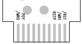
2 Ordering Information (1) Part Number Marking Minimum t RESET (ms) Package (3,4) Integrated Pull-Up Resistors MIC2788-XYMT 8XA Pin (2mm 2mm) Thin MLF Yes MIC2788-YYMT (2) 8YA Pin (2mm 2mm) Thin MLF Yes MIC2789-XYMT 9XA Pin (2mm 2mm) Thin MLF No MIC2789-YYMT (2) 9YA Pin (2mm 2mm) Thin MLF No Notes: 1. All devices available in Tape and Reel only. 2. Contact factory for availability. 3. Thin MLF = Pin 1 identifier. 4. Thin MLF is a Green RoHS compliant package. Lead finish is NiPdAu. Mold compound is Halogen Free. Pin Configuration MIC2788/89 8-Pin (2mm 2mm) Thin MLF Top View Pin Description Pin Number Pin Name Pin Function 1 RSTP Active-High Push-Pull Reset Output. This output changes from low-to-high when both manual reset pins are pulled low for the setup delay period. RSTP remains high for the reset timeout delay duration after the setup delay period has elapsed. 2 GND Supply Ground. 3 /MR1 Active-Low Manual Reset Input. The MIC2788 has an internal 65kΩ pull-up resistor to VIN while the MIC2789 requires an external pull-up resistor to VIN if used with a push-button. Pull this pin low to assert and force a reset. Pulling both manual reset inputs low for the setup delay time causes one reset output pulse for the reset timeout delay period. Connect to VIN if unused, do not leave floating. 4 /RST Active-Low Open Drain Reset Output. This output changes from high to low when both manual reset pins are pulled low for the setup delay period. /RST remains low for the reset timeout delay after the setup delay has elapsed and it requires an external pull-up resistor. 5 PDY Programmable Delay Input with Tri-State Connection. When left open, set-up delay is 2s, when connected to GND, set-up delay is 4s and when connected to VIN, set-up delay is 6s. October M A
3 Pin Description (Continued) Pin Number Pin Name Pin Function 6 NC No Connect. Leave pin floating. 7 /MR0 8 VIN Active-Low Manual Reset Input. The MIC2788 has an internal 65kΩ pull-up resistor to VIN while the MIC2789 requires an external pull-up resistor to VIN if used with a push-button. Pull this pin low to assert and force a reset. Pulling both manual reset inputs low for the setup delay time causes one reset output pulse for the reset timeout delay period. If unused, connect to VIN; do not leave floating. Positive Supply Voltage. A minimum 0.1μF decoupling ceramic capacitor must be connected between VIN and GND close to the pins. EPAD EPAD Exposed Pad. Connect to GND. October M A
4 Absolute Maximum Ratings (1) Supply Voltage (V IN ) V to +6.0V Reset Input Voltage (/MR0, /MR1) V to V IN + 0.3V Open Drain Reset Output (/RST) V to +6.0V Push-Pull Reset Output (RSTP) V to V IN + 0.3V Tri-State Programmable Delay (PDY) V to V IN + 0.3V Lead Temperature (soldering, 10sec.) C Junction Temperature (T J ) C to +150 C Storage Temperature (Ts) C to +150 C ESD Rating (Human Body Model) (3)... 2kV ESD Rating (Machine Model) (3)...300V Operating Ratings (2) Supply Voltage (V IN ) V to +5.5V Reset Input Voltage (/MR0, /MR1)... 0V to V IN Open Drain Reset Output (/RST)... 0V to +5.5V Push-Pull Reset Output (/RSTP)... 0V to V IN Tri-State Programmable Delay (PDY)... 0V to V IN Ambient Temperature (T A ) C to +85 C Junction Thermal Resistance 2mm 2mm Thin MLF (θ JA )...90 C/W Electrical Characteristics (4), T A = 25 C, Bold values indicate 40 C T A +85 C; unless noted otherwise. Parameter Conditions Min. Typ. Max. Units Power Supply Input Supply Voltage (V IN ) V Supply Current (I IN ) Reset Time Set-Up Delay (t SETUP ) Reset Timeout Delay (t RESET ) Reset Outputs (/RST, RSTP) Reset Output Voltage Low (/RST Output and RSTP Output) (V OL ) Reset Output Voltage High (RSTP Output) (V OH ) V IN = 5V; /MR0, /MR1, /RST, RSTP, and PDY open V IN = 3V; /MR0, /MR1, /RST, RSTP, and PDY open PDY = Open PDY = 0V PDY = V IN Option X Option Y V IN = 4.5V, I SINK = 3.2mA 0.3 V IN = 3.3V, I SINK = 2.5mA 0.3 V IN = 1.6V, I SINK = 1.0mA 0.3 V IN = 4.5V, I SOURCE = 0.8mA V IN = 2.7V, I SOURCE = 0.5mA V IN = 1.6V, I SOURCE = 250μA 0.8 VIN 0.8 VIN 0.8 VIN /RST Output Leakage (I LO ) V /RST = 5.5V 0.3 μa Notes: 1. Exceeding the absolute maximum rating may damage the device. 2. The device is not guaranteed to function outside its operating rating. 3. Devices are ESD sensitive. Handling precautions recommended. Human body model, 1.5kΩ in series with 100pF. 4. Specification for packaged product only. 2.9 µa s ms V V October M A
5 Electrical Characteristics (4) (Continued), T A = 25 C, Bold values indicate 40 C T A +85 C; unless noted otherwise. Parameter Conditions Min. Typ. Max. Units Manual Reset Inputs (/MR0, /MR1) Input High Voltage (V IH ) 1.2 V Input Low Voltage (V IL ) 0.3 V Internal Pull-Up Resistor (R PU ) MIC2788 only 65 kω Leakage Current /MR0, /MR1 pin (I MR ) Programmable Setup Delay Input (PDY) Input Bias Current PDY Pin (I PDY ) /MR0, /MR1 inputs; MIC2789 only μa PDY = V IN, /MR0 = /MR1 = 0V +60 μa PDY = V IN, /MR0 = V IN or /MR1= V IN 100 na PDY = 0V, /MR0 = /MR1 = 0V -60 μa PDY = 0V, /MR0 = V IN or /MR1 = V IN 100 na October M A
6 Typical Characteristics SUPPLY CURRENT (µa) V IN Supply Current vs. Temperature (PDY = OPEN) PDY = OPEN DUAL RESET DELAY (s) Setup Delay vs. Temperature (PDY = OPEN) PDY = OPEN RESET TIMEOUT DELAY (ms) Reset Timeout Delay (Option X) vs. Temperature (PDY = OPEN) PDY = OPEN SUPPLY CURRENT (µa) V IN Supply Current vs. Temperature (PDY = 0V) PDY = 0V DUAL RESET DELAY (s) Setup Delay vs. Temperature (PDY = 0V) PDY = 0V RESET TIMEOUT DELAY (ms) Reset Timeout Delay (Option X) vs. Temperature (PDY = 0V) PDY = 0V SUPPLY CURRENT (µa) V IN Supply Current vs. Temperature (PDY = V IN ) PDY = V IN DUAL RESET DELAY (s) Setup Delay vs. Temperature (PDY = V IN ) PDY = V IN RESET TIMEOUT DELAY(ms) Reset Timeout Delay (Option X) vs. Temperature (PDY = V IN ) PDY = V IN October M A
7 Typical Characteristics (Continued) SUPPLY CURRENT (µa) V IN Supply Current vs. Input Voltage /MR0 = NOT ASSERTED /MR1 = NOT ASSERTED DUAL RESET DELAY (s) Setup Delay vs. Input Voltage PDY =V IN PDY = 0V PDY =OPEN RESET TIMEOUT DELAY (ms) Reset Timeout Delay (Option X) vs. Input Voltage INPUT VOLTAGE (V) INPUT VOLTAGE (V) INPUT VOLTAGE (V) October M A
8 Timing Diagram October M A
9 Functional Diagram October M A
10 Application Information Design and Product Advantages The dual reset programmability of the MIC2788/ MIC2789 allows for already existing manual push buttons to be used to generate a hardware reset based on pre-programmed timing requirements. This ability to increase the functionality of already existing buttons, allows for cost reduction and more robust phone designs. The dual reset delay time allows for significant protection against accidental resets due to its long time duration and dual push button requirement. The fixed reset timeout delay allows for more predictable phone operation during hardware resets. The tri-state option provides an easy to use way to select between three reset delay time options with no additional external components required. to tie this resistor to some other voltage, other than V IN, thus enabling level-shifting of the /RST output. The pullup voltage must be limited to 5.5V or less to avoid damage to the. The pull-up resistor must be small enough to supply current to the inputs and leakage paths that are driven by the /RST output. A recommended value is 100kΩ. Leave floating if the /RST pin is unused. The RSTP pin is a push-pull output that is driven to V IN. It cannot be level-shifted to another voltage. It is an inverted signal of /RST. Supply Bypass Capacitor A 0.1µF input bypass capacitor must be placed from V IN (Pin 8) to GND (Pin 2). Programmable Delay Pin (PDY) The has a programmable dual reset delay time, t SETUP, that is set via a tri-state logic configuration. The PDY pin is intended to be connected to the V IN supply voltage, ground or left floating. PDY Configuration OPEN GND V IN t SETUP 2s 4s 6s Dual Manual Reset Inputs (/MR0, /MR1) The /MR0, /MR1 input pins have integrated pull-up resistors for the MIC2788 but require external pull-up resistors for the MIC2789. A recommended value is 100kΩ to keep the current consumption low when the push-button switches are pressed. The behavior of the reset outputs is independent of the order in which the /MR0, /MR1 inputs are driven low. If both inputs are low for a setup delay time, only one reset pulse, of width t RESET, is generated. Keeping both inputs low for a longer time does not generate additional reset output pulses. Reset Outputs (/RST and RSTP) The /RST output is a simple open-drain N-channel MOSFET structure that requires a pull-up resistor. For most applications, the pull-up voltage will be the same as the power supply that supplies V IN to the. As shown in Figure 1, it is possible Figure 1. Used in Multiple Supply System The reset outputs /RST and RSTP are asserted when the dual reset delay time, t SETUP, is exceeded while the /MR0, /MR1 pins are driven low. Both the reset outputs remain asserted for a factory-programmed reset timeout delay time t RESET. Two options are available with 140ms or 240ms minimum t RESET duration. The /RST pin is driven active low while the RSTP pin is driven active high for the t RESET duration. The reset outputs are deasserted for V IN < 1.6V. Figure 2. Manual Reset Function October M A
11 Typical Applications Figure 3. MIC2788/89 Used for Interrupting System Power Figure 4. MIC2788/89 Used for Microcontroller Reset October M A
12 Evaluation Board Schematic Bill of Materials Item Part Number Manufacturer Description Qty. C1 GRM188R71C104KA01D Murata (1) 0.1µF, 16V capacitor, X7R, R1, R2, R4 CRCW KJNEA Vishay (2) 100k, 5% resistor, U1 MIC2788-XYMT MIC2789-XYMT Micrel, Inc. (3) Push-Button Supervisor Reset ICs 1 Notes: 1. Murata Tel: 2. Vishay Tel: 3. Micrel, Inc.: October M A

13 PCB Layout Recommendations Top Layer Top Silkscreen October M A

14 PCB Layout Recommendations (Continued) Copper Layer Bottom Silkscreen October M A
15 Package Information 8-Pin 2mm 2mm Thin MLF October M A
16 Recommended Landing Pattern 8-Pin 2mm 2mm Thin MLF October M A
17 MICREL, INC FORTUNE DRIVE SAN JOSE, CA USA TEL +1 (408) FAX +1 (408) WEB Micrel makes no representations or warranties with respect to the accuracy or completeness of the information furnished in this data sheet. This information is not intended as a warranty and Micrel does not assume responsibility for its use. Micrel reserves the right to change circuitry, specifications and descriptions at any time without notice. No license, whether express, implied, arising by estoppel or otherwise, to any intellectual property rights is granted by this document. Except as provided in Micrel s terms and conditions of sale for such products, Micrel assumes no liability whatsoever, and Micrel disclaims any express or implied warranty relating to the sale and/or use of Micrel products including liability or warranties relating to fitness for a particular purpose, merchantability, or infringement of any patent, copyright or other intellectual property right. Micrel Products are not designed or authorized for use as components in life support appliances, devices or systems where malfunction of a product can reasonably be expected to result in personal injury. Life support devices or systems are devices or systems that (a) are intended for surgical implant into the body or (b) support or sustain life, and whose failure to perform can be reasonably expected to result in a significant injury to the user. A Purchaser s use or sale of Micrel Products for use in life support appliances, devices or systems is a Purchaser s own risk and Purchaser agrees to fully indemnify Micrel for any damages resulting from such use or sale Micrel, Incorporated. October M A
Features. Applications
 Push-Button Reset IC with Voltage Supervisor General Description The are low-current, ultra-small, pushbutton supervisor reset ICs with an integrated supply voltage monitor. The device features two manual
MIC2782. General Description. Features. Applications. Typical Application. Dual-Input Push Button Reset IC with Immediate and Delayed Outputs
 Dual-Input Push Button Reset IC with Immediate and Delayed Outputs General Description The is a two input, two output push button reset IC. It will generate a reset pulse for a factory programmed reset
Features. LOAD SWITCH or PMIC. LOAD SWITCH or PMIC /RESET
 Dual-Input Push Button Reset IC with Immediate and Delayed Outputs General Description The is a two input, two output push-button reset IC. It will generate a reset pulse for a factory-programmed reset
MIC826. General Description. Features. Applications. Typical Application
 Voltage Supervisor with Watchdog Timer, Manual Reset, and Dual Outputs In 1.6mm x 1.6mm TDFN General Description The is a low-current, ultra-small, voltage supervisor with manual reset input, watchdog
MIC2790/1/3. General Description. Features. Applications. Typical Application
 Supervisor with High-Accuracy, Ultra-Fast Propagation Delay, and Capacitor-Programmable Reset Delay General Description The is ideal for monitoring highly-accurate core voltages that require rapid response
MIC2790/1/3. General Description. Features. Applications. Typical Application
 Supervisor with High-Accuracy, Ultra-Fast Propagation Delay, and Capacitor-Programmable Reset Delay General Description The is ideal for monitoring highly-accurate core voltages that require rapid response
Features. Applications. Regulator with Adjustable Output
 Low-Quiescent Current 150mA LDO Regulator General Description The is a low-quiescent current, μcap lowdropout regulator. With a maximum operating input voltage of 30V and quiescent current of 20μA, it
Features. Applications
 Micro-Power Voltage Supervisor IttyBitty General Description The is a power supply supervisor that provides undervoltage monitoring, manual reset capability, and power-on reset generation in a compact
MIC1832. General Description. Features. Applications. Typical Application
 3.3V Voltage Supervisor with Manual Reset, Watchdog Timer and Dual Reset Outputs General Description The is a low-current microprocessor supervisor for monitoring 3.3V and 3V systems. The device features
MIC5281. Features. General Description. Applications. Typical Application. 120V IN, 25mA, Ultra-Low IQ, High-PSRR Linear Regulator
 120V IN, 25mA, Ultra-Low IQ, High-PSRR Linear Regulator General Description The high-performance linear regulator offers a very-wide input operating voltage range, up to 120V DC, and supplies an output
Features. Applications
 Ultra-Precision 1:8 CML Fanout Buffer with Internal I/O Termination General Description The is a 2.5V/3.3V precision, high-speed, fully differential CML 1:8 fanout buffer. The is optimized to provide eight
Features. Applications
 HCSL-Compatible Clock Generator for PCI Express General Description The is the smallest, high performance, lowest power, 2 differential output clock IC available for HCSL timing applications. offers -130dBc
SY89645L. General Description. Features. Block Diagram. Applications. Markets. Precision Low Skew, 1-to-4 LVCMOS/LVTTL-to-LVDS Fanout Buffer
 Precision Low Skew, 1-to-4 LVCMOS/LVTTL-to-LVDS Fanout Buffer General Description The is a 3.3V, fully differential, low skew, 1:4 LVDS fanout buffer that accepts LVTTL or LVCMOS inputs. It is capable
MIC5282. General Description. Features. Applications. Typical Applications. 120V IN, 50mA, Ultra-Low I Q, High-PSRR Linear Regulator
 12V IN, 5mA, Ultra-Low I Q, High-PSRR Linear Regulator General Description The high-performance linear regulator offers a very-wide input operating voltage range, up to 12V DC, and supplies an output current
MIC706P/R/S/T, MIC708R/S/T
 MIC706P/R/S/T, MIC708R/S/T µp Supervisory Circuit General Description The MIC706 and MIC708 are inexpensive microprocessor supervisory circuits that monitor power supplies in 3.0 and 3.3 microprocessor-based
Features VCC MIC1810 RESET RESET
 Microprocessor Reset Circuit General Description The is an inexpensive microprocessor supervisory circuit that monitors power supplies in microprocessor based systems. The function of these devices is
Features. Applications. MIC4126/27/28 Block Diagram
 Dual 1.5A-Peak Low-Side MOSFET Drivers in Advanced Packaging General Description The MIC4126, MIC4127, and MIC4128 family are highlyreliable dual 1.5A low-side MOSFET drivers fabricated on Micrel s BiCMOS/DMOS
Features. Applications
 2.5/3.3V 1-to-1 Differential to LVCMOS/LVTTL Translator Precision Edge General Description Micrel s is a 1-to-1, differential-to-lvcmos / LVTTL translator. The differential input is highly flexible and
MIC705/706/707/708. General Description. Features. Applications. Typical Application. µp Supervisory Circuit
 µp Supervisory Circuit General Description The MIC705, MIC706, MIC707, and MIC708 are inexpensive microprocessor supervisory circuits that monitor power supplies in microprocessor-based systems. The circuit
MAQ5281. Features. General Description. Applications. Typical Applications. 120V IN, 25mA, Ultra-Low I Q, High-PSRR Linear Regulator Automotive
 120V IN, 25mA, Ultra-Low I Q, High-PSRR Linear Regulator Automotive General Description The high-performance linear regulator offers a very-wide input operating voltage range, up to 120V DC, and supplies
MIC2039. General Description. Features. Applications. Typical Application. High-Accuracy, High-Side, Adjustable Current Limit Power Switch
 MIC239 High-Accuracy, High-Side, Adjustable Current Limit Power Switch General Description The MIC239 is a high-side MOSFET power distribution switch providing increased system reliability by using 5%
MAQ5282. Features. General Description. Applications. Typical Applications. 120V IN, 50mA, Ultra-Low I Q, High-PSRR Linear Regulator Automotive
 12V IN, 5mA, Ultra-Low I Q, High-PSRR Linear Regulator Automotive General Description The high-performance linear regulator offers a very-wide input operating voltage range, up to 12V DC, and supplies
SM Features. General Description. Typical Application MHz/312.5MHz and MHz/156.25MHz LVDS Clock Synthesizer.
 156.25MHz/312.5MHz and 78.125MHz/156.25MHz LVDS Clock Synthesizer ClockWorks Flex General Description The is a member of the ClockWorks family of devices from Micrel and provides an extremely low-noise
MIC2544A/2548A. General Description. Features. Applications. Typical Application. Programmable Current Limit High-Side Switch
 Programmable Current Limit High-Side Switch General Description The MIC2544A and MIC2548A are integrated, high-side power switches optimized for low loss DC power switching and other power management applications,
Features. Applications. Micrel Inc Fortune Drive San Jose, CA USA tel +1 (408) fax + 1 (408)
 fax + 1 (408)") Microprocessor Reset Circuits General Description The MIC809 and MIC810 are inexpensive microprocessor supervisory circuits that monitor power supplies in microprocessor-based systems. The function of
Microprocessor Reset Circuits General Description The MIC809 and MIC810 are inexpensive microprocessor supervisory circuits that monitor power supplies in microprocessor-based systems. The function of
SM Features. General Description. Applications. Block Diagram
 ClockWorks Fibre Channel (106.25MHz, 212.5MHz) Ultra-Low Jitter, LVDS Frequency Synthesizer General Description The is a member of the ClockWorks family of devices from Micrel and provides an extremely
Features. Applications
 3.3V Ultra-Precision 1:4 LVDS Fanout Buffer/Translator with Internal Termination General Description The is a 3.3V, high-speed 2GHz differential low voltage differential swing (LVDS) 1:4 fanout buffer
SM General Description. Features. Block Diagram. ClockWorks TM 125MHz LVDS / 125 MHz HCSL Ultra-Low Jitter Frequency Synthesizer
 ClockWorks TM 125MHz LVDS / 125 MHz HCSL Ultra-Low Jitter Frequency Synthesizer General Description The is a member of the ClockWorks family of devices from Micrel and provides an extremely low-noise timing
MIC2546/2547. Features. General Description. Applications. Typical Application. Dual Programable Current Limit Switch
 Dual Programable Current Limit Switch General Description The MIC2546 and MIC2547 are integrated high-side dual power switches optimized for low loss dc power switching and other power management applications,
3.3V, 3.2Gbps DIFFERENTIAL 4:1 LVDS MULTIPLEXER with INTERNAL INPUT TERMINATION
 3.3V, 3.2Gbps DIFFERENTIAL 4:1 LVDS MULTIPLEXER with TERNAL PUT TERMATION FEATURES Selects among four differential inputs Guaranteed AC performance over temp and voltage: DC-to > 3.2Gbps data rate throughput
Features. Applications
 6GHz, 1:4 CML Fanout Buffer/Translator with Internal I/O Termination General Description The is a 2.5V/3.3V precision, high-speed, fully differential 1:4 CML fanout buffer. Optimized to provide four identical
2.5V, 3.2Gbps, DIFFERENTIAL 4:1 LVDS MULTIPLEXER WITH INTERNAL INPUT TERMINATION
 2.5V, 3.2Gbps, DIFFERENTIAL 4:1 LVDS MULTIPLEXER WITH TERNAL PUT TERMATION FEATURES Selects among four differential inputs Guaranteed AC performance over temp and voltage: DC-to > 3.2Gbps data rate throughput
Micrel Inc Fortune Drive San Jose, CA USA tel +1 (408) fax + 1 (408)
 fax + 1 (408)") DSC2311KL2R008 Crystalless Configurable Clock Generator General Description DSC2311KL2R008 is a crystalless clock generator that is factory configurable to simultaneously output two separate frequencies
DSC2311KL2R008 Crystalless Configurable Clock Generator General Description DSC2311KL2R008 is a crystalless clock generator that is factory configurable to simultaneously output two separate frequencies
Features MIC2779L IN OUT HTH GND. Cellular Telephone Battery Monitor
 MIC2779 Voltage Monitor with Adjustable Hysteresis General Description The MIC2779 is a voltage monitor uniquely designed to detect two separate voltage thresholds combined with a delay generator and logic.
Features MIC2551A VBUS R S. 1.5k D+ D GND VM D SPD SUS GND. Typical Application Circuit
 MIC2551 USB Transceiver General Description The MIC2551 is a single chip transceiver that complies with the physical layer specifications of the Universal Serial Bus (USB) 2.0. It supports both full speed
MIC24051 Evaluation Board
 6A, High-Efficiency, Synchronous DC/DC Buck Regulator with Hyper Speed Control SuperSwitcher II General Description The MIC2451 DC/DC synchronous buck regulator operates over an input supply range of 4.5V
Features. o HCSL, LVPECL, or LVDS o Mixed Outputs: LVPECL/HCSL/LVDS. o Ext. Industrial: -40 to 105 C o o. o 30% lower than competing devices
 DSC55704 Crystalless Three Output PCIe Clock Generator General Description The DSC55704 is a Crystalless, three output PCI express clock generator meeting Gen1, Gen2, and Gen3 specifications. The clock
MIC2027/2077. Features. General Description. Applications. Typical Application. Quad USB Power Distribution Switch
 Quad USB Power Distribution Switch General Description The MIC2027 and MIC2077 are quad high-side MOSFET switches optimized for general-purpose power distribution requiring circuit protection. The MIC2027/77
3.3V 1GHz PRECISION 1:22 LVDS FANOUT BUFFER/TRANSLATOR WITH 2:1 INPUT MUX
 3.3V 1GHz PRECISION 1:22 LVDS FANOUT BUFFER/TRANSLATOR WITH 2:1 INPUT MUX FEATURES High-performance, 1GHz LVDS fanout buffer/ translator 22 differential LVDS output pairs Guaranteed AC parameters over
MIC A Evaluation Board
 75V/4A Hyper Speed Control Synchronous DC/DC Buck Regulator General Description meter and V IN at Vin and GND terminals with voltmeter. Do not apply power until Step 5. The MIC28500 DC/DC regulator operates
Features. Slot A Address and data lines between logic controller and PCMCIA cards not shown. System Power Supply 12V 3.3V V CC5 IN A V PP OUT
 MIC2564A Dual Serial PCMCIA/CardBus Power Controller General Description The MIC2564A is dual-slot PC Card PCMCIA (Personal Computer Memory Card International Association) and CardBus power controller.
DSC2033. Low-Jitter Configurable Dual LVDS Oscillator. General Description. Features. Block Diagram. Applications
 General Description The series of high performance dual output LVDS oscillators utilize a proven silicon MEMS technology to provide excellent jitter and stability while incorporating additional device
SY55854U. General Description. Features. Functional Block Diagram. Applications. 2 x 2 Protection Crosspoint Switch
 2 x 2 Protection Crosspoint Switch General Description The is a fully differential, CML, 2 x 2-crosspoint switch. The non-blocking design allows any input to be connected to any output. Varying the state
Features. V CC 2.7V to 5.5V 10k OVERCURRENT GND NC
 MIC225/275 MIC225/275 Single-Channel Power Distribution Switch MM8 General Description The MIC225 and MIC275 are high-side MOSFET switches optimized for general-purpose power distribution requiring circuit
MIC2560. General Description. Features. Applications. Typical Application. PCMCIA Card Socket V CC and V PP Switching Matrix
 PCMCIA Card Socket V CC and V PP Switching Matrix General Description The V CC and V PP Matrix controls PCMCIA (Personal Computer Memory Card International Association) memory card power supply pins, both
Control Circuitry 2 M1. Micrel Inc Fortune Drive San Jose, CA USA tel +1 (408) fax + 1 (408)
 fax + 1 (408)") Crystal-less Configurable Clock Generator General Description The is a programmable, high performance dual LVDS output oscillator utilizing Micrel's proven silicon MEMS technology to provide excellent
Crystal-less Configurable Clock Generator General Description The is a programmable, high performance dual LVDS output oscillator utilizing Micrel's proven silicon MEMS technology to provide excellent
Features. Data Sheet. Micrel Inc Fortune Drive San Jose, CA USA tel +1 (408) fax + 1 (408)
 fax + 1 (408)") Precision Low Power 8:1 MUX with Internal Termination and 1:2 LVPECL Fanout Buffer General Description The SY89859U precision low-power 8:1 MUX with internal termination and 1:2 LVPECL fanout buffer evaluation
Precision Low Power 8:1 MUX with Internal Termination and 1:2 LVPECL Fanout Buffer General Description The SY89859U precision low-power 8:1 MUX with internal termination and 1:2 LVPECL fanout buffer evaluation
APX803/D 3-PIN MICROPROCESSOR RESET CIRCUIT. Description. Pin Assignments. Features. Applications APX803. ( Top View ) SOT23. ( Top View ) SOT23R GND
 SOT23. ( Top View ) SOT23R GND") /D Description Pin Assignments The /D is used for microprocessor (µp) supervisory circuits to monitor the power supplies in µp and digital ( Top View ) systems. They provide excellent circuit reliability
/D Description Pin Assignments The /D is used for microprocessor (µp) supervisory circuits to monitor the power supplies in µp and digital ( Top View ) systems. They provide excellent circuit reliability
3.3V, 2.0GHz ANY DIFF. IN-TO-LVDS PROGRAMMABLE CLOCK DIVIDER FANOUT BUFFER W/ INTERNAL TERMINATION
 3.3V, 2.0GHz ANY DIFF. -TO-LVDS PROGRAMMABLE CLOCK DIVIDER FANOUT BUFFER W/ TERNAL TERMATION FEATURES Guaranteed AC performance > 2.0GHz f MAX output toggle > 3.0GHz f MAX input < 800ps t PD (matched-delay
MIC29150/29300/29500/29750
 High-Current Low-Dropout Regulators General Description The are high current, high accuracy, low-dropout voltage regulators. Using Micrel's proprietary Super βeta PNP process with a PNP pass element, these
MIC5165YMM Evaluation Board
 MIC5165YMM Evaluation Board Dual Regulator Controller for DDR3, GDDR3/4/5 Memory Termination Power Good Signal General Description The MIC5165 is a dual regulator controller for high-speed bus termination
Features. Case Material: Molded Plastic, Green Molding Compound. Computers and Peripheral
 LOW CAPACITANCE BIDIRECTIONAL TVS DIODE Product Summary V BR (Min) I PP (Max) C T (Typ) 15V 9A 2pF Description This new generation TVS is designed to protect sensitive electronics from the damage due to
Table 1 summarizes the supported device attribute differences between KSZ9021RN and KSZ9031RNX PHY devices. Device Attribute KSZ9021RN KSZ9031RNX
 to Migration Guide Rev. 1.1 Introduction This document summarizes the hardware pin and software register differences for migrating from an existing board design using the PHY to a new board design using
Table 1 summarizes the supported device attribute differences between KSZ9021GN and KSZ9031MNX PHY devices. Device Attribute KSZ9021GN KSZ9031MNX
 to Migration Guide Rev. 1.1 Introduction This document summarizes the hardware pin and software register differences for migrating from an existing board design using the PHY to a new board design using
Features. Description. Applications. Block Diagram PT7M3808. Fixed Voltage Diagram. Adjustable Voltage Diagram(PT7M3808G01)
") Features Description Power-On Reset Generator with Adjustable Delay Time: 1.25ms to 10s. Very Low Quiescent Current: 2.8µA Typical High Threshold Accuracy: 0.5% Typ. Fixed Threshold Voltages for Standard
Features Description Power-On Reset Generator with Adjustable Delay Time: 1.25ms to 10s. Very Low Quiescent Current: 2.8µA Typical High Threshold Accuracy: 0.5% Typ. Fixed Threshold Voltages for Standard
Control Circuitry 2 M1. Micrel Inc Fortune Drive San Jose, CA USA tel +1 (408) fax + 1 (408)
 fax + 1 (408)") DSC2044FE1H0002 Crystalless Configurable Clock Generator General Description The DSC2044FE1H0002 is a programmable, high performance dual HCSL output oscillator utilizing Micrel's proven silicon MEMS technology
DSC2044FE1H0002 Crystalless Configurable Clock Generator General Description The DSC2044FE1H0002 is a programmable, high performance dual HCSL output oscillator utilizing Micrel's proven silicon MEMS technology
MIC5159. General Description. Features. Applications. Typical Application. Programmable Current Limit µcap LDO Regulator Controller
 Programmable Current Limit µcap LDO Regulator Controller General Description Micrel s is a precision-voltage regulator controller. Used with an external P-Channel MOSFET, the forms a two-chip low-dropout
MIC2253 Evaluation Board
 3.5A MHz High Efficiency Boost Regulator with OVP and Softstart General Description The MIC2253 is a high power density MHz PWM DC/DC boost regulator. The 3.5A minimum switch current limit combined with
STM6510. Dual push-button Smart Reset TM with capacitor-adjustable delays. Features. Applications
 Dual push-button Smart Reset TM with capacitor-adjustable delays Features Dual Smart Reset push-button inputs with capacitor-adjustable extended reset setup delay (t SRC ) Capacitor-adjustable reset pulse
Features. (opt) A EN0 A EN1 A V CC5_EN A V CC3_EN MIC2563 B EN0 B EN1 B V CC5_EN B V CC3_EN
 A EN0 A EN1 A V CC5_EN A V CC3_EN MIC2563 B EN0 B EN1 B V CC5_EN B V CC3_EN") MIC2563A ual-slot /CardBus Power Controller General escription The MIC2563A dual-slot (Personal Computer Memory Card International Association) and CardBus power controller handles all PC Card slot power
MIC2563A ual-slot /CardBus Power Controller General escription The MIC2563A dual-slot (Personal Computer Memory Card International Association) and CardBus power controller handles all PC Card slot power
STM6904. Quad, ultralow voltage supervisor with push-button reset. Features. Applications
 Quad, ultralow voltage supervisor with push-button reset Features Quad voltage monitoring Accurate ±1.8% across temperature voltage threshold (±1% at 25 C) Primary supply (V CC ) monitor. Fixed (factory
MIC2026A/2076A. General Description. Features. Applications. Typical Application. Dual-Channel Power Distribution Switch
 MIC226A/276A Dual-Channel Power Distribution Switch General Description The MIC226A and MIC276A are high-side MOSFET switches optimized for general-purpose power distribution requiring circuit protection.
AP2145/ AP2155. Description. Pin Assignments. Features. Applications. Typical Applications Circuit SO-8
 Green 0.5A SINGLE CHANNEL CURRENT-LIMITED POWER SWITCH Description Pin Assignments The AP2145 and AP2155 are integrated high-side power switches optimized for Universal Serial Bus (USB) and other hot-swap
STM pin Smart Reset. Features. Applications
 4-pin Smart Reset Datasheet - production data Features Operating voltage range 2 V to 5.5 V Low supply current 1 μa Integrated test mode Single Smart Reset push-button input with fixed extended reset setup
Features. Applications
 2-Wire Serial I/O Expander and Fan Controller General Description The is a fully programmable serial-to-parallel I/O expander compatible with the SMBus (system management bus) protocol. It acts as a slave
General Description. Features. Related Documentation. Evaluation Board. SY58600/601/602U Evaluation Board
 Ultra-Precision Differential CML and LVPECL Line Driver/Receiver w/internal Termination SY58600/60/60U Evaluation Board General Description The SY58600U, SY5860U and SY5860U evaluation boards are designed
E P AP3615. Pin Assignments. Description. Features. Applications 5 CHANNEL CHARGE PUMP CURRENT SINK FOR LED DRIVER AP3615
 AGND PGND VIN EN VOUT1 NC VOUT2 D1 5 CHANNEL CHARGE PUMP CURRENT SINK FOR LED DRIVER Description The is a step-up DC-DC converter based on 1x/1.5x charge pump and low dropout current sink, which helps
1:4 LVPECL/CML FANOUT BUFFER WITH INTERNAL TERMINATION
 1:4 LVPECL/CML FANOUT BUFFER WITH TERNAL TERMATION Precision Edge SY58020/21/22U EVALUATION BOARD FEATURES DESCRIPTION Precision, fully differential 1:4 fanout buffer family SY58020U 6GHz any diff. input-to-cml
FXL6408 Fully Configurable 8-Bit I 2 C-Controlled GPIO Expander
 October 2012 FXL6408 Fully Configurable 8-Bit I 2 C-Controlled GPIO Expander Features 4X Expansion of Connected Processor I/O Ports Fully Integrated I 2 C Slave 8 Independently Configurable I/O Ports Low-Power
AP2142/ AP2152. Description. Pin Assignments. Features. Applications. Typical Applications Circuit 0.5A DUAL CHANNEL CURRENT-LIMITED POWER SWITCH SO-8
 0.5A DUAL CHANNEL CURRENT-LIMITED POWER SWITCH Description Pin Assignments The AP2142 and AP2152 are integrated high-side power switches optimized for Universal Serial Bus (USB) and other hot-swap ( Top
PT7M Ultra Low Voltage Detectors
 Features Factory-Set Reset Threshold Voltages for Nominal Supplies from 1.2V to 1.8V Low power consumption : Typ 7.5μA Five different timeout periods available: 70μs(voltage detector), 1.5ms, 30ms, 210ms
3.3V 1GHz DUAL 1:10 PRECISION LVDS FANOUT BUFFER/ TRANSLATOR WITH 2:1 INPUT MUX
 3.3V 1GHz DUAL 1:1 PRECISION LVDS FANOUT BUFFER/ TRANSLATOR WITH 2:1 INPUT MUX FEATURES High-performance dual 1:1, 1GHz LVDS fanout buffer/translator Two banks of 1 differential LVDS outputs Guaranteed
SY89610L. General Description. Features. Applications MHz to 694MHz Jitter Attenuator and Low Phase Noise Frequency Synthesizer
 77.75MHz to 694MHz Jitter Attenuator and Low Phase Noise Frequency Synthesizer General Description The is a 3.3V, fully differential jitter attenuator and frequency synthesizer that accepts a noise clock
ZLED7002. Toggle (Side-Step) Dual-Channel LED Driver. Datasheet. Features. Brief Description. Benefits. Available Support. Physical Characteristics
 Dual-Channel LED Driver. Datasheet. Features. Brief Description. Benefits. Available Support. Physical Characteristics") Toggle (Side-Step) Dual-Channel LED Driver ZLED7002 Datasheet Brief Description The ZLED7002 toggle (side-step) dual-channel LED driver is one of our ZLED family of LED control ICs. It operates in the
Toggle (Side-Step) Dual-Channel LED Driver ZLED7002 Datasheet Brief Description The ZLED7002 toggle (side-step) dual-channel LED driver is one of our ZLED family of LED control ICs. It operates in the
Features U-DFN Pin Description (Top View)
") 4 CHANNEL LOW CAPACITANCE TVS DIODE ARRAY Product Summary V BR (Min) I PP (Max) C I/O (Typ) 5.5V 3.5A 0.45pF Description The is a high-performance device suitable for protecting four high speed I/Os. These
4 CHANNEL LOW CAPACITANCE TVS DIODE ARRAY Product Summary V BR (Min) I PP (Max) C I/O (Typ) 5.5V 3.5A 0.45pF Description The is a high-performance device suitable for protecting four high speed I/Os. These
3.3V DUAL 1:10 PRECISION LVDS FANOUT BUFFER/TRANSLATOR WITH 2:1 INPUT MUX
 3.3V DUAL 1:10 PRECISION LVDS FANOUT BUFFER/TRANSLATOR WITH 2:1 INPUT MUX Precision Edge SY89828L Evaluation Board FEATURES GENERAL DESCRIPTION SY89828L dual 1:10 LVDS fanout buffer Single +3.3V power
MSOP-8EP 0.6ms Typical Rise Time Very Low Shutdown Current: 1µA (Max)
") 0.5A SINGLE CHANNEL CURRENT-LIMITED POWER SWITCH Description Pin Assignments The is an integrated high-side power switches optimized for Universal Serial Bus (USB) and other hot-swap applications. The
0.5A SINGLE CHANNEL CURRENT-LIMITED POWER SWITCH Description Pin Assignments The is an integrated high-side power switches optimized for Universal Serial Bus (USB) and other hot-swap applications. The
V PP IN V CC3 IN V CC5 IN EN0 EN1 MIC2561 V CC5_EN V CC3_EN
 MIC2561 PCMCIA Card Socket and V PP Switching Matrix Final Information General Description The MIC2561 & V PP Matrix controls PCMCIA (Personal Computer Memory Card International Association) memory card
Features. 10k. 10k ON/OFF. 1µF OVERCURRENT OVERCURRENT. Typical Two-Port Bus-Powered Hub
 MIC2536 Dual USB Power Distribution Switch Final Information General Description The MIC2536 is a cost-effective high-side power switch, with two independently controlled channels, optimized for buspowered
MIC2587 Evaluation Board
 MIC2587 Evaluation Board Single Channel, Positive Voltage Hot Swap Controller General Description MIC2587/MIC2587R Hot Swap Controller The MIC2587 is a single-channel, positive voltage hot swap controller
Features. Applications. n Embedded Controllers and Processors n Intelligent Instruments n Automotive Systems n Critical µp Power Monitoring
 Microprocessor Supervisory Circuits with Separate Watchdog Timer Output, Power Fail Input and Manual Reset General Description The LM3712/LM3713 series of microprocessor supervisory circuits provide the
MAX14606/MAX14607 Overvoltage Protectors with Reverse Bias Blocking
 EVALUATION KIT AVAILABLE MAX1466/MAX1467 General Description The MAX1466/MAX1467 overvoltage protection devices feature low 54mI (typ) on-resistance (RON) internal FETs and protect low-voltage systems
Low Voltage, 10-Bit Digital Temperature Sensor in 8-Lead MSOP AD7314
 a FEATURES 10-Bit Temperature-to-Digital Converter 35 C to +85 C Operating Temperature Range 2 C Accuracy SPI and DSP Compatible Serial Interface Shutdown Mode Space-Saving MSOP Package APPLICATIONS Hard
MP6302 Energy Storage and Release Control IC
 The Future of Analog IC Technology MP6302 Energy Storage and Release Control IC DESCRIPTION The MP6302 is an energy storage and release controller. It charges storage capacitor from input during normal
36V-Capable Overvoltage Protector with Regulated Output Voltage
 19-5570; Rev 1; 8/11 36V-Capable Overvoltage Protector with General Description The protects valuable consumer circuits against voltage faults of up to +36V. This robust protection is implemented in a
LM3704/LM3705 Microprocessor Supervisory Circuits with Power Fail Input, Low Line Output and Manual Reset
 LM3704/LM3705 Microprocessor Supervisory Circuits with Power Fail Input, Low Line Output and Manual Reset General Description The LM3704/LM3705 series of microprocessor supervisory circuits provide the
Overvoltage-Protection Controllers with a Low RON Internal FET MAX4970/MAX4971/MAX4972
 19-4139; Rev 1; 8/08 Overvoltage-Protection Controllers General Description The family of overvoltage protection devices features a low 40mΩ (typ) R ON internal FET and protect low-voltage systems against
MX877RTR. 8-Channel, 60V Driver with Push-Pull Output, 3 Wire Interface INTEGRATED CIRCUITS DIVISION. Features. Description.
 8-Channel, 6V Driver with Push-Pull Output, 3 Wire Interface Features Eight (8) Outputs Rated at 6V, ±8mA Push-Pull Driver Configuration 6V to 6V Driver Supply Range 2.7V to 5.5V Logic Supply Range 3-Wire
Features. Bottom View
 2 CHANNEL LOW CAPACITANCE CSP TVS DIODE ARRAY Product Summary V BR (Min) I PP (Max) C I/O (Max) 6V 5.5A.75pF Description This new generation TVS is designed to protect sensitive electronics from the damage
DSC Q0093. General Description. Features. Applications. Block Diagram. Crystal-less Configurable Clock Generator
 Crystal-less Configurable Clock Generator General Description The is a four output crystal-less clock generator. It utilizes Microchip's proven PureSilicon MEMS technology to provide excellent jitter and
500mW, 5% Tolerance SMD Zener Diodes
 500mW, 5% Tolerance SMD Zener Diodes FEATURES Wide zener voltage range selection: 2.4V to 5V V Z tolerance selection of ± 5% Moisture sensitivity level: level, per J-STD-020 Compliant to RoHS directive
AUR9801D. Pin Assignments. Description. Applications. Features LI-ION/LI POLYMER BATTERY CHARGER AUR9801D
 LI-ION/LI POLYMER BATTERY CHARGER Description Pin Assignments The is a highly-integrated battery charger for single-cell Li-ion or Li-polymer batteries capable of operating with an input voltage reached
AN-143. Introduction. KSZ8051 Family. Migrating to KSZ8051 Family PHY Transceivers
 AN-143 Migrating to KSZ8051 Family PHY Transceivers Introduction This application note is written for Micrel customers who currently utilize the KSZ8041NL, KSZ8041MNL, or KSZ8041 MLL in their board designs.
CAT705, CAT706, CAT813. P Supervisory Circuits
 P Supervisory Circuits Description The CAT705, CAT706, and CAT813 provide reset and monitoring functions for the electronic systems. Each device monitors the system voltage and maintains a reset output
ZSPM4121. Under-Voltage Load Switch for Smart Battery Management. Datasheet. Brief Description. Features. Related IDT Smart Power Products
 Under-Voltage Load Switch for Smart Battery Management ZSPM4121 Datasheet Brief Description The ZSPM4121 battery management load switch can be used to protect a battery from excessive discharge. It actively
Enhanced 1:2 VGA Mux with Monitor Detection and Priority Port Logic
 EVALUATION KIT AVAILABLE MAX14983E General Description The MAX14983E integrates high-bandwidth analog switches, level-translating buffers, and 5V power switches to implement a complete 1: multiplexer for
GENERAL DESCRIPTION APPLICATIONS FEATURES TYPICAL APPLICATION DIAGRAM
 August 2009 Rev. 2.0.0 GENERAL DESCRIPTION The SP6686 is a current-regulated charge pump ideal for powering high brightness LEDs for camera flash applications. The charge pump can be set to regulate two
4-Line BUS-Port ESD-Protection - Flow Through Design VBUS054CD-FHI VBUS054CD-FHI-GS
 4-Line BUS-Port ESD-Protection - Flow Through Design Features Compact LLP2513-11L package Low package height
AP2161A/ AP2171A. Pin Assignments. Description. Features. Applications 1A SINGLE CHANNEL CURRENT-LIMITED POWER SWITCH
 1A SINGLE CHANNEL CURRENT-LIMITED POWER SWITCH Description Pin Assignments The AP2161A and AP2171A are integrated high-side power switches optimized for Universal Serial Bus (USB) and other hot-swap (
UNISONIC TECHNOLOGIES CO., LTD US2005 Preliminary CMOS IC
 UNISONIC TECHNOLOGIES CO., LTD US2005 Preliminary CMOS IC FIXED CURRENT LIMIT POWER DISTRIBUTION SWITCH DESCRIPTION UTC US2005 is a low voltage cost-effective high-side power switch with current limiting