MAHALAKSHMI ENGINEERING COLLEGE TIRUCHIRAPALLI UNIT IV I/O INTERFACING PART A (2 Marks)
|
|
|
- Luke Murphy
- 5 years ago
- Views:
Transcription
 Block transfer mode Demand transfer mode 2. Name the 6 modes of operations of an 8253 programmable interval timer.")
![[nov/dec 2006] Mode 0:interrupt on terminal count Mode 1:hardware re -triggerable one-shot Mode 2 :rate generator Mode3:square wave rate generator Mode 4:software triggered strobe Mode 5:hardware](/docs-images/86/93485707/images/1-1.jpg "triggered strobe 3. What are the features used mode 1 in 8255? Two groups group A and group B are available for strobed data transfer.")
1 MAHALAKSHMI ENGINEERING COLLEGE TIRUCHIRAPALLI UNIT IV I/O INTERFACING PART A (2 Marks) 1. Name the three modes used by the DMA processor to transfer data? [NOV/DEC 2006] Signal transfer mode (cycling stealing mode) Block transfer mode Demand transfer mode 2. Name the 6 modes of operations of an 8253 programmable interval timer.[nov/dec 2006] Mode 0:interrupt on terminal count Mode 1:hardware re -triggerable one-shot Mode 2 :rate generator Mode3:square wave rate generator Mode 4:software triggered strobe Mode 5:hardware triggered strobe 3. What are the features used mode 1 in 8255? Two groups group A and group B are available for strobed data transfer. Each group contains one 8-bit data I/O port and one 4-bit control/data port. The 8-bit data port can be either used as input or output port. The inputs and outputs both are latched. Out of 8-bit port C, PC0-PC2 is used to generate control signals for port B and PC3=PC5 are used to generate control signals for port A. The lines PC6, PC7 may be used as independent data lines. 4. What is memory mapping? The assignment of memory addresses to various registers in a memory chip is called as memory mapping. 5. What is key bouncing? Mechanical switches are used as keys in most of the keyboards. When a key is pressed the contact bounce back and forth and settle down only after a small time delay (about 20ms). Even though a key is actuated once, it will appear to have been actuated several times. This problem is called Key Bouncing. What are the different types of methods used for data transmission? The data transmission between two points involves unidirectional or bidirectional transmission of meaningful digital data through a medium. There are basically there modes of data transmission (a) Simplex (b) Duplex (c) Half Duplex
2 In simplex mode, data is transmitted only in one direction over a single communication channel. For example, a computer (CPU is received by the computer (i.e the computer is receiver). However, it is not possible to transmit data from the computer to terminal and from terminal to the computer simultaneously. 6. What are the various programmed data transfer methods? i) Synchronous data transfer ii) Asynchronous data transfer iii) Interrupt driven data transfer 7. What are the basic modes of operation of 8255? Mode 0 - Basic I/O mode Mode 1 - Strobed I/O mode Mode 2 - Strobed bi-directional I/O 8. What is an USART? USART stands for universal synchronous/asynchronous Receiver/Transmitter. It is a programmable communication interface that can communicate by using either synchronous or asynchronous serial data. 9. What is the use of terminal count register? Each of the four DMA channels of 8257 has one terminal count register. This 16-bit register is used for ascertaining that the data transfer through a DMA channel ceases or stops after the required number of DMA cycles. 10. Define HRQ? The hold request output requests the access of the system bus. In non- cascaded 8257 systems, this is connected with HOLD pin of CPU. In cascade mode, this pin of a slave is connected with a DRQ input line of the master 8257,while that of the master is connected with HOLD input of the CPU. 11. What are the basic modes of operation of 8255?[APRIL/MAY2008] There are two basic modes of operation of 8255, viz. 1. I/O mode. 2. BSR mode. In I/O mode, the 8255 ports work as programmable I/O ports, while In BSR mode only port C (PC0-PC7) can be used to set or reset its individual port bits. Under the IO mode of operation, further there are three modes of operation of 8 255, So as to support different types of applications, viz. mode 0, mode 1 and mode 2. Mode 0 - Basic I/O mode Mode 1 - Strobed I/O mode Mode 2 - Strobed bi-directional I/O. 12. Write the features of mode 0 in 8255? 1. Two 8-bit ports (port A and port B) and two 4-bit ports (port C upper and lower) are available. The two 4-bit ports can be combined used as a third 8-bit port. 2. Any port can be used as an input or output port. 3. Output ports are latched. Input ports are not latched. 4. A maximum of four ports are available so that overall 16 I/O configurations are possible.
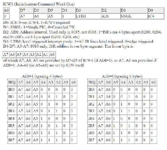
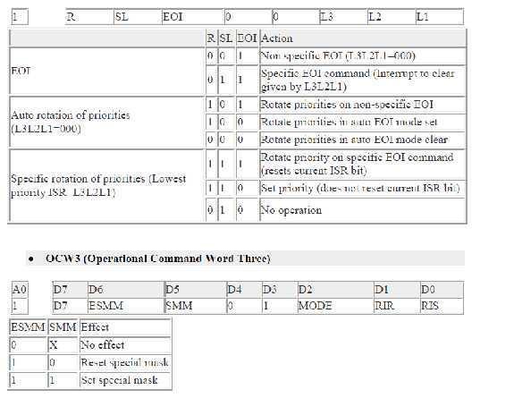
3 13. What are the features used mode 1 in 8255? Two groups group A and group B are available for strobed data transfer. 1. Each group contains one 8-bit data I/O port and one 4-bit control/data port. 2. The 8-bit data port can be either used as input or output port. The inputs and outputs both are latched. 3. Out of 8-bit port C, PC0-PC2 is used to generate control signals for port B and PC3=PC5 are used to generate control signals for port A. The lines PC6, PC7 may be used as independent data lines. 14. What are the features used mode 2 in 8255? The single 8-bit port in-group A is available. 1. The 8-bit port is bi-directional and additionally a 5-bit control port is available. 2. Three I/O lines are available at port C, viz PC2-PC0. 3. Inputs and outputs are both latched. 4. The 5-bit control port C (PC3=PC7) is used for generating/accepting handshake signals for the 8-bit data transfer on port A. 15. What are the modes of operations used in 8253? Each of the three counters of 8253 can be operated in one of the following six modes of operation. 1. Mode 0 (Interrupt on terminal count) 2. Mode 1 (Programmable monoshot) 3. Mode 2 (Rate generator) 4. Mode 3 (Square wave generator) 5. Mode 4 (Software triggered strobe) 6. Mode 5 (Hardware triggered strobe) 16. What are the different types of write operations used in 8253? There are two types of write operations in 8253 (1) Writing a control word register (2) Writing a count value into a count register The control word register accepts data from the data buffer and initializes the counters, as required. The control word register contents are used for (a) Initializing the operating modes (mode 0-mode4) (b) Selection of counters (counter 0- counter 2) (c) Choosing binary /BCD counters (d) Loading of the counter registers. The mode control register is a write only register and the CPU cannot read its contents. 17. Give the different types of command words used in 8259? The command words of 8259A are classified in two groups 1. Initialization command words (ICWs) 2. Operation command words (OCWs). 18. Give the operating modes of 8259a? (a) Fully Nested Mode (b) End of Interrupt (EOI) (c) Automatic Rotation (d) Automatic EOI Mode (e) Specific Rotation (f) Special Mask Mode (g) Edge and level Triggered Mode (h) Reading 8259 Status
4 (i) Poll command (j) Special Fully Nested Mode (k) Buffered mode (l) Cascade mode. 19. Define scan counter?[nov/dec2011] The scan counter has two modes to scan the key matrix and refresh the display. In the encoded mode, the counter provides binary count that is to be externally decoded to provide the scan lines for keyboard and display. In the decoded scan mode, the counter internally decodes the least significant 2 bits and provides a decoded 1 out of 4 scan on SL0-SL3.The keyboard and display both are in the same mode at a time. 20. What is the output modes used in 8279? 8279 provides two output modes for selecting the display options. 1. Display Scan In this mode, 8279 provides 8 or 16 character-multiplexed displays those can be organized as dual 4-bit or single 8-bit display units. 2. Display Entry 8279 allows options for data entry on the displays. The display data is entered for display from the right side or from the left side. 21. What are the modes used in keyboard modes? 1. Scanned Keyboard mode with 2 Key Lockout. 2. Scanned Keyboard with N-key Rollover. 3. Scanned Keyboard special Error Mode. 4. Sensor Matrix Mode. 22. What are the modes used in display modes? 1. Left Entry mode In the left entry mode, the data is entered from the left side of the display unit. 2. Right Entry Mode In the right entry mode, the first entry to be displayed is entered on the rightmost display. 23. What is the use of modem control unit in 8251? The modem control unit handles the modem handshake signals to coordinate the communication between the modem and the USART. 24. What is the use of 8251 chip? Intel s 8251A is a universal synchronous asynchronous receiver and transmitter compatible with Intel s Processors. This may be programmed to operate in any of the serial communication modes built into it. This chip converts the parallel data into a serial stream of bits suitable for serial transmission. It is also able to receive a serial stream of bits and converts it into parallel data bytes to be read by a microprocessor. 25. What are the different types of methods used for data transmission? The data transmission between two points involves unidirectional or bidirectional transmission of meaningful digital data through a medium. There are basically there modes of data transmission. (a) Simplex (b) Duplex (c) Half Duplex In simplex mode, data is transmitted only in one direction over a single communication channel For example, a computer (CPU) may transmit data for a CRT display unit in this mode.
5 In duplex mode, data may be transferred between two transceivers in both directions simultaneously. In half duplex mode, on the other hand, data transmission may take pace in either direction, but at a time data may be transmitted only in one direction. For example, a computer may communicate with a terminal in this mode. When the terminal sends data (i.e. terminal is sender). The message is received by the computer (i.e the computer is receiver). However, it is not possible to transmit data from the computer to terminal and from terminal to the computer simultaneously. 26. What are the various programmed data transfer methods? i) Synchronous data transfer ii) Asynchronous data transfer iii) Interrupt driven data transfer. 27. What is synchronous data transfer? It is a data method which is used when the I/O device and the microprocessor match in speed. To transfer a data to or from the device, the user program issues a suitable instruction addressing the device. The data transfer is completed at the end of the execution of this instruction. 28. What is asynchronous data transfer? It is a data transfer method which is used when the speed of an I/O device does not match with the speed of the microprocessor. Asynchronous data transfer is also called as Handshaking. 29. What are the functional types used in control words of 8251? The control words of 8251A are divided into two functional types. 1. Mode Instruction control word 2. Command Instruction control word Mode Instruction control word:- This defines the general operational characteristics of 8251A. Command Instruction control word:-the command instruction controls the actual operations of the selected format like enable transmit/receive, error reset and modem control. 30. Give the register organization of 8257? The 8257 perform the DMA operation over four independent DMA channels. Each of the four channels of 8257 has a pair of two 16-bit registers. DMA address register and terminal count register. Also, there are two common registers for all the channels; namely, mode set registers and status register. Thus there are a total of ten registers. The CPU selects one of these ten registers using address lines A0- A What is the function of DMA address register? Each DMA channel has one DMA address register. The function of this register is to store the address of the starting memory location, which will be accessed by the DMA channel. Thus the starting address of the memory block that will be accessed by the device is first loaded in the DMA address register of the channel. Naturally, the device that wants to transfer data over a DMA channel, will access the block of memory with the starting address stored in the DMA Address Register. 32. What is the use of terminal count register? Each of the four DMA channels of 8257 has one terminal count register. This 16-bit register is used for ascertaining that the data transfer through a DMA channel ceases or stops after the required number of DMA cycles.
6 33. What is the function of mode set register in 8257? The mode set register is used for programming the 8257 as per the requirements of the system. The function of the mode set register is to enable the DMA channels individually and also to set the various modes of operation. 34. List the operation modes of 8255 a) I.O Mode i. Mode 0-Simple Input/Output. ii. Mode 1-Strobed Input/Output (Handshake mode) iii. Mode 2-Strobed bidirectional mode b) Bit Set/Reset Mode. 35. What is a control word? It is a word stored in a register (control register) used to control the operation of a program digital device. 36. What is the purpose of control word written to control register in 8255?[APRIL/MAY2011] The control words written to control register specify an I/O function for each I.O port. The bit D7 of the control word determines either the I/O function of the BSR function. 37. What is the size of ports in 8255? Port-A: 8-bits Port-B: 8-bits Port-CU: 4-bits Port-CL: 4-bits. 38. What is interfacing? An interface is a shared boundary between the devices which involves sharing information. Interfacing is the process of making two different systems communicates with each other. 39. What is memory mapping?[nov/dec 2007] The assignment of memory addresses to various registers in a memory chip is called as memory mapping. 40. What is I/O mapping? [NOV/DEC 2007] The assignment of addresses to various I/O devices in the memory chip is called as I/O mapping. 41. What is an USART?[NOV/DEC 2007] USART stands for universal synchronous/asynchronous Receiver/Transmitter. It is a programmable communication interface that can communicate by using either synchronous or asynchronous serial data. 42. What is the use of 8251 chip? 8251 chip is mainly used as the asynchronous serial interface between the processor and the external equipment. 43. The 8279 is a programmable interface. Keyboard/Display List the major components of the keyboard/display interface. a. Keyboard section b. Scan section c. Display section
.")
7 d. CPU interface section. 45. What is Key bouncing? Mechanical switches are used as keys in most of the keyboards. When a key is pressed the contact bounce back and forth and settle down only after a small time delay (about 20ms). Even though a key is actuated once, it will appear to have been actuated several times. This problem is called Key Bouncing. 46. Basic concepts in memory interfacing The primary function of memory interfacing is that the microprocessor should be able to read from and write into a given register of a memory chip. To perform these operations the microprocessor should Be able to select the chip Identify the register Enable the appropriate buffer. 47. Define HRQ? The hold request output requests the access of the system bus. In non- cascaded 8257 systems, this is connected with HOLD pin of CPU. In cascade mode, this pin of a slave is connected with a DRQ input line of the master 8257, while that of the master is connected with HOLD input of the CPU. 48. What is the use of stepper motor? A stepper motor is a device used to obtain an accurate position control of rotating shafts. A stepper motor employs rotation of its shaft in terms of steps, rather than continuous rotation as in case of AC or DC motor. 49. What is TXD? TXD- Transmitter Data Output 50. What is RXD? RXD- Receive Data Input This input pin of 8251A receives a composite stream of the data to be received by 8251A. 42. How many address lines in a 4096 x 8 EPROM CHIP? 12 address lines. 43. Control signals used for DMA operation are HOLD & HLDA. 44. Differentiate between absolute and linear select decoding?
.")
8 Part B (16 Marks) 1. Memory interfacing: The memory is made up of semiconductor material used to store the programs and data. Three types of memory is, Process memory Primary or main memory Secondary memory Typical EPROM and Static RAM A typical semiconductor memory IC will have n address pins, m data pins (or output pins).having two power supply pins (one for connecting required supply voltage (V and the other for connecting ground). The control signals needed for static RAM are chip select (chip enable), read control (output enable) and write control (write enable). The control signals needed for read operation in EPROM are chip select (chip enable) and read control (output enable). Decoder It is used to select the memory chip of processor during the execution of a program. No of IC's used for decoder is, 2-4 decoder (74LS139) 3-8 decoder (74LS138) Number of Address Pins and Data Pins in Memory ICs
9 Example for Memory Interfacing Consider a system in which the full memory space 64kb is utilized for EPROM memory. Interface the EPROM with 8085 processor. The memory capacity is 64 Kbytes. i.e 2^n = 64 x 1000 bytes where n = address lines. So, n = 16. In this system the entire 16 address lines of the processor are connected to address input pins of memory IC in order to address the internal locations of memory. The chip select (CS) pin of EPROM is permanently tied to logic low (i.e., tied to ground). Since the processor is connected to EPROM, the active low RD pin is connected to active low output enable pin of EPROM. The range of address for EPROM is 0000H to FFFFH. 2. Parallel communication interfacing: Programmable peripheral interface (8255): Architecture of 8255: The parallel input-output port chip 8255 is also called as programmable peripheral input output port. The Intel s 8255 is designed for use with Intel s 8-bit, 16-bit and higher capability microprocessors. It has 24 input/output lines which may be individually programmed in two groups of twelve lines each, or three groups of eight lines. The two groups of I/O pins are named as Group A and Group B. Each of these two groups contains a subgroup of eight I/O lines called as 8-bit port and another subgroup of four lines or a 4-bit port. Thus Group A contains an 8-bit port A along with a 4-bit port. C upper.the port A lines are identified by symbols PA0-PA7 while the port C lines are identified as PC4-PC7. Similarly, GroupB contains an 8-bit port B, containing lines PB0-PB7 and a 4-bit port C with lower bits PC0 - PC3. The port C upper and port C lower can be used in combination as an 8-bit port C. Both the port C are assigned the same address. Thus one may have either three 8-bit I/O ports or two 8-bit and two 4-bit ports from All of these ports can function independently either as input or as output ports. This can be achieved by programming the bits of an internal register of 8255 called as control word register ( CWR ). This buffer receives or transmits data upon the execution of input or output instructions by the microprocessor. The control words or status information is also transferred through the buffer.

10 Block diagram of 8255: Pin diagram of 8255:
11 The signal description of 8255 are briefly presented as follows : PA7-PA0: These are eight port A lines that acts as either latched output or buffered input lines depending upon the control word loaded into the control word register. PC7-PC4 : Upper nibble of port C lines. They may act as either output latches or input buffers lines.this port also can be used for generation of handshake lines in mode 1 or mode 2. PC3-PC0 : These are the lower port C lines, other details are the same as PC7-PC4 lines. PB0-PB7 : These are the eight port B lines which are used as latched output lines or buffered input lines in the same way as port A. RD : This is the input line driven by the microprocessor and should be low to indicate read operation to WR : This is an input line driven by the microprocessor. A low on this line indicates write operation. CS : This is a chip select line. If this line goes low, it enables the 8255 to respond to RD and WR signals, otherwise RD and WR signal are neglected. A1-A0 : These are the address input lines and are driven by the microprocessor. These lines A1-A0 with RD, WR and CS from the following operations for These address lines are used for addressing any one of the four registers,i.e. three ports and a control word register as given in table below. In case of 8086 systems, if the 8255 is to be interfaced with lower order data bus, the A0 and A1 pins of 8255 are connected with A1 and A2 respectively. D0-D7 : These are the data bus lines those carry data or control word to/from the microprocessor. RESET : A logic high on this line clears the control word register of All ports are set as input ports by default after reset. 3. Modes of operation in 8255: Operational Modes of There are two operational modes of Input / Output mode 2. Bit set / reset mode. Input / Output Mode There are three types of the input/output mode. They are as follows: Mode 5. 0 In this mode, the ports can be used for simple input/output operations without handshaking. If both port A and B are initialized in mode 0, the two halves of port C can be either used together as an additional 8-bit port, or they can be used as individual 4-bit ports. Since the two halves of port C are independent, they may be used such that one-half is initialized as an input port while the other half is initialized as an output port. The input output features in mode 0 are as follows: 1. O/p are latched. 2. I/p are buffered not latched. 3. Port do not have handshake or interrupt capability.
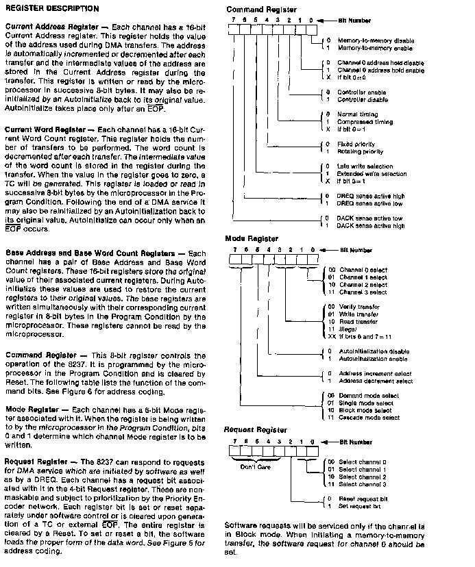
12 Mode 1 6. When we wish to use port A or port B for handshake (strobed) input or output operation, we initialize that port in mode 1 (port A and port B can be initialized to operate in different modes, ie, for eg, port A can operate in mode 0 and port B in mode 1). Some of the pins of port C function as handshake lines. For port B in this mode (irrespective of whether is acting as an input port or output port), PC0, PC1 and PC2 pins function as handshake lines. If port A is initialised as mode 1 input port, then, PC3, PC4 and PC5 function as handshake signals. Pins PC6 and PC7 are available for use as input/output lines. The mode 1 which supports handshaking has following features: 1. Two ports i.e. port A and B can be use as 8 -bit i/o port. 2. Each port uses three lines of port c as handshake signal and remaining two signals can be function as i/o port. 3. interrupt logic is supported. 4. Input and Output data are latched. Mode 2 Only group A can be initialised in this mode. Port A can be used for bidirectional handshake data transfer. This means that data can be input or output on the same eight lines (PA0 - PA7). Pins PC3 - PC7 are used as handshake lines for port A. The remaining pins of port C (PC0 - PC2) can be used as input/output lines if group B is initialised in mode 0. In this mode, the 8255 may be used to extend the system bus to a slave microprocessor or to transfer data bytes to and from a floppy disk controller. Bit Set/Reset (BSR) mode In this mode only port b can be used (as an output port). Each line of port C (PC0 - PC7) can be set/reset by suitably loading the command word register.no effect occurs in input-output mode. The individual bits of port c can be set or reset by sending the signal OUT instruction to the control register. Control Word Format Input/output mode format Control Word format in input/output mode The figure shows the control word format in the input/output mode. This mode is selected by making D7 = '1'. D0, D1, D3, D4 are for lower port C, port B, upper port C and port A respectively. When D0 or D1 or D3 or D4 are "SET", the corresponding ports act as input ports. For eg, if D0 = D4 = '1', then lower port C and port A act as input ports. If these bits are "RESET", then the corresponding ports act as output ports. For eg, if D1 = D3 = '0', then port B and upper port C act as output ports. D2 is used for mode selection for group B (Port B and Lower Port C). When D2 = '0', mode 0 is selected and when D2 = '1', mode 1 is selected. D5, D6 are used for mode selection for group A (Upper Port C and Port A). The format is as follows: D6 D5 mode x 2
 is SET, when D0 = '0', the port C bit is RESET.")
13 BSR mode format Control Word format in BSR mode The figure shows the control word format in BSR mode. This mode is selected by making D7='0'. D0 is used for bit set/reset. When D0= '1', the port C bit selected (selection of a port C bit is shown in the next point) is SET, when D0 = '0', the port C bit is RESET. D1, D2, D3 are used to select a particular port C bit whose value may be altered using D0 bit as mentioned above. The selection of the port C bits are done as follows:

14 D4, D5, D6 are not used. 4. Programmable Interrupt Controller(8259) Features 8 levels of interrupts. Can be cascaded in master-slave configuration to handle 64 levels of interrupts. Internal priority resolver. Fixed priority mode and rotating priority mode. Individually maskable interrupts. Modes and masks can be changed dynamically. Accepts IRQ, determines priority, checks whether incoming priority > current level being serviced, issues interrupt signal. In 8085 mode, provides 3 byte CALL instruction. In 8086 mode, provides 8 bit vector number. Polled and vectored mode. Starting address of ISR or vector number is programmable. No clock required. Pin diagram:
15 Pin description:
16 Block diagram:
17

18
19 5. Serial communication interface: UNIVERSAL SYNCHRONOUS ASYNCHRONOUS RECEIVER TRANSMITTER (USART) The 8251 is a USART (Universal Synchronous Asynchronous Receiver Transmitter) for serial data communication. As a peripheral device of a microcomputer system, the 8251receives parallel data from the CPU and transmits serial data after conversion. This device also receives serial data from the outside and transmits parallel data to the CPU after conversion. Block Diagram of 8251 Control Words There are two types of control word. 1. Mode instruction (setting of function) 2. Command (setting of operation)
20 1) Mode Instruction Mode instruction is used for setting the function of the Mode instruction will be in "wait for write" at either internal reset or external reset. That is, the writing of a control word after resetting will be recognized as a "mode instruction." Items set by mode instruction are as follows: Synchronous/asynchronous mode Stop bit length (asynchronous mode) Character length Parity bit Baud rate factor (asynchronous mode) Internal/external synchronization (synchronous mode) Number of synchronous characters (Synchronous mode) The bit configuration of mode instruction is shown in Figures 2 and 3. In the case of synchronous mode, it is necessary to write one-or two byte sync characters. If sync characters were written, a function will be set because the writing of sync characters constitutes part of mode instruction
21 2) Command Command is used for setting the operation of the It is possible to write a command whenever necessary after writing a mode instruction and sync characters. Items to be set by command are as follows: Transmit Enable/Disable Receive Enable/Disable DTR, RTS Output of data. Resetting of error flag. Sending to break characters Internal resetting Hunt mode (synchronous mode) CSE Department of
22

23 7. Keyboard / display controller: Programmable Keyboard/Display Interface A programmable keyboard and display interfacing chip. Scans and encodes up to a 64- key keyboard. Controls up to a 16-digit numerical display. Keyboard section has a built-in FIFO 8 character buffer. The display is controlled from an internal 16x8 RAM that stores the coded display information. Pin diagram: A0: Selects data (0) or control/status (1) for reads and writes between micro and BD: Output that blanks the displays. CLK: Used internally for timing. Max is 3 MHz. CN/ST: Control/strobe, connected to the control key on the keyboard CS: Chip select that enables programming, reading the keyboard, etc. DB7-DB0: Consists of bidirectional pins that connect to data bus on micro. IRQ: Interrupt request, becomes 1 when a key is pressed, data is available. OUT A3-A0/B3-B0: Outputs that sends data to the most significant/least significant nibble of display. RD(WR): Connects to micro's IORC or RD signal, reads data/status registers. RESET: Connects to system RESET. RL7-RL0: Return lines are inputs used to sense key depression in the keyboard matrix. Shift: Shift connects to Shift key on keyboard. SL3-SL0: Scan line outputs scan both the keyboard and displays.
24 Block diagram of 8279: Display section: The display section has eight output lines divided into two groups A0-A3 and B0-B3. The output lines can be used either as a single group of eight lines or as two groups of four lines, in conjunction with the scan lines for a multiplexed display. The output lines are connected to the anodes through driver transistor in case of common cathode 7-segment LEDs. The cathodes are connected to scan lines through driver transistors. The display can be blanked by BD (low) line. The display section consists of 16 x 8 display RAM. The CPU can read from or write into any location of the display RAM. Scan section: The scan section has a scan counter and four scan lines, SL0 to SL3. In decoded scan mode, the output of scan lines will be similar to a 2-to-4 decoder. In encoded scan mode, the output of scan lines will be binary count, and so an external decoder should be used to convert the binary count to decoded output. The scan lines are common for keyboard and display. The scan lines are used to form the rows of a matrix keyboard and also connected to digit drivers of a multiplexed display, to turn ON/OFF. CPU interface section: The CPU interface section takes care of data transfer between 8279 and the processor. This section has eight bidirectional data lines DB0 to DB7 for data transfer between
, RD (low), CS (low) and A0 are used for read/write to 8279.")

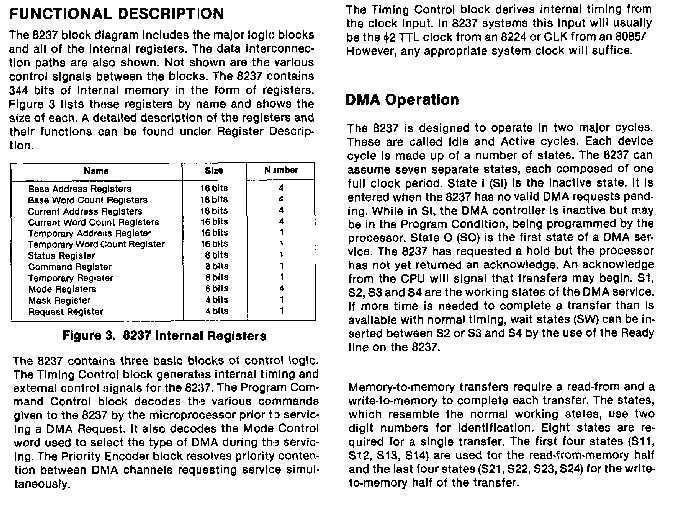
25 8279 and CPU. It requires two internal address A =0 for selecting data buffer and A = 1 for selecting control register of8279. The control signals WR (low), RD (low), CS (low) and A0 are used for read/write to It has an interrupt request line IRQ, for interrupt driven data transfer with processor. The 8279 require an internal clock frequency of 100 khz. This can be obtained by dividing the input clock by an internal prescaler. The RESET signal sets the 8279 in 16-character display with two -key lockout keyboard modes. 8. DMA controller (8237): Block diagram:

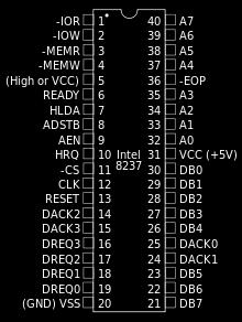
26 Pin diagram:
27

28
29
30

31 9. I / O interfacing with 8085: Interfacing I/O devices with 8085 Techniques for I/O Interfacing: Peripheral-mapped I/O 2.Memory-mapped I/O Memory-mapped I/O 8085 uses its 16-bit address bus to identify a memory location Memory address space: 0000H to FFFFH 8085 needs to identify I/O devices also I/O devices can be interfaced using addresses from memory space 8085 treats such an I/O device as a memory location This is called Memory-mapped I/O. Peripheral-mapped I/O 8085 has a separate 8-bit addressing scheme for I/O devices I/O address space: 00H to FFH This is called Peripheral-mapped I/O or I/O-mapped I/O 8085 Communication with I/O devices Involves the following three steps 1. Identify the I/O device (with address) 2. Generate Timing & Control signals 3. Data transfer takes place 8085 communicates with a I/O device only if there is a Program Instruction to do so Identify the I/O device (with address) 1. Memory-mapped I/O (16-bit address) 2. Peripheral-mapped I/O (8-bit address) Timing & Control Signals: Memory-mapped I/O Reading Input: IO/M = 0, RD = 0 Write to Output: IO/M = 0, WR = 0 Peripheral-mapped I/O Reading Input: IO/M = 1, RD = 0 Write to Output: IO/M = 1, WR = 0
32 8085 Communication with I/O devices Involves the following three steps Identify the I/O device (with address) Generate Timing & Control signals Data transfer takes place 8085 communicates with a I/O device only if there is a Program Instruction to do so Peripheral I/O Instructions IN Instruction Inputs data from input device into the accumulator It is a 2-byte instruction Format: IN 8-bit port address Example: IN 01H OUT Instruction Outputs the contents of accumulator to an output device It is a 2-byte instruction Format: OUT 8-bit port address Example: OUT 02H Memory-mapped I/O Instructions I/O devices are identified by 16-bit addresses 8085 communicates with an I/O device as if it were one of the memory locations Memory related instructions are used For e.g. LDA, STA LDA 8000H Loads A with data read from input device with 16-bit address 8000H STA 8001H Stores (Outputs) contents of A to output device with 16-bit address 8001H 11. Stepper motor: Stepper Motor: The hardware setup consists of a microprocessor motherboard and stepper motor interface board. The motherboard consists of 8085 MPU, 8KB EPROM, 8KB RAM, Keyboard and display controller 8279, 21-key Hex-keypad and six numbers of seven segment LEDs and Bus Expansion connector. The stepper motor interface consists of driver transistors for stepper motor windings and address decoding circuit. The microprocessor output the binary sequence through data bus, which are converted to current pulses by the driver transistors and used to drive stepper motor. The software for the system is developed in 8085 assembly language.
33 12. Temperature control: The temperature controller can be used to control the temperature of any plant. Typically it contains a Processor unit, Temperature input unit and Control output unit. The 8085 based motherboard forms the processing unit. The Analog-to-Digital unit together with temperature sensor forms the temperature input unit. The relay driver forms the control output unit. Electric power to the heating element (coil) is supplied through relay contacts. The switching ON/OFF of the relay controls the heat supplied to the plant.
34 Operationally, the system requires two set points-upper and lower, to be entered by the user. Whenever the temperature of the plant exceeds the upper limit or recede the lower limit relay is turned-off, so that a temperature is maintained within limits. The software for the temperature controller is developed in 8085 assembly language programs. The hardware consists of 8085 microprocessor motherboard, ADC interface board, andrelay and driver unit. The motherboard consists of 8085 MPU, 8KB EPROM, 8KB RAM keyboard and display controller 8279, programmable peripheral interface 8255, 21 key hex-keypad and six numbers of seven segment LED s. Ports Expansion connector parallel port connectors are provided for external interfacing. The temperature input board or ADC interface board consists of ADC 0809, which is an 8- bit converter with eight channels of input. It is interfaced with the motherboard through 50-pin bus expansion connector. The temperature sensor ADC590 is used to sense the temperature of the plant and its analog output is applied to the channel-0 of ADC. Relay is switched ON/OFF by driving the transistor to saturation/cut-off which is connected to port A of CS2252 MICROPROCESSORS & MICROCONTROLLERS 34
1. What is Microprocessor? Give the power supply & clock frequency of 8085?
 1. What is Microprocessor? Give the power supply & clock frequency of 8085? A microprocessor is a multipurpose, programmable logic device that reads binary instructions from a storage device called memory
Topics. Interfacing chips
 8086 Interfacing ICs 2 Topics Interfacing chips Programmable Communication Interface PCI (8251) Programmable Interval Timer (8253) Programmable Peripheral Interfacing - PPI (8255) Programmable DMA controller
8255 Programmable Peripheral Interface Architecture MCT/UNIT III/NARASIMHARAJ/LECTURE NOTES /IV MECH A
 8255 Programmable Peripheral Interface Architecture 8255 PPI Architecture The parallel input-output port chip 8255 is also called as programmable peripheral input- output port. The Intel s 8255 is designed
UNIT - II PERIPHERAL INTERFACING WITH 8085
 UNIT - II PERIPHERAL INTERFACING WITH 8085 Peripheral Interfacing is considered to be a main part of Microprocessor, as it is the only way to interact with the external world. The interfacing happens with
EC6504-MP&MC, UNIT3 Page 1
 Year/sem: 02/04 UNIT III I/O INTERFACING Academic Year: 2014-2015 (even) 1. What is interfacing? An interface is a shared boundary between the devices which involves sharing information. Interfacing is
9. PERIPHERAL CHIPS 9a
 9. PERIPHERAL CHIPS 9a 8255: Programmable Peripheral Interface. Draw the pin diagram of PPI 8255. Ans. The pin diagram of 8255 is shown in Fig. 9a. PA 3 4 PA 4 PA2 2 39 PA 5 PA 3 38 PA 6 PA 4 37 PA7 RD
Features: 3 8-bit IO ports PA, PB, PC. PA can be set for Modes 0, 1, 2. PB for 0,1 and PC for mode 0 and for BSR. Modes 1 and 2 are interrupt driven.
 Features: 3 8-bit IO ports PA, PB, PC PA can be set for Modes, 1, 2. PB for,1 and PC for mode and for BSR. Modes 1 and 2 are interrupt driven. PC has 2 4-bit parts: PC upper (PCU) and PC lower (PCL), each
This set of Microprocessor Multiple Choice Questions & Answers (MCQs) focuses on PIO 8255 (Programmable Input Output Port).
 focuses on PIO 8255 (Programmable Input Output Port).") This set of Microprocessor Multiple Choice Questions & Answers (MCQs) focuses on PIO 8255 (Programmable Input Output Port). 1. Programmable peripheral input-output port is other name for a) serial input-output
This set of Microprocessor Multiple Choice Questions & Answers (MCQs) focuses on PIO 8255 (Programmable Input Output Port). 1. Programmable peripheral input-output port is other name for a) serial input-output
EC2304-MICROPROCESSOR AND MICROCONROLLERS 2 marks questions and answers UNIT-I
 EC2304-MICROPROCESSOR AND MICROCONROLLERS 2 marks questions and answers 1. Define microprocessors? UNIT-I A semiconductor device(integrated circuit) manufactured by using the LSI technique. It includes
PIO 8255 (cont..) M Krishna kumar MAM/M3/LU9e/V1/2004 1
 M Krishna kumar MAM/M3/LU9e/V1/2004 1") PIO 8255 (cont..) The parallel input-output port chip 8255 is also called as programmable peripheral input-output port. The Intel s 8255 is designed for use with Intel s 8-bit, 16-bit and higher capability
PIO 8255 (cont..) The parallel input-output port chip 8255 is also called as programmable peripheral input-output port. The Intel s 8255 is designed for use with Intel s 8-bit, 16-bit and higher capability
UNIT V MICRO CONTROLLER PROGRAMMING & APPLICATIONS TWO MARKS. 3.Give any two differences between microprocessor and micro controller.
 UNIT V -8051 MICRO CONTROLLER PROGRAMMING & APPLICATIONS TWO MARKS 1. What is micro controller? Micro controller is a microprocessor with limited number of RAM, ROM, I/O ports and timer on a single chip
QUESTION BANK CS2252 MICROPROCESSOR AND MICROCONTROLLERS
 FATIMA MICHAEL COLLEGE OF ENGINEERING & TECHNOLOGY Senkottai Village, Madurai Sivagangai Main Road, Madurai -625 020 QUESTION BANK CS2252 MICROPROCESSOR AND MICROCONTROLLERS UNIT 1 - THE 8085 AND 8086
Unit-IV Peripheral Interfacing S.Sayeekumar, AP/RMDEEE
 Unit-IV Peripheral Interfacing S.Sayeekumar, AP/RMDEEE 8251 The 8251A is a programmable serial communication interface chip designed for synchronous and asynchronous serial data communication. It supports
Question Bank Microprocessor and Microcontroller
 QUESTION BANK - 2 PART A 1. What is cycle stealing? (K1-CO3) During any given bus cycle, one of the system components connected to the system bus is given control of the bus. This component is said to
Control Unit: The control unit provides the necessary timing and control Microprocessor resembles a CPU exactly.
 Unit I 8085 and 8086 PROCESSOR Introduction to microprocessor A microprocessor is a clock-driven semiconductor device consisting of electronic logic circuits manufactured by using either a large-scale
EC6504 MICROPROCESSOR AND MICROCONTROLLER
 UNIT I THE 8086 MICROPROCESSOR 1. What do you mean by Addressing modes? (May/June 2014) The different ways that a microprocessor can access data are referred to as addressing modes. 2. What is meant by
1. INTRODUCTION TO MICROPROCESSOR AND MICROCOMPUTER ARCHITECTURE:
 1. INTRODUCTION TO MICROPROCESSOR AND MICROCOMPUTER ARCHITECTURE: A microprocessor is a programmable electronics chip that has computing and decision making capabilities similar to central processing unit
2. List the five interrupt pins available in INTR, TRAP, RST 7.5, RST 6.5, RST 5.5.
 DHANALAKSHMI COLLEGE OF ENGINEERING DEPARTMENT OF ELECTRICAL AND ELECTRONICS ENGINEERING EE6502- MICROPROCESSORS AND MICROCONTROLLERS UNIT I: 8085 PROCESSOR PART A 1. What is the need for ALE signal in
PART B UNIT II PART A
 SRM INSTITUTE OF SCIENCE AND TECHNOLOGY (Deemed University) DEPARTMENT OF COMPUTER SCIENCE AND ENGINEERING QUESTION BANK SUB : Microprocessor/CS201 YEAR/SEM : II/III UNIT I PART - A 1. Differentiate accumulator
MCQ From PICT College of Engineering
 1. Intel s programmable device (8253) facilitates the generation of accurate time delays. a) counter b) timer c) both a & b d) none of these 2. The programmable timer device (8253) contains three independent
S.R.M. INSTITUTE OF SCIENCE & TECHNOLOGY SCHOOL OF ELECTRONICS & COMMUNICATION ENGINEERING
 S.R.M. INSTITUTE OF SCIENCE & TECHNOLOGY SCHOOL OF ELECTRONICS & COMMUNICATION ENGINEERING QUESTION BANK Subject Code : EC307 Subject Name : Microprocessor and Interfacing Year & Sem : III Year, V Sem
Pin Description, Status & Control Signals of 8085 Microprocessor
 Pin Description, Status & Control Signals of 8085 Microprocessor 1 Intel 8085 CPU Block Diagram 2 The 8085 Block Diagram Registers hold temporary data. Instruction register (IR) holds the currently executing
AE66/AC66/AT66/ AE108/AC108/AT108 MICROPROCESSORS & MICROCONTROLLERS
 Q.2 a. Draw pin diagram and signal group diagram of 8085 microprocessor. (8) b. List out the various categories of the 8085 instructions. Give examples of the instructions for each group. (8) Data transfer
Lecture Note On Microprocessor and Microcontroller Theory and Applications
 Lecture Note On Microprocessor and Microcontroller Theory and Applications MODULE: 1 1. INTRODUCTION TO MICROPROCESSOR AND MICROCOMPUTER ARCHITECTURE: A microprocessor is a programmable electronics chip
BASIC INTERFACING CONCEPTS
 Contents i SYLLABUS UNIT - I 8085 ARCHITECTURE Introduction to Microprocessors and Microcontrollers, 8085 Processor Architecture, Internal Operations, Instructions and Timings, Programming the 8085-Introduction
These three counters can be programmed for either binary or BCD count.
 S5 KTU 1 PROGRAMMABLE TIMER 8254/8253 The Intel 8253 and 8254 are Programmable Interval Timers (PTIs) designed for microprocessors to perform timing and counting functions using three 16-bit registers.
1 MALP ( ) Unit-1. (1) Draw and explain the internal architecture of 8085.
 Unit-1. (1) Draw and explain the internal architecture of 8085.") (1) Draw and explain the internal architecture of 8085. The architecture of 8085 Microprocessor is shown in figure given below. The internal architecture of 8085 includes following section ALU-Arithmetic
(1) Draw and explain the internal architecture of 8085. The architecture of 8085 Microprocessor is shown in figure given below. The internal architecture of 8085 includes following section ALU-Arithmetic
Unit DMA CONTROLLER 8257
 DMA CONTROLLER 8257 In microprocessor based system, data transfer can be controlled by either software or hardware. To transfer data microprocessor has to do the following tasks: Fetch the instruction
INTERFACING INTERFACING. Richa Upadhyay Prabhu. NMIMS s MPSTME February 25, 2016
 INTERFACING Richa Upadhyay Prabhu NMIMS s MPSTME richa.upadhyay@nmims.edu February 25, 2016 8255: Programmable Peripheral Interface or Programmable Input output Device Introduction METHODS OF DATA TRANSFER
CS2252 Microprocessor & Microcontroller TWO MARKS
 CS2252 Microprocessor & Microcontroller TWO MARKS 1. What is Microprocessor? Give the power supply & clock frequency of 8085. A microprocessor is a multipurpose, programmable logic device that reads binary
8254 is a programmable interval timer. Which is widely used in clock driven digital circuits. with out timer there will not be proper synchronization
 8254 is a programmable interval timer. Which is widely used in clock driven digital circuits. with out timer there will not be proper synchronization between two devices. So it is very useful chip. The
MICROPROCESSOR MICROPROCESSOR. From the above description, we can draw the following block diagram to represent a microprocessor based system: Output
 8085 SATISH CHANDRA What is a Microprocessor? The word comes from the combination micro and processor. Processor means a device that processes whatever. In this context, processor means a device that processes
8086 Interrupts and Interrupt Responses:
 UNIT-III PART -A INTERRUPTS AND PROGRAMMABLE INTERRUPT CONTROLLERS Contents at a glance: 8086 Interrupts and Interrupt Responses Introduction to DOS and BIOS interrupts 8259A Priority Interrupt Controller
EC1362 Microprocessors & Microcontrollers
 Part A- Two Mark Questions 1. What is Microprocessor? It is a program controlled semiconductor device (IC}, which fetches, decodes and executes instructions. 2. What are the basic units of a microprocessor?
MAHALAKSHMI ENGINEERING COLLEGE TIRUCHIRAPALLI UNIT I THE 8085 & 8086 MICROPROCESSORS. PART A (2 Marks)
") MAHALAKSHMI ENGINEERING COLLEGE TIRUCHIRAPALLI-621213. UNIT I THE 8085 & 8086 MICROPROCESSORS PART A (2 Marks) 1. Give the significance of SIM and RIM instruction available in 8085. [NOV/DEC 2006] Instruction
MAHALAKSHMI ENGINEERING COLLEGE TIRUCHIRAPALLI-621213. UNIT I THE 8085 & 8086 MICROPROCESSORS PART A (2 Marks) 1. Give the significance of SIM and RIM instruction available in 8085. [NOV/DEC 2006] Instruction
Microprocessor and Microcontroller question bank. 1 Distinguish between microprocessor and microcontroller.
 Course B.E(EEE) Batch 2015 Semester V Subject code subject Name UAEE503 Microprocessor and Microcontroller question bank UNIT-1 Architecture of a Microprocessor PART-A Marks: 2 1 Distinguish between microprocessor
SYLLABUS UNIT - I 8086/8088 ARCHITECTURE AND INSTRUCTION SET
 1 SYLLABUS UNIT - I 8086/8088 ARCHITECTURE AND INSTRUCTION SET Intel 8086/8088 Architecture Segmented Memory, Minimum and Maximum Modes of Operation, Timing Diagram, Addressing Modes, Instruction Set,
ROEVER ENGINEERING COLLEGE
 ROEVER ENGINEERING COLLEGE ELAMBALUR, PERAMBALUR- 621 212 DEPARTMENT OF INFORMATION TECHNOLOGY MICROPROCESSOR & MICROCONTROLLER 2 marks questions andanswers Unit I 1. Define microprocessor? A microprocessor
CS 1304-MICROPROCESSORS
 CS 1304-MICROPROCESSORS 1. What is Microprocessor? Give the power supply & clock frequency of 8085 A microprocessor is a multipurpose, programmable logic device that reads binary instructions from a storage
Interfacing Fundamentals
 CHAPTER Interfacing Fundamentals 3.1 Introduction There is no doubt that the microcomputer revolution will continue into the future and many will be required to specify and integrate microprocessors into
MICROPROCESSORS & INTERFACING (A1423) C.Lokanath Reddy Assistant Professor.
 C.Lokanath Reddy Assistant Professor.") MICROPROCESSORS & INTERFACING (A1423) C.Lokanath Reddy Assistant Professor clreddy@vardhaman.org Department of Electronics and Communication Engineering VARDHAMAN COLLEGE OF ENGINEERING (AUTONOMOUS) Shamshabad,
MICROPROCESSORS & INTERFACING (A1423) C.Lokanath Reddy Assistant Professor clreddy@vardhaman.org Department of Electronics and Communication Engineering VARDHAMAN COLLEGE OF ENGINEERING (AUTONOMOUS) Shamshabad,
Computer Organization and Microprocessors SYLLABUS CHAPTER - 1 : BASIC STRUCTURE OF COMPUTERS CHAPTER - 3 : THE MEMORY SYSTEM
 i SYLLABUS UNIT - 1 CHAPTER - 1 : BASIC STRUCTURE OF COMPUTERS Computer Types, Functional Units, Basic Operational Concepts, Bus Structures, Software, Performance, Multiprocessors and Multicomputers, Historical
History and Basic Processor Architecture
 History and Basic Processor Architecture History of Computers Module 1 Section 1 What Is a Computer? An electronic machine, operating under the control of instructions stored in its own memory, that can
 VALLIAMMAI ENGINEERING COLLEGE S.R.M. NAGAR, KATTANKULATHUR-603203. DEPARTMENT OF ELECTRICAL AND ELECTRONICS ENGINEERING VII-EEE EE6502- MICROPROCESSORS AND MICROCONTROLLERS QUESTION BANK UNIT I 1. What
Microprocessor Architecture
 Microprocessor - 8085 Architecture 8085 is pronounced as "eighty-eighty-five" microprocessor. It is an 8-bit microprocessor designed by Intel in 1977 using NMOS technology. It has the following configuration
MICROPROCESSOR AND MICROCONTROLLER BASED SYSTEMS
 MICROPROCESSOR AND MICROCONTROLLER BASED SYSTEMS UNIT I INTRODUCTION TO 8085 8085 Microprocessor - Architecture and its operation, Concept of instruction execution and timing diagrams, fundamentals of
CHAPTER 5 : Introduction to Intel 8085 Microprocessor Hardware BENG 2223 MICROPROCESSOR TECHNOLOGY
 CHAPTER 5 : Introduction to Intel 8085 Hardware BENG 2223 MICROPROCESSOR TECHNOLOGY The 8085A(commonly known as the 8085) : Was first introduced in March 1976 is an 8-bit microprocessor with 16-bit address
CREATED BY M BILAL & Arslan Ahmad Shaad Visit:
 CREATED BY M BILAL & Arslan Ahmad Shaad Visit: www.techo786.wordpress.com Q1: Define microprocessor? Short Questions Chapter No 01 Fundamental Concepts Microprocessor is a program-controlled and semiconductor
INSTITUTE OF ENGINEERING AND MANAGEMENT, KOLKATA Microprocessor
 INSTITUTE OF ENGINEERING AND MANAGEMENT, KOLKATA Microprocessor Subject Name: Microprocessor and Microcontroller Year: 3 rd Year Subject Code: CS502 Semester: 5 th Module Day Assignment 1 Microprocessor
1. (a) Draw the internal architecture of 8085? Explain each block. (b) What are the special functions of GPRs in 8086? And explain them?
 Draw the internal architecture of 8085? Explain each block. (b) What are the special functions of GPRs in 8086? And explain them?") Code No: R05220504 Set No. 1 1. (a) Draw the internal architecture of 8085? Explain each block. (b) What are the special functions of GPRs in 8086? And explain them? 2. Explain clearly with examples the
Code No: R05220504 Set No. 1 1. (a) Draw the internal architecture of 8085? Explain each block. (b) What are the special functions of GPRs in 8086? And explain them? 2. Explain clearly with examples the
Architecture of 8085 microprocessor
 Architecture of 8085 microprocessor 8085 consists of various units and each unit performs its own functions. The various units of a microprocessor are listed below Accumulator Arithmetic and logic Unit
It is a program controlled semiconductor device (IC}, which fetches, decode and executes instructions.
 1.What is Microprocessor? It is a program controlled semiconductor device (IC}, which fetches, decode and executes instructions. 2. What are the basic units of a microprocessor? The basic units or blocks
QUESTION BANK. EE 6502 / Microprocessor and Microcontroller. Unit I Processor. PART-A (2-Marks)
") QUESTION BANK EE 6502 / Microprocessor and Microcontroller Unit I- 8085 Processor PART-A (2-Marks) YEAR/SEM : III/V 1. What is meant by Level triggered interrupt? Which are the interrupts in 8085 level
QUESTION BANK EE 6502 / Microprocessor and Microcontroller Unit I- 8085 Processor PART-A (2-Marks) YEAR/SEM : III/V 1. What is meant by Level triggered interrupt? Which are the interrupts in 8085 level
Chapter 1: Basics of Microprocessor [08 M]
![Chapter 1: Basics of Microprocessor [08 M]](/thumbs/77/75860546.jpg "Chapter 1: Basics of Microprocessor [08 M]") Microprocessor: Chapter 1: Basics of Microprocessor [08 M] It is a semiconductor device consisting of electronic logic circuits manufactured by using either a Large scale (LSI) or Very Large Scale (VLSI)
Microprocessor: Chapter 1: Basics of Microprocessor [08 M] It is a semiconductor device consisting of electronic logic circuits manufactured by using either a Large scale (LSI) or Very Large Scale (VLSI)
4. (a) With a neat sketch explain 8237 DMA controller and its operation? (b) With the help of basic cell explain SRAM and DRAM?
 With a neat sketch explain 8237 DMA controller and its operation? (b) With the help of basic cell explain SRAM and DRAM?") Code No: R05220504 Set No. 1 II B.Tech II Semester Regular Examinations, Apr/May 2008 MICROPROCESSORS AND INTERFACING ( Common to Computer Science & Engineering, Information Technology and Computer Science
Code No: R05220504 Set No. 1 II B.Tech II Semester Regular Examinations, Apr/May 2008 MICROPROCESSORS AND INTERFACING ( Common to Computer Science & Engineering, Information Technology and Computer Science
Chapter 8 Summary: The 8086 Microprocessor and its Memory and Input/Output Interface
 Chapter 8 Summary: The 8086 Microprocessor and its Memory and Input/Output Interface Figure 1-5 Intel Corporation s 8086 Microprocessor. The 8086, announced in 1978, was the first 16-bit microprocessor
Microprocessors and Interfacng. Question bank
 Microprocessors & Interfacing 8086 ARCHITECTURE: UNIT-I Functional Diagram, Register Organization, Addressing modes, Instructions, Functional schematic, Minimum and Maximum mode operations of 8086, 8086
1. Internal Architecture of 8085 Microprocessor
 1. Internal Architecture of 8085 Microprocessor Control Unit Generates signals within up to carry out the instruction, which has been decoded. In reality causes certain connections between blocks of the
INSTITUTE OF AERONAUTICAL ENGINEERING (Autonomous) Dundigal, Hyderabad
 Dundigal, Hyderabad") INSTITUTE OF AERONAUTICAL ENGINEERING (Autonomous) Dundigal, Hyderabad - 500 043 COMPUTER SCIENCE AND ENGINEERING TUTORIAL QUESTION BANK Name : MICROPROCESSORS AND INTERFACING Code : AEC021 Class : B.
INSTITUTE OF AERONAUTICAL ENGINEERING (Autonomous) Dundigal, Hyderabad - 500 043 COMPUTER SCIENCE AND ENGINEERING TUTORIAL QUESTION BANK Name : MICROPROCESSORS AND INTERFACING Code : AEC021 Class : B.
Basics of Microprocessor
 Unit 1 Basics of Microprocessor 1. Microprocessor Microprocessor is a multipurpose programmable integrated device that has computing and decision making capability. This semiconductor IC is manufactured
In this tutorial, we will discuss the architecture, pin diagram and other key concepts of microprocessors.
 About the Tutorial A microprocessor is a controlling unit of a micro-computer, fabricated on a small chip capable of performing Arithmetic Logical Unit (ALU) operations and communicating with the other
EC 6504 Microprocessor and Microcontroller. Unit II System Bus Structure
 EC 6504 Microprocessor and Microcontroller Unit II 8086 System Bus Structure Syllabus: 8086 Signals Basic Configurations System bus timing System Design using 8086 IO Programming Introduction to multiprogramming
UNIT-IV. The semiconductor memories are organized as two-dimensional arrays of memory locations.
 UNIT-IV MEMORY INTERFACING WITH 8086: The semi conductor memories are of two types: Static RAM Dynamic RAM The semiconductor memories are organized as two-dimensional arrays of memory locations. For Ex:
BHARATHIDASAN ENGINEERING COLLEGE. III Year / V Semester / EEE MICROPROCESSORS AND MICROCONTROLLERS (R-2013)
") BHARATHIDASAN ENGINEERING COLLEGE III Year / V Semester / EEE MICROPROCESSORS AND MICROCONTROLLERS (R-2013) FREQUENTLY ASKED QUESTIONS IN UNIVERSITY EXAMINATION PART A UNIT 1-8085 PROCESSOR 1. Draw the
BHARATHIDASAN ENGINEERING COLLEGE III Year / V Semester / EEE MICROPROCESSORS AND MICROCONTROLLERS (R-2013) FREQUENTLY ASKED QUESTIONS IN UNIVERSITY EXAMINATION PART A UNIT 1-8085 PROCESSOR 1. Draw the
FIFTH SEMESTER B.TECH DEGREE EXAMINATION MODEL TEST QUESTION PAPER, NOVEMBER CS 305: Microprocessor and Microcontrollers PART A
 Reg No Name FIFTH SEMESTER B.TECH DEGREE EXAMINATION MODEL TEST QUESTION PAPER, NOVEMBER 2017 CS 305: Microprocessor and Microcontrollers Max. Marks: 100 Duration: 3 Hours PART A Answer all questions.
Lecture-51 INTEL 8259A Programmable Interrupt Controller
 Lecture-51 INTEL 8259A Programmable Interrupt Controller The 8259A is a programmable interrupt controller designed to work with Intel microprocessor 8080 A, 8085, 8086, 8088. The 8259 A interrupt controller
CHAPTER: 3 PROGRAMMABLE PERIPHERAL INTERFACE & ELECTROMECHANICAL DEVICES INTERFACING
 CHAPTER: 3 1 PROGRAMMABLE PERIPHERAL INTERFACE & ELECTROMECHANICAL DEVICES INTERFACING Introduction to 8255 PPI 2 The Intel 8255A is a high-performance, general purpose programmable I/O device is designed
TOPIC 6 LATCH. FIGURE 1 INTERFACING OF ROM/EPROM TO µc 8051.
 TOPIC 6 MEMORY AND I/O INTERFACING MEMORY INTERFACING i. External ROM (program memory) Interfacing P1 P0 D 0-D 7 P3 EA clock LATCH A 0 ROM/ A 7 EPROM A 8 Address lines A 15 PSEN OE FIGURE 1 INTERFACING
1. Define Peripherals. Explain I/O Bus and Interface Modules. Peripherals: Input-output device attached to the computer are also called peripherals.
 1. Define Peripherals. Explain I/O Bus and Interface Modules. Peripherals: Input-output device attached to the computer are also called peripherals. A typical communication link between the processor and
Module 3. Embedded Systems I/O. Version 2 EE IIT, Kharagpur 1
 Module 3 Embedded Systems I/O Version 2 EE IIT, Kharagpur 1 Lesson 15 Interrupts Version 2 EE IIT, Kharagpur 2 Instructional Objectives After going through this lesson the student would learn Interrupts
Code No: RR Set No. 1
 Code No: RR310501 Set No. 1 1. (a) If an absolute address of the type 6A3D9H is given, express it in the form of CS : IP and explain what are the advantages of the memory segmentation. Discuss about the
SANKALCHAND PATEL COLLEGE OF ENGINEERING, VISNAGAR. ELECTRONICS & COMMUNICATION DEPARTMENT Question Bank- 1
 SANKALCHAND PATEL COLLEGE OF ENGINEERING, VISNAGAR ELECTRONICS & COMMUNICATION DEPARTMENT Question Bank- 1 Subject: Microcontroller and Interfacing (151001) Class: B.E.Sem V (EC-I & II) Q-1 Explain RISC
To Interface The 8085 Microprocessor
 To Interface The 8085 Microprocessor A microprocessor has to be interfaced with various peripherals to perform various functions. Let's discuss about the Interfacing techniques in detail. Introduction
Lecture-50 Intel 8255A: Programming and Operating Modes
 Lecture-50 Intel 8255A: Programming and Operating Modes Operation Description: There are three basic modes of operation that can be selected by the system software. Mode 0: Basic Input/output Mode 1: Strobes
INTRO TO I/O INTERFACE
 Basic I/O Interface Introduction This chapter outlines some of the basic methods of communications, both serial and parallel, between humans or machines and the microprocessor. We first introduce the basic
EC 6504 MICROPROCESSOR AND MICROCONTROLLER
 DEPARTMENTOFELECTRONICS&COMMUNICATIONENGINEERING EC 6504 MICROPROCESSOR AND MICROCONTROLLER UNIT I THE 8086 MICROPROCESSOR PARTA 1. What is microprocessor? What is the difference between a MP and CPU?
Interrupts. by Rahul Patel, Assistant Professor, EC Dept., Sankalchand Patel College of Engg.,Visnagar
 Chapter 12 Interrupts by Rahul Patel, Assistant Professor, EC Dept., Sankalchand Patel College of Engg.,Visnagar Microprocessor & Interfacing (140701) Rahul Patel 1 Points to be Discussed 8085 Interrupts
PART B (5 x 16 =80) ADDRESS BUS The 8085 has eight signal lines, A15 A8 : Unidirectional, known as high order address.
 ADDRESS BUS The 8085 has eight signal lines, A15 A8 : Unidirectional, known as high order address.") PART B (5 x 16 =80) 1. Explain with a help of neat diagram of Pin out details of 8085 microprocessor. Intel 8085 consists of 40 pins and signal can be classified as follow: Address Bus. Data Bus. Control
PART B (5 x 16 =80) 1. Explain with a help of neat diagram of Pin out details of 8085 microprocessor. Intel 8085 consists of 40 pins and signal can be classified as follow: Address Bus. Data Bus. Control
Registers Format. 4.1 I/O Port Address
 4 Registers Format The detailed descriptions of the register format and structure of the ACL- 8112 are specified in this chapter. This information is quite useful for the programmer who wish to handle
VALLIAMMAI ENGINEERING COLLEGE
 VALLIAMMAI ENGINEERING COLLEGE SRM Nagar, Kattankulathur 603 203 DEPARTMENT OF ELECTRICAL AND ELECTRONICS ENGINEERING QUESTION BANK V SEMESTER EE6502- MICROPROCESSORS AND MICROCONTROLLERS Regulation 2013
Chapter 4 : Microprocessor System
 Chapter-4 Microprocessor System A microcomputer consists of a set of components or modules of three basic types CPU memory and I/O units which communicate with each other. PIN Configuration of 8085 Fig
INPUT-OUTPUT ORGANIZATION
 INPUT-OUTPUT ORGANIZATION Peripheral Devices: The Input / output organization of computer depends upon the size of computer and the peripherals connected to it. The I/O Subsystem of the computer, provides
3. (a) Explain the steps involved in the Interfacing of an I/O device (b) Explain various methods of interfacing of I/O devices.
 Explain the steps involved in the Interfacing of an I/O device (b) Explain various methods of interfacing of I/O devices.") Code No: R05320202 Set No. 1 1. (a) Discuss the minimum mode memory control signals of 8086? (b) Explain the write cycle operation of the microprocessor with a neat timing diagram in maximum mode. [8+8]
Code No: R05320202 Set No. 1 1. (a) Discuss the minimum mode memory control signals of 8086? (b) Explain the write cycle operation of the microprocessor with a neat timing diagram in maximum mode. [8+8]
The Purpose of Interrupt
 Interrupts 3 Introduction In this chapter, the coverage of basic I/O and programmable peripheral interfaces is expanded by examining a technique called interrupt-processed I/O. An interrupt is a hardware-initiated
7/19/2013. Introduction. Chapter Objectives Upon completion of this chapter, you will be able to: Chapter Objectives 12 1 BASIC INTERRUPT PROCESSING
 Chapter 12: Interrupts Introduction In this chapter, the coverage of basic I/O and programmable peripheral interfaces is expanded by examining a technique called interrupt-processed I/O. An interrupt is
Computer Organization (Keyboard & Display Control, and Printers)
") Computer Organization (Keyboard & Display Control, and Printers) KR Chowdhary Professor & Head Email: kr.chowdhary@gmail.com Website:krchowdhary.com Department of Computer Science and Engineering MBM Engineering
Computer Organization (Keyboard & Display Control, and Printers) KR Chowdhary Professor & Head Email: kr.chowdhary@gmail.com Website:krchowdhary.com Department of Computer Science and Engineering MBM Engineering
Chapter 12: Interrupts
 Chapter 12: Interrupts Introduction In this chapter, the coverage of basic I/O and programmable peripheral interfaces is expanded by examining a technique called interrupt-processed I/O. An interrupt is
Micro Processor & Micro Controllers
 Micro Processor & Micro Controllers 1. What is microprocessor? It is a program controlled semi conductor device (IC), which fetches, decodes and execute instructions. 2. What are the basic units of microprocessor?
Chapter 13 Direct Memory Access and DMA-Controlled I/O
 Chapter 13 Direct Memory Access and DMA-Controlled I/O The DMA I/O technique provides direct access to the memory while the microprocessor is temporarily disabled This allows data to be transferred between
8051 Microcontroller
 8051 Microcontroller 1 Salient Features (1). 8 bit microcontroller originally developed by Intel in 1980. (2). High-performance CMOS Technology. (3). Contains Total 40 pins. (4). Address bus is of 16 bit
DEPARTMENT OF ECE QUESTION BANK SUBJECT: MICROPROCESSOR AND MICROCONTROLLER UNIT-1 PART-A (2 MARKS)
") DEPARTMENT OF ECE QUESTION BANK SUBJECT: MICROPROCESSOR AND MICROCONTROLLER CODE: EC6504 UNIT-1 1. How many memory locations are available in 8086 microprocessor? 2. What are the flags available in 8086
DEPARTMENT OF ECE QUESTION BANK SUBJECT: MICROPROCESSOR AND MICROCONTROLLER CODE: EC6504 UNIT-1 1. How many memory locations are available in 8086 microprocessor? 2. What are the flags available in 8086
UNIT 3 THE 8051-REAL WORLD INTERFACING
 UNIT 3 THE 8051-REAL WORLD INTERFACING 8031/51 INTERFACING TO EXTERNAL MEMORY The number of bits that a semiconductor memory chip can store is called chip capacity It can be in units of Kbits (kilobits),
PROGRAMMABLE PERIPHERAL INTERFACE (PPI) -8255
 -8255") PROGRAMMABLE PERIPHERAL INTERFACE (PPI) -8255 8255 is a general purpose programmable device used for data transfer between processor and I/O devices. It has 3 programmable I/O ports (PA,PB &PC) and port
PROGRAMMABLE PERIPHERAL INTERFACE (PPI) -8255 8255 is a general purpose programmable device used for data transfer between processor and I/O devices. It has 3 programmable I/O ports (PA,PB &PC) and port
Address connections Data connections Selection connections
 Interface (cont..) We have four common types of memory: Read only memory ( ROM ) Flash memory ( EEPROM ) Static Random access memory ( SARAM ) Dynamic Random access memory ( DRAM ). Pin connections common
1. What is microprocessor? It is a program controlled semi conductor device (IC), which fetches, decodes and execute instructions.
, which fetches, decodes and execute instructions.") Downloaded from www.books4career.blogspot.com 1. What is microprocessor? It is a program controlled semi conductor device (IC), which fetches, decodes and execute instructions. 2. What are the basic units
Downloaded from www.books4career.blogspot.com 1. What is microprocessor? It is a program controlled semi conductor device (IC), which fetches, decodes and execute instructions. 2. What are the basic units
DHANALAKSHMI COLLEGE OF ENGINEERING DEPARTMENT OF ELECTRICAL AND ELECTRONICS ENGINEERING YEAR : III SEM : VI
 DHANALAKSHMI COLLEGE OF ENGINEERING DEPARTMENT OF ELECTRICAL AND ELECTRONICS ENGINEERING YEAR : III SEM : VI EE2354- MICROPROCESSORS AND MICROCONTROLLER UNIT I 8085 and 8086 PROCESSOR PART A 1. Define
UNIT II OVERVIEW MICROPROCESSORS AND MICROCONTROLLERS MATERIAL. Introduction to 8086 microprocessors. Architecture of 8086 processors
 OVERVIEW UNIT II Introduction to 8086 microprocessors Architecture of 8086 processors Register Organization of 8086 Memory Segmentation of 8086 Pin Diagram of 8086 Timing Diagrams for 8086 Interrupts of
I/O Design. Input / Output Instructions. Engineering 4862 Microprocessors. Lecture 23. Cheng Li
 Engineering 4862 Microprocessors Lecture 23 Cheng Li EN-4012 licheng@engr.mun.ca I/O Design When designing an I/O port, ensure that the port is only active when selected by the microprocessor Use latches
UNIT.4. Syllabus I/O INTERFACING 8085
 UNIT.4 I/O INTERFACING 8085 Syllabus Memory Interfacing and I/O interfacing Parallel communication interface Serial communication interface Timer Keyboard /display controller Interrupt controller DMA controller
Instructions Involve a Segment Register (SR-field)
") BYTE 1 = 11000111 2 = C7 16 BYTE 2 = (MOD)000(R/M) = 100000112 = 83 16 BYTE 3 = 34 16 and BYTE 4 = 12 16 BYTE 5 = CD 16 and BYTE 6 = AB 16 The machine code for the instruction is: MOV [BP+DI+1234H], 0ABCDH
BYTE 1 = 11000111 2 = C7 16 BYTE 2 = (MOD)000(R/M) = 100000112 = 83 16 BYTE 3 = 34 16 and BYTE 4 = 12 16 BYTE 5 = CD 16 and BYTE 6 = AB 16 The machine code for the instruction is: MOV [BP+DI+1234H], 0ABCDH