Quilt Packaging For Power Electronics
|
|
|
- Ashlynn Weaver
- 6 years ago
- Views:
Transcription
1 Quilt Packaging For Power Electronics 21 March 2013 Jason M. Kulick President, Co-Founder Indiana Integrated Circuits, LLC
2 Overview Introduction Quilt Packaging (QP) technology Concept Examples Advantages QP progress in power 2

3 Indiana Integrated Circuits, LLC (IIC) Formed to commercialize QP Located in South Bend, IN Licensing/prototyping biz model Successive funding rounds through Series A (8/2012) Steady growth in QP & R&D Contract R&D Experience: E-Beam Lithography Specialty Plating DRIE & ICP etching IC & MEMs prototyping Magnetics/nanomagnetic fabrication & testing 3

4 Quilt Packaging (QP) Technology Edge-connections joined to create multi-chip quilt, developed at Notre Dame Monolithic assemblies from same or disparate materials & process technologies Extremely low impedances Enables optimization for cost and functionality Industry-standard tools and fabrication processes CHIP 1 CHIP 2 4

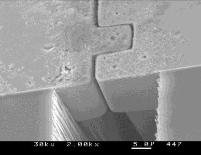
5 QP-Interconnect Structures Edge connection structures called nodules Solid metal, typically um wide, ~ um thick Customizable shapes-including interlocking-enables sub-micron chip alignment 5
6 QP Customizable I/O 6
 of")

7 Sub-Micron Chip Alignment = 30 micron Interior (left) of four-chip quilt (above) QP enable extremely accurate alignment 7
")
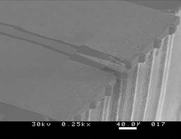
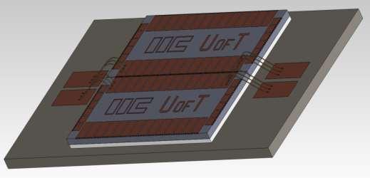
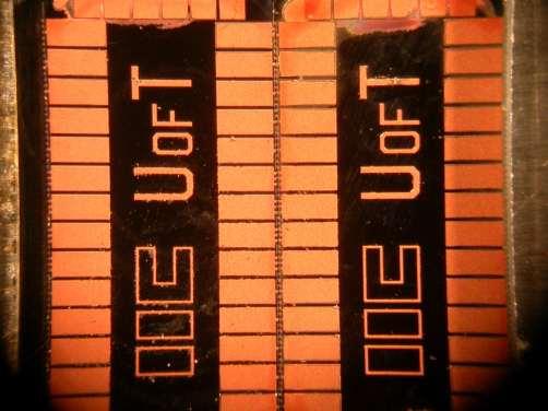
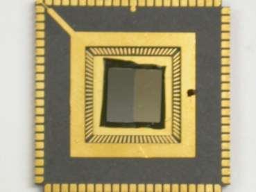
8 Si QP 2x2 Array (1 in^2 chips) 8

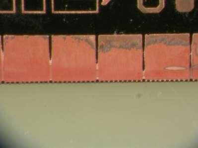
9 ~15 um gap post-solder 9

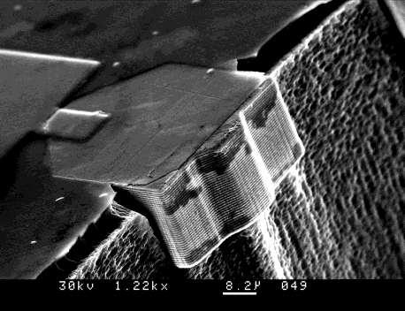
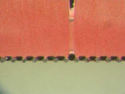
10 Inner seam of 4-chip Si test quilt 10

11 4-chip quilt mechanically strong 11

12 GaAs QP Chipset 12


13 GaAs Measurement Data Sample Raw S-parameters De-embedded S-parameters *Less than 3 db insertion loss at 220 GHz
14 QP Microwave Performance Less than 0.1 db insertion loss from 50 MHz past 100 GHz, with no resonances. Recent unpublished results under 0.9 db at 180 GHz 14

 = 12.")
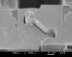
15 QP Eye diagrams Measurement of 12 Gb/s eye pattern (Anritsu MP1763B) Horiz. 100 mv/div Vert. 20 ps/div Data stream: pseudorandom bit sequence Nearly ideal interconnect performance; indistinguishable from PG. Error-free operation SNR (Q) = 12.9 for pattern generator alone, 12.4 after chip-to-chip interconnect Raw pattern generator 50 µm GSG eye 15
16 QP Time-Domain Performance Single-ended GSG CPW configuration Picosecond Pulse Labs 4022 TDR pulse enhancement module: < 9 ps risetime Total delay including probe pads, launcher: 7 ps (820 μm length) Delay due to QP nodules: 2.7 ps 100 µm nodule compared with pads/launcher, GSG 16


17 3D-QP and Interposers QP can enable multiple 3D configurations 3D-QP retains many advantages of 2D-QP Quilting interposers can decrease formfactor Systems benefit from QP without having to redesign chips 17


18 3D Si QP Test Articles 18
19 Advantages of Quilt Packaging Optimized integration of disparate materials and process technologies (Si, GaN, GaAs, AlN, more) Chip partitioning for optimal yield/functionality Increased cross-sectional area vs. WBs, bumps Better thermal management & failure modes compared to WB Reduced design time due to applicability of current 2-D tools, design re-use IP flexibility, security 19
20 Original intent-test using wirebonds 20
21 Early test articles--couldn t wirebond, had to probe directly 21

22 Joule heating simulation through nodules interconnect (setup) DC Source Electrode Copper Sn Solder Silicon Ground Electrode 22

23 Joule heating simulation through quilted interconnect (no showstoppers) 23
24 Temperature (C) Simulations don t include heatsink, nodule size 30 um X 20 um Temperature Across Quilted Nodule (30um x 25 um cross area) w/ Metal 1 From Applied Current Current (A) 24
, nodule size 30 um X 20")
25 Si QP Max current probe test (before), nodule size 30 um X 20 um 25

26 Si QP Max current test--probes fail before nodules (~2.25A) 26


27 Potential Uses of QP In Power Electronics Load Low-cost Power-optimized 12V BCD Passive Die L & C Driver + HV Power Stage + Protection High-speed Mixed-Signal I/O SoC Load ~ 1V Digital optimized CMOS 27 High-current, low ESR, ESL Power Connection


28 Potential Uses of QP In Power Electronics Load Low-cost CMOS or BCD Passive Die L & C High-speed Mixed-Signal I/O Optimized High- Speed Driver + Protection HV GaN/GAs Power Stage SoC Load ~ 1V Digital optimized CMOS 28 High-current, low ESR, ESL Power Connection
29 Potential Uses of QP In Power Electronics Load BCD or GaN/GAs with On-chip drivers Driver + HV Power Stage + Passives on Silicon High-speed Mixed-Signal I/O SoC Load ~1V Digital optimized CMOS 29 High-current, low ESR, ESL Power Connection
30 Future Work Thermal cycle/shock testing of preliminary quilts (ongoing) Completion of DC-DC converter demonstration (3-chip quilt w/qp Si interposer---ongoing) GaN QP (just starting) Chip architectures & partitioning for power Other?---Specific partner applications, etc. 30
31 Thank You! For More Information Contact: Jason Kulick (574) And/or visit: 31
32 QP Fabrication Process Flow Overview Very similar to via-middle TSV process Utilizes industry-standard tools & processes At least 2 additional mask steps Nodule definition Separation Most unique feature is dry etch step for singulation After assembly, handle as if normal chip 32
33 QP Fabrication-Nodule Definition 33

34 QP Fabrication- Nodule Metallization 34

35 QP Fabrication-Die Singulation 35
Quilt Packaging Microchip Interconnect Technology
 Quilt Packaging Microchip Interconnect Technology 18 November 2012 Jason M. Kulick President, Co-Founder Indiana Integrated Circuits, LLC Overview Introduction to IIC Quilt Packaging (QP) Concept Electrical
Beyond Chip Stacking---Quilt Packaging Enabled 3D Systems
 Beyond Chip Stacking---Quilt Packaging Enabled 3D Systems Jason Kulick, President & Co-Founder jason.kulick@indianaic.com 574-217-4612 (South Bend, IN) May 3, 2016 2016 New England IMAPS Symposium Presentation
Multi-Die Packaging How Ready Are We?
 Multi-Die Packaging How Ready Are We? Rich Rice ASE Group April 23 rd, 2015 Agenda ASE Brief Integration Drivers Multi-Chip Packaging 2.5D / 3D / SiP / SiM Design / Co-Design Challenges: an OSAT Perspective
Photonics Integration in Si P Platform May 27 th Fiber to the Chip
 Photonics Integration in Si P Platform May 27 th 2014 Fiber to the Chip Overview Introduction & Goal of Silicon Photonics Silicon Photonics Technology Wafer Level Optical Test Integration with Electronics
Stacked Silicon Interconnect Technology (SSIT)
") Stacked Silicon Interconnect Technology (SSIT) Suresh Ramalingam Xilinx Inc. MEPTEC, January 12, 2011 Agenda Background and Motivation Stacked Silicon Interconnect Technology Summary Background and Motivation
Stacked Silicon Interconnect Technology (SSIT) Suresh Ramalingam Xilinx Inc. MEPTEC, January 12, 2011 Agenda Background and Motivation Stacked Silicon Interconnect Technology Summary Background and Motivation
Passive MMIC 60GHz Equalizer
 Page 1 The is a passive MMIC equalizer. It is a positive gain slope equalizer designed to pass DC to 60GHz. Equalization can be applied to reduce low pass filtering effects in both RF/microwave and high
Embedded UTCP interposers for miniature smart sensors
 Embedded UTCP interposers for miniature smart sensors T. Sterken 1,2, M. Op de Beeck 2, Tom Torfs 2, F. Vermeiren 1,2, C. Van Hoof 2, J. Vanfleteren 1,2 1 CMST (affiliated with Ugent and IMEC), Technologiepark
Application Note. Pyramid Probe Cards
 Application Note Pyramid Probe Cards Innovating Test Technologies Pyramid Probe Technology Benefits Design for Test Internal pads, bumps, and arrays High signal integrity Rf and DC on same probe card Small
IMEC CORE CMOS P. MARCHAL
 APPLICATIONS & 3D TECHNOLOGY IMEC CORE CMOS P. MARCHAL OUTLINE What is important to spec 3D technology How to set specs for the different applications - Mobile consumer - Memory - High performance Conclusions
Burn-in & Test Socket Workshop
 Burn-in & Test Socket Workshop IEEE March 4-7, 2001 Hilton Mesa Pavilion Hotel Mesa, Arizona IEEE COMPUTER SOCIETY Sponsored By The IEEE Computer Society Test Technology Technical Council COPYRIGHT NOTICE
Xilinx SSI Technology Concept to Silicon Development Overview
 Xilinx SSI Technology Concept to Silicon Development Overview Shankar Lakka Aug 27 th, 2012 Agenda Economic Drivers and Technical Challenges Xilinx SSI Technology, Power, Performance SSI Development Overview
MARKET PERSPECTIVE: SEMICONDUCTOR TREND OF 2.5D/3D IC WITH OPTICAL INTERFACES PHILIPPE ABSIL, IMEC
 MARKET PERSPECTIVE: SEMICONDUCTOR TREND OF 2.5D/3D IC WITH OPTICAL INTERFACES PHILIPPE ABSIL, IMEC OUTLINE Market Trends & Technology Needs Silicon Photonics Technology Remaining Key Challenges Conclusion
MicraGEM-Si A flexible process platform for complex MEMS devices
 MicraGEM-Si A flexible process platform for complex MEMS devices By Dean Spicer, Jared Crawford, Collin Twanow, and Nick Wakefield Introduction MicraGEM-Si is a process platform for MEMS prototyping and
EECS 598: Integrating Emerging Technologies with Computer Architecture. Lecture 10: Three-Dimensional (3D) Integration
 Integration") 1 EECS 598: Integrating Emerging Technologies with Computer Architecture Lecture 10: Three-Dimensional (3D) Integration Instructor: Ron Dreslinski Winter 2016 University of Michigan 1 1 1 Announcements
1 EECS 598: Integrating Emerging Technologies with Computer Architecture Lecture 10: Three-Dimensional (3D) Integration Instructor: Ron Dreslinski Winter 2016 University of Michigan 1 1 1 Announcements
3D SYSTEM INTEGRATION TECHNOLOGY CHOICES AND CHALLENGE ERIC BEYNE, ANTONIO LA MANNA
 3D SYSTEM INTEGRATION TECHNOLOGY CHOICES AND CHALLENGE ERIC BEYNE, ANTONIO LA MANNA OUTLINE 3D Application Drivers and Roadmap 3D Stacked-IC Technology 3D System-on-Chip: Fine grain partitioning Conclusion
A Fine Pitch MEMS Probe Card with Built in Active Device for 3D IC Test
 3000.0 2500.0 2000.0 1500.0 1000.0 500.0 0.00-500.0-1000.0-1500.0 OSCILLOSCOPE Design file: MSFT DIFF CLOCK WITH TERMINATORREV2.FFS Designer: Microsoft HyperLynx V8.0 Comment: 650MHz at clk input, J10,
Challenges of Integration of Complex FHE Systems. Nancy Stoffel GE Global Research
 Challenges of Integration of Complex FHE Systems Nancy Stoffel GE Global Research Products drive requirements to sub-systems, components and electronics GE PRODUCTS CTQs: SWaP, $$, operating environment,
Applications, Processing and Integration Options for High Dielectric Constant Multi-Layer Thin-Film Barium Strontium Titanate (BST) Capacitors
 Capacitors") Applications, Processing and Integration Options for High Dielectric Constant Multi-Layer Thin-Film Barium Strontium Titanate (BST) Capacitors Agenda Introduction What is BST? Unique Characteristics of
Applications, Processing and Integration Options for High Dielectric Constant Multi-Layer Thin-Film Barium Strontium Titanate (BST) Capacitors Agenda Introduction What is BST? Unique Characteristics of
3D Integration & Packaging Challenges with through-silicon-vias (TSV)
") NSF Workshop 2/02/2012 3D Integration & Packaging Challenges with through-silicon-vias (TSV) Dr John U. Knickerbocker IBM - T.J. Watson Research, New York, USA Substrate IBM Research Acknowledgements IBM
NSF Workshop 2/02/2012 3D Integration & Packaging Challenges with through-silicon-vias (TSV) Dr John U. Knickerbocker IBM - T.J. Watson Research, New York, USA Substrate IBM Research Acknowledgements IBM
From 3D Toolbox to 3D Integration: Examples of Successful 3D Applicative Demonstrators N.Sillon. CEA. All rights reserved
 From 3D Toolbox to 3D Integration: Examples of Successful 3D Applicative Demonstrators N.Sillon Agenda Introduction 2,5D: Silicon Interposer 3DIC: Wide I/O Memory-On-Logic 3D Packaging: X-Ray sensor Conclusion
Comparison of Singulation Techniques
 Comparison of Singulation Techniques Electronic Packaging Society, Silicon Valley Chapter Sept. 28, 2017 ANNETTE TENG Sept 28, 2017 1 Definition of Singulation 9/28/2017 Annetteteng@promex-ind.com 2 www.cpmt.org/scv
Physical Design Implementation for 3D IC Methodology and Tools. Dave Noice Vassilios Gerousis
 I NVENTIVE Physical Design Implementation for 3D IC Methodology and Tools Dave Noice Vassilios Gerousis Outline 3D IC Physical components Modeling 3D IC Stack Configuration Physical Design With TSV Summary
Opportunities & Challenges: 28nm & 2.5/3-D IC Design and Manufacturing
 Opportunities & Challenges: 28nm & 2.5/3-D IC Design and Manufacturing Vincent Tong Senior Vice President & Asia Pacific Executive Leader Copyright 2011 Xilinx Agenda Xilinx Business Drivers All in at
Power Matters. TM. Why Embedded Die? Piers Tremlett Microsemi 22/9/ Microsemi Corporation. Company Proprietary 1
 Power Matters. TM Why Embedded Die? Piers Tremlett Microsemi 22/9/16 1 Introduction This presentation: Outlines our journey to make miniaturised SiP modules Compares : Embedded Die Technology (EDT) With
High performance HBM Known Good Stack Testing
 High performance HBM Known Good Stack Testing FormFactor Teradyne Overview High Bandwidth Memory (HBM) Market and Technology Probing challenges Probe solution Power distribution challenges PDN design Simulation
Bringing 3D Integration to Packaging Mainstream
 Bringing 3D Integration to Packaging Mainstream Enabling a Microelectronic World MEPTEC Nov 2012 Choon Lee Technology HQ, Amkor Highlighted TSV in Packaging TSMC reveals plan for 3DIC design based on silicon
MPS4101-6LP Datasheet 50 MHz 25 GHz RoHS-Compliant Control Device QFN SPST PIN
 MPS4101-6LP Datasheet 50 MHz 25 GHz RoHS-Compliant Control Device QFN SPST PIN Microsemi Corporate Headquarters One Enterprise, Aliso Viejo, CA 92656 USA Within the USA: +1 (800) 713-4113 Outside the USA:
3D technology for Advanced Medical Devices Applications
 3D technology for Advanced Medical Devices Applications By, Dr Pascal Couderc,Jerome Noiray, Dr Christian Val, Dr Nadia Boulay IMAPS MEDICAL WORKSHOP DECEMBER 4 & 5,2012 P.COUDERC 3D technology for Advanced
Comparison & highlight on the last 3D TSV technologies trends Romain Fraux
 Comparison & highlight on the last 3D TSV technologies trends Romain Fraux Advanced Packaging & MEMS Project Manager European 3D Summit 18 20 January, 2016 Outline About System Plus Consulting 2015 3D
MMA043AA Datasheet 0.5 GHz 12 GHz GaAs phemt MMIC Wideband Low-Noise Amplifier
 MMA043AA Datasheet 0.5 GHz 12 GHz GaAs phemt MMIC Wideband Low-Noise Amplifier Microsemi Corporate Headquarters One Enterprise, Aliso Viejo, CA 92656 USA Within the USA: +1 (800) 713-4113 Outside the USA:
GLAST Silicon Microstrip Tracker Status
 R.P. Johnson Santa Cruz Institute for Particle Physics University of California at Santa Cruz Mechanical Design Detector Procurement Work list for the Prototype Tracker Construction. ASIC Development Hybrids
3D TECHNOLOGIES: SOME PERSPECTIVES FOR MEMORY INTERCONNECT AND CONTROLLER
 3D TECHNOLOGIES: SOME PERSPECTIVES FOR MEMORY INTERCONNECT AND CONTROLLER CODES+ISSS: Special session on memory controllers Taipei, October 10 th 2011 Denis Dutoit, Fabien Clermidy, Pascal Vivet {denis.dutoit@cea.fr}
3D systems-on-chip. A clever partitioning of circuits to improve area, cost, power and performance. The 3D technology landscape
 Edition April 2017 Semiconductor technology & processing 3D systems-on-chip A clever partitioning of circuits to improve area, cost, power and performance. In recent years, the technology of 3D integration
Verification of Singulated HBM2 stacks with Die Level Handler. Dave Armstrong Toshiyuki Kiyokawa Quay Nhin
 Verification of Singulated HBM2 stacks with Die Level Handler Dave Armstrong Toshiyuki Kiyokawa Quay Nhin Abstract Background only will delete on final material High-Bandwidth-Memory continues to evolve
MMA044AA Datasheet 6 GHz 18 GHz GaAs phemt MMIC Wideband Low-Noise Amplifier
 MMA044AA Datasheet 6 GHz 18 GHz GaAs phemt MMIC Wideband Low-Noise Amplifier Microsemi Corporate Headquarters One Enterprise, Aliso Viejo, CA 92656 USA Within the USA: +1 (800) 713-4113 Outside the USA:
Advances in Measurement Based Transient Simulation
 Time Domain Simulation in ADS, Slide - 1 Advances in Measurement Based Transient Simulation Presented by GigaTest Labs Gary Otonari and Orlando Bell March, 2008 1 Time Domain Simulation in ADS, Slide -
Development of a Design & Manufacturing Environment for Reliable and Cost- Effective PCB Embedding Technology
 Development of a Design & Manufacturing Environment for Reliable and Cost- Effective PCB Embedding Technology Outline Introduction CAD design tools for embedded components Thermo mechanical design rules
Area Array Probe Card Interposer. Raphael Robertazzi IBM Research 6/4/01. 6/4/01 IBM RESEARCH Page [1]
![Area Array Probe Card Interposer. Raphael Robertazzi IBM Research 6/4/01. 6/4/01 IBM RESEARCH Page [1]](/thumbs/78/78371092.jpg "Area Array Probe Card Interposer. Raphael Robertazzi IBM Research 6/4/01. 6/4/01 IBM RESEARCH Page [1]") Area Array Probe Card Interposer Raphael Robertazzi IBM Research 6/4/01 6/4/01 IBM RESEARCH Page [1] Motivation: Outline Probe Cards for Testing Complex ICs in the Developmental Stage. Hand Wired Space
Area Array Probe Card Interposer Raphael Robertazzi IBM Research 6/4/01 6/4/01 IBM RESEARCH Page [1] Motivation: Outline Probe Cards for Testing Complex ICs in the Developmental Stage. Hand Wired Space
Advanced Heterogeneous Solutions for System Integration
 Advanced Heterogeneous Solutions for System Integration Kees Joosse Director Sales, Israel TSMC High-Growth Applications Drive Product and Technology Smartphone Cloud Data Center IoT CAGR 12 17 20% 24%
RELIABILITY REPORT FOR. MAX485ExxA PLASTIC ENCAPSULATED DEVICES. November 19, 2002 MAXIM INTEGRATED PRODUCTS 120 SAN GABRIEL DR. SUNNYVALE, CA 94086
 MAX485ExxA Rev. A RELIABILITY REPORT FOR MAX485ExxA PLASTIC ENCAPSULATED DEVICES November 19, 2002 MAXIM INTEGRATED PRODUCTS 120 SAN GABRIEL DR. SUNNYVALE, CA 94086 Written by Reviewed by Jim Pedicord
Scanning Acoustic Microscopy For Metrology of 3D Interconnect Bonded Wafers
 Scanning Acoustic Microscopy For Metrology of 3D Interconnect Bonded Wafers Jim McKeon, Ph.D. - Sonix, Director of Technology Sriram Gopalan, Ph.D. - Sonix, Technology Engineer 8700 Morrissette Drive 8700
PLANAR LIGHTWAVE CIRCUITS FOR USE IN ADVANCED OPTICAL INSTRUMENTATION
 PLANAR LIGHTWAVE CIRCUITS FOR USE IN ADVANCED OPTICAL INSTRUMENTATION AN ENABLENCE ARTICLE WRITTEN BY DR. MATT PEARSON, VP TECHNOLOGY & ASHOK BALAKRISHNAN, DIRECTOR OF PRODUCT DEVELOPMENT PUBLISHED IN
Test and Measurement Challenges for 3D IC Development. R. Robertazzi IBM Research
 Test and Measurement Challenges for 3D IC Development R. Robertazzi IBM Research PFA Bill Price. Pete Sorce. John Ott. David Abraham. Pavan Samudrala Digital Test Kevin Stawaisz. TEL P12 Prober Glen Lansman,
Katana RFx: A New Technology for Testing High Speed RF Applications Within TI
 Katana RFx: A New Technology for Testing High Speed RF Applications Within TI Compan Logo Probe Test Solutions Manager Overview Introduction Objectives Procedures Results Summary Follow-On Work 2 Introduction
MLVS 0402 Series Engineering Specification
 MLVS 0402 Series 1. Scope This specification is applicable to Chip Metal Oxide Varistor in multilayer technology.the customer designed part number drawing take precedence over this specification. For RoHS
Abbas El Gamal. Joint work with: Mingjie Lin, Yi-Chang Lu, Simon Wong Work partially supported by DARPA 3D-IC program. Stanford University
 Abbas El Gamal Joint work with: Mingjie Lin, Yi-Chang Lu, Simon Wong Work partially supported by DARPA 3D-IC program Stanford University Chip stacking Vertical interconnect density < 20/mm Wafer Stacking
SMAFTI Package Technology Features Wide-Band and Large-Capacity Memory
 SMAFTI Package Technology Features Wide-Band and Large-Capacity Memory KURITA Yoichiro, SOEJIMA Koji, KAWANO Masaya Abstract and NEC Corporation have jointly developed an ultra-compact system-in-package
Mm-wave integrated waveguide components in silicon technology
 Mm-wave integrated waveguide components in silicon technology G. Gentile, M. Spirito, L.C.N. de Vreede, et al. Electronics Research Laboratory (ELCA), Dimes, Delft University of Technology, The Netherlands
RELIABILITY REPORT FOR MAX2055EUP PLASTIC ENCAPSULATED DEVICES. April 2, 2004 MAXIM INTEGRATED PRODUCTS 120 SAN GABRIEL DR. SUNNYVALE, CA 94086
 MAX2055EUP Rev. A RELIABILITY REPORT FOR MAX2055EUP PLASTIC ENCAPSULATED DEVICES April 2, 2004 MAXIM INTEGRATED PRODUCTS 120 SAN GABRIEL DR. SUNNYVALE, CA 94086 Written by Reviewed by Jim Pedicord Quality
Skill Development Centre by AN ISO CERTIFIED COMPANY
 Skill Development Centre by AN ISO CERTIFIED COMPANY Industrial Automation Training Embedded/ VLSI system design Electrical control panel Design Product Development Fiber optics Technician Electrician
Monolithic 3D Integration using Standard Fab & Standard Transistors. Zvi Or-Bach CEO MonolithIC 3D Inc.
 Monolithic 3D Integration using Standard Fab & Standard Transistors Zvi Or-Bach CEO MonolithIC 3D Inc. 3D Integration Through Silicon Via ( TSV ), Monolithic Increase integration Reduce interconnect total
RELIABILITY REPORT FOR PLASTIC ENCAPSULATED DEVICES MAXIM INTEGRATED PRODUCTS 120 SAN GABRIEL DR. SUNNYVALE, CA 94086
 MAX726xCK Rev. A RELIABILITY REPORT FOR MAX726xCK PLASTIC ENCAPSULATED DEVICES June 20, 2003 MAXIM INTEGRATED PRODUCTS 120 SAN GABRIEL DR. SUNNYVALE, CA 94086 Written by Reviewed by Jim Pedicord Quality
Mixed-Signal. From ICs to Systems. Mixed-Signal solutions from Aeroflex Colorado Springs. Standard products. Custom ASICs. Mixed-Signal modules
 A passion for performance. Mixed-Signal solutions from Aeroflex Colorado Springs Standard products Custom ASICs Mixed-Signal modules Circuit card assemblies Mixed-Signal From ICs to Systems RadHard ASICs
WHICH SIDE ARE YOU ON? DOUBLE SIDED PROBING
 WHICH SIDE ARE YOU ON? DOUBLE SIDED PROBING Traditionally, devices with active regions on both sides of a wafer were limited to discrete devices. With advances in materials, functionality and packaging,
Wafer Probe card solutions
 Wafer Probe card solutions Innovative Solutions to Test Chips in the Semiconductor Industry Our long term experience in the electronic industry and our strong developing and process teams are inspired
DFT-3D: What it means to Design For 3DIC Test? Sanjiv Taneja Vice President, R&D Silicon Realization Group
 I N V E N T I V E DFT-3D: What it means to Design For 3DIC Test? Sanjiv Taneja Vice President, R&D Silicon Realization Group Moore s Law & More : Tall And Thin More than Moore: Diversification Moore s
MAXIM INTEGRATED PRODUCTS
 MAX3089ExxD Rev. A RELIABILITY REPORT FOR MAX3089ExxD PLASTIC ENCAPSULATED DEVICES June 20, 2003 MAXIM INTEGRATED PRODUCTS 120 SAN GABRIEL DR. SUNNYVALE, CA 94086 Written by Reviewed by Jim Pedicord Quality
Advancing high performance heterogeneous integration through die stacking
 Advancing high performance heterogeneous integration through die stacking Suresh Ramalingam Senior Director, Advanced Packaging European 3D TSV Summit Jan 22 23, 2013 The First Wave of 3D ICs Perfecting
Getting Started. 1.3 X-MWsystem Vocabulary. X-MWprobe X-MWanchor X-MWjumper. X-MWblock RF. X-MWblock Bias and Control. X-MWprotoplate X-MWwall X-MWlid
 1. X-Microwave System (X-MWsystem) 1.1 Overview RF and Microwave design and product development is an incredibly interesting and challenging field. The Craft is truly an art and it takes years to learn
Packaging Technology for Image-Processing LSI
 Packaging Technology for Image-Processing LSI Yoshiyuki Yoneda Kouichi Nakamura The main function of a semiconductor package is to reliably transmit electric signals from minute electrode pads formed on
There is a paradigm shift in semiconductor industry towards 2.5D and 3D integration of heterogeneous parts to build complex systems.
 Direct Connection and Testing of TSV and Microbump Devices using NanoPierce Contactor for 3D-IC Integration There is a paradigm shift in semiconductor industry towards 2.5D and 3D integration of heterogeneous
MAXIM INTEGRATED PRODUCTS
 MAX3088xxA Rev. A RELIABILITY REPORT FOR MAX3088xxA PLASTIC ENCAPSULATED DEVICES February 26, 2003 MAXIM INTEGRATED PRODUCTS 120 SAN GABRIEL DR. SUNNYVALE, CA 94086 Written by Reviewed by Jim Pedicord
3D-IC is Now Real: Wide-IO is Driving 3D-IC TSV. Samta Bansal and Marc Greenberg, Cadence EDPS Monterey, CA April 5-6, 2012
 3D-IC is Now Real: Wide-IO is Driving 3D-IC TSV Samta Bansal and Marc Greenberg, Cadence EDPS Monterey, CA April 5-6, 2012 What the fuss is all about * Source : ECN Magazine March 2011 * Source : EDN Magazine
TSV Test. Marc Loranger Director of Test Technologies Nov 11 th 2009, Seoul Korea
 TSV Test Marc Loranger Director of Test Technologies Nov 11 th 2009, Seoul Korea # Agenda TSV Test Issues Reliability and Burn-in High Frequency Test at Probe (HFTAP) TSV Probing Issues DFT Opportunities
3D & Advanced Packaging
 Tuesday, October 03, 2017 Company Overview March 12, 2015 3D & ADVANCED PACKAGING IS NOW WITHIN REACH WHAT IS NEXT LEVEL INTEGRATION? Next Level Integration blends high density packaging with advanced
Non-contact Test at Advanced Process Nodes
 Chris Sellathamby, J. Hintzke, B. Moore, S. Slupsky Scanimetrics Inc. Non-contact Test at Advanced Process Nodes June 8-11, 8 2008 San Diego, CA USA Overview Advanced CMOS nodes are a challenge for wafer
MAXIM INTEGRATED PRODUCTS
 MAX6628MKA Rev. A RELIABILITY REPORT FOR MAX6628MKA PLASTIC ENCAPSULATED DEVICES September 30, 2003 MAXIM INTEGRATED PRODUCTS 120 SAN GABRIEL DR. SUNNYVALE, CA 94086 Written by Reviewed by Jim Pedicord
Gigascale Integration Design Challenges & Opportunities. Shekhar Borkar Circuit Research, Intel Labs October 24, 2004
 Gigascale Integration Design Challenges & Opportunities Shekhar Borkar Circuit Research, Intel Labs October 24, 2004 Outline CMOS technology challenges Technology, circuit and μarchitecture solutions Integration
MAXIM INTEGRATED PRODUCTS
 RELIABILITY REPORT FOR MAX11060GUU+ PLASTIC ENCAPSULATED DEVICES May 18, 2011 MAXIM INTEGRATED PRODUCTS 120 SAN GABRIEL DR. SUNNYVALE, CA 94086 Approved by Sokhom Chum Quality Assurance Reliability Engineer
ARCHIVE 2008 COPYRIGHT NOTICE
 Keynote Speaker ARCHIVE 2008 Packaging & Assembly in Pursuit of Moore s Law and Beyond Karl Johnson Ph.D. Vice President and Senior Fellow Advanced Packaging Systems Integration Laboratory Freescale Semiconductor
TQPED MMIC Design Training
 TQPED MMIC Design Training Outline Installation and Use of the Library AWR AWR Design Kit (PDK Process Design Kit) ICED Layout Kit Create a new document using the Library Environment Setup Hotkeys Background
3D Power Electronics Packaging and Additive Manufacturing
 3D Power Electronics Packaging and Additive Manufacturing Presented by Dr. Doug Hopkins NCSU DCHopkins@NCSU.edu www..org 2015 Douglas C Hopkins Packaging v. Manufacturing PACKAGING: a Design Process MANUFACTURING:
MLVG0402 Series Engineering Specification
 RoHS Pb MLVG0402 Series Engineering 1. Scope (1) Lead free type (2) SMD type zinc oxide based ceramic chip (3) Insulator over coat keeps excellent low and stable leakage current (4) Plating termination
Interconnect Challenges in a Many Core Compute Environment. Jerry Bautista, PhD Gen Mgr, New Business Initiatives Intel, Tech and Manuf Grp
 Interconnect Challenges in a Many Core Compute Environment Jerry Bautista, PhD Gen Mgr, New Business Initiatives Intel, Tech and Manuf Grp Agenda Microprocessor general trends Implications Tradeoffs Summary
THERMAL EXPLORATION AND SIGN-OFF ANALYSIS FOR ADVANCED 3D INTEGRATION
 THERMAL EXPLORATION AND SIGN-OFF ANALYSIS FOR ADVANCED 3D INTEGRATION Cristiano Santos 1, Pascal Vivet 1, Lee Wang 2, Michael White 2, Alexandre Arriordaz 3 DAC Designer Track 2017 Pascal Vivet Jun/2017
MAXIM INTEGRATED PRODUCTS
 MAX1619MEE Rev. A RELIABILITY REPORT FOR MAX1619MEE PLASTIC ENCAPSULATED DEVICES October 17, 2003 MAXIM INTEGRATED PRODUCTS 120 SAN GABRIEL DR. SUNNYVALE, CA 94086 Written by Reviewed by Jim Pedicord Quality
MAXIM INTEGRATED PRODUCTS
 MAX2720EUP Rev. A RELIABILITY REPORT FOR MAX2720EUP PLASTIC ENCAPSULATED DEVICES March 25, 2004 MAXIM INTEGRATED PRODUCTS 120 SAN GABRIEL DR. SUNNYVALE, CA 94086 Written by Reviewed by Jim Pedicord Quality
Thermo Mechanical Modeling of TSVs
 Thermo Mechanical Modeling of TSVs Jared Harvest Vamsi Krishna ih Yaddanapudi di 1 Overview Introduction to Through Silicon Vias (TSVs) Advantages of TSVs over wire bonding in packages Role of TSVs in
MAXIM INTEGRATED PRODUCTS
 MAX3378EEUD Rev. A RELIABILITY REPORT FOR MAX3378EEUD PLASTIC ENCAPSULATED DEVICES March 6, 2003 MAXIM INTEGRATED PRODUCTS 120 SAN GABRIEL DR. SUNNYVALE, CA 94086 Written by Reviewed by Jim Pedicord Quality
Technology and Manufacturing
 Technology and Manufacturing Executive Vice President Field Trip 2006 - London, May 23rd Field Trip 2006 - London, May 23rd Technology Technology Development Centers and Main Programs CMOS Logic Platform
Chapter 2 Three-Dimensional Integration: A More Than Moore Technology
 Chapter 2 Three-Dimensional Integration: A More Than Moore Technology Abstract Three-dimensional integrated circuits (3D-ICs), which contain multiple layers of active devices, have the potential to dramatically
All Programmable: from Silicon to System
 All Programmable: from Silicon to System Ivo Bolsens, Senior Vice President & CTO Page 1 Moore s Law: The Technology Pipeline Page 2 Industry Debates Variability Page 3 Industry Debates on Cost Page 4
The Foundry-Packaging Partnership. Enabling Future Performance. Jon A. Casey. IBM Systems and Technology Group
 The Foundry-Packaging Partnership Enabling Future Performance Jon A. Casey IBM Fellow IBM Systems and Technology Group 5/30/2013 2012 IBM Corporation Data growth will drive the new IT model Dimensions
LTCC (Low Temperature Co-fired Ceramic)
") LTCC (Low Temperature Co-fired Ceramic) Design Guide Line. 381, Wonchun-Dong, Paldal-Ku, Suwon City, Kyung Ki-Do, Republic of Korea Tel : 82-31-217-2500 (Ext. 470) Fax : 82-31-217-7316 Homepage : http://www.pilkorcnd.co.kr
LTCC (Low Temperature Co-fired Ceramic) Design Guide Line. 381, Wonchun-Dong, Paldal-Ku, Suwon City, Kyung Ki-Do, Republic of Korea Tel : 82-31-217-2500 (Ext. 470) Fax : 82-31-217-7316 Homepage : http://www.pilkorcnd.co.kr
Advanced CSP & Turnkey Solutions. Fumio Ohyama Tera Probe, Inc.
 Advanced CSP & Turnkey Solutions Fumio Ohyama Tera Probe, Inc. Tera Probe - Corporate Overview 1. Company : Tera Probe, Inc. 2. Founded : August, 2005 3. Capital : Approx. USD118.2 million (as of March
Rethinking the Hierarchy of Electronic Interconnections. Joseph Fjelstad Verdant Electronics
 Rethinking the Hierarchy of Electronic Interconnections Joseph Fjelstad Verdant Electronics The Industry s Terminology Challenge» The electronics industry continues to explore and develop new methods to
Next-Generation Electronic Packaging: Trend & Materials Challenges. Lai Group R&D ASE
 Next-Generation Electronic Packaging: Trend & Materials Challenges Yi-Shao Lai Group R&D ASE Jun 26, 2010 Evolution & Growth of Electronics 2 Evolution of Electronic Products Audion Tube (1906) Transistor
Il pensiero parallelo: Una storia di innovazione aziendale
 Il pensiero parallelo: Una storia di innovazione aziendale Maria Teresa Gatti Scienzazienda Trento, 8 Maggio 2006 Overview ST is one of the largest Worldwide Semiconductors provider, with products ranging
ARCHIVE Françoise von Trapp Editorial Director 3D InCites ABSTRACT
 2010 Invited Speaker ARCHIVE 2010 RISING TO THE 3D TSV TEST CHALLENGE: WILL YOU BE READY? by Françoise von Trapp Editorial Director 3D InCites 3D ABSTRACT integration is not a novel concept. Veterans in
Packaging and Integration Technologies for Silicon Photonics. Dr. Peter O Brien, Tyndall National Institute, Ireland.
 Packaging and Integration Technologies for Silicon Photonics Dr. Peter O Brien, Tyndall National Institute, Ireland. Opportunities for Silicon Photonics Stress Sensors Active Optical Cable 300 mm Silicon
MMS006AA Datasheet DC 20 GHz GaAs MMIC SP2T Non-Reflective Switch
 MMS006AA Datasheet DC 20 GHz GaAs MMIC SP2T Non-Reflective Switch Microsemi Corporate Headquarters One Enterprise, Aliso Viejo, CA 92656 USA Within the USA: +1 (800) 713-4113 Outside the USA: +1 (949)
Introduction 1. GENERAL TRENDS. 1. The technology scale down DEEP SUBMICRON CMOS DESIGN
 1 Introduction The evolution of integrated circuit (IC) fabrication techniques is a unique fact in the history of modern industry. The improvements in terms of speed, density and cost have kept constant
WLSI Extends Si Processing and Supports Moore s Law. Douglas Yu TSMC R&D,
 WLSI Extends Si Processing and Supports Moore s Law Douglas Yu TSMC R&D, chyu@tsmc.com SiP Summit, Semicon Taiwan, Taipei, Taiwan, Sep. 9 th, 2016 Introduction Moore s Law Challenges Heterogeneous Integration
Wafer Probe card solutions
 Wafer Probe card solutions Innovative Solutions to Test Chips in the Semiconductor Industry Our long term experience in the electronic industry and our strong developing and process teams are inspired
AIM Photonics: Manufacturing Challenges for Photonic Integrated Circuits
 AIM Photonics: Manufacturing Challenges for Photonic Integrated Circuits November 16, 2017 Michael Liehr Industry Driving Force EXA FLOP SCALE SYSTEM Blades SiPh Interconnect Network Memory Stack HP HyperX
D5.2: Packaging and fiber-pigtailing of the 2 nd generation 2x2 optical interconnect router
 ICT - Information and Communication Technologies Merging Plasmonics and Silicon Photonics Technology towards Tb/s routing in optical interconnects Collaborative Project Grant Agreement Number 249135 D5.2:
Micron Level Placement Accuracy for Wafer Scale Packaging of P-Side Down Lasers in Optoelectronic Products
 Micron Level Placement Accuracy for Wafer Scale Packaging of P-Side Down Lasers in Optoelectronic Products Daniel D. Evans, Jr. and Zeger Bok Palomar Technologies, Inc. 2728 Loker Avenue West Carlsbad,
MASW Dual / Tri / Quaand GSM Applications Electrical Specifications: T A = 25 C, V C = 0V/2.5V, Z 0 = 50 Ω 4 Parameter Test Conditions Units Min
 MASW000105 Dual / Tri / Quaand GSM Applications Features Dual / tri / quadband GSM / GPRS / EDGE 2.5V Operation Harmonics: 70 c @ +34.5 m & 1 GHz Insertion Loss: 0.5 @ 1 GHz T X R X Isolation: 41 @ 2 GHz
RELIABILITY REPORT FOR. MAX202ExxE PLASTIC ENCAPSULATED DEVICES. February 22, 2002 MAXIM INTEGRATED PRODUCTS 120 SAN GABRIEL DR. SUNNYVALE, CA 94086
 MAX202ExxE Rev. A RELIABILITY REPORT FOR MAX202ExxE PLASTIC ENCAPSULATED DEVICES February 22, 2002 MAXIM INTEGRATED PRODUCTS 120 SAN GABRIEL DR. SUNNYVALE, CA 94086 Written by Reviewed by Jim Pedicord