Expert Layout Editor. Technical Description
|
|
|
- Cordelia Harmon
- 6 years ago
- Views:
Transcription

1 Expert Layout Editor Technical Description
2 Agenda Expert Layout Editor Overview General Layout Editing Features Technology File Setup Multi-user Project Library Setup Advanced Programmable Features Schematic Netlist Driven Layout Parameterized Cell (Pcell) Development Real -Time DRC Design for Manufacturing - Cross Section Viewer - 2 -
3 Expert Layout Editor Productive layout environment for analog, RF, microwave, and digital layouts Flexible tuning to different IC technologies: CMOS, Bipolar, BiCMOS, SiGe, GaAs, InP and other unique processes Extremely fast loading, viewing and editing operation for multi-million transistor designs regardless available memory Integrated verification tools (DRC/ERC/LVS) for interactive or batch operation Parameterized cells (Pcells) using the powerful Lisa scripting language Same intuitive interface across Solaris, Linux, and Windows platforms - 3 -

4 Expert Inputs and Outputs Accepts GDSII, LEF/DEF, CIF, Applicon and OASIS - 4 -
 -")
5 Multi-Window Hierarchical Editing: Three Level View of Chip Hierarchy Level 1 Level 2 Design Bar Project Hierarchy Tree Layer Bar Cell Map Level 6 Hierarchy Level (6 of 9) - 5 -
 - 6")
6 Hierarchical Editing: Top Level with Routing Hierarchy Level (4 of 13) - 6 -
 - 7")
7 Hierarchical Floorplan View Hierarchy Level (4 of 13) - 7 -
 - 8")
8 Hierarchical Editing 6th Level with Routing Hierarchy Level (6 of 13) - 8 -
9 Easy to Adopt and Use Customizable hotkeys, macros, and toolbars may be set to emulate the look and feel of Virtuoso environment for layout designers Process Design Kits (PDKs) from foundries enable quick start-up of new design environments Informative, easily accessible online help for all menus and icons Linux and Windows availability enables wide deployment on economy workstations Simple installation process does not require consultants to set up environment Cross-platform floating license system with support for Virtual Network Connection (VNC) for distribute offices Drives wide selection of printers and plotters (HP, Gerber, Versatech) with multi-page tiling based on paper size - 9 -
10 High-End Layout Editing Capabilities Library management and multi-user environment Facilitated technology migration Electrical hierarchical node probing Netlist-driven layout with parameterized cells (Pcells) Numerous productivity enhancers (gravity, reference points, pre-selection, layer plans, etc.) Intelligent geometry database, offering fast processing speed and low memory requirements Arbitrary geometric shapes for device creation and DRC checks

11 All-Angle Features All angle geometries Rounded corners Text tags Rulers Derived layers Functions Useful for RF & MEMS
12 Powerful Functions For Customization and Porting Create parameterized cells (Pcells) with the Lisa scripting and graphical support Powerful C++ API can access all editing functions Auto scaling and resize feature minimizes process migration efforts Powerful hierarchical search Productivity for Power Users

13 Hierarchical Search with Edit in Place Found Object Properties Search Window Edit in Place Search Criteria
14 Interoperable with Popular Design Flows Directly imports Calibre, Dracula, and Diva DRC/ERC/LVS rule decks Reads Calibre and Dracula error reports for Result Viewing Environment (RVE) Technology file import from Virtuoso for layers, colors, stipples Customizable hotkeys, macros, and toolbars for familiar look and feel Imports legacy designs with GDSII, Applicon and CIF data


15 Calibre Error Database and Expert Error Review

16 Easy Technology File Setup with Virtuoso Import Main Layer Setup Window with GDS Layers Setup Menu Stipple Selector Layer Setup Edit Stipple Bitmap Choose Setup of Colors, Stipples, View Style Select Colors
17 Library Types in Expert Personal design (exclusive access) allow one user edit mode while all others in view mode Read-only libraries (completed, reusable designs) Used with Process Design Kits (PDKs) Prevents modifications Shared libraries, for multi-user concurrent access Check-in, check-out library manager enables designers to simultaneously work on the same project across a network Used for teams completing large chips, by area, before final tapeout Permissions can be set per user

18 Multi-User Shared Library Environment with Expert Shared and Exclusive Libraries Shared Library Setup Cell List and Status Check-in Check-out

19 Data Safety Setup Undo Level Automatic Backup Auto-save option Recovery Files Cell & Project Safety Options For Shared and Exclusive Libraries Main Setup Menu Activity Log Options
20 Customizable GUI Many buttons/toolbars/controls on screen, online help Custom bindkeys/menu/colors Customizable layer plans Easy customizable menu by Lisa script command Powerful C++ interface allow create additional functional module
21 DRC Guard: Real-Time DRC Instant DRC checks during editing Convenient navigation over error markers Efficient utilization of multiprocessing capabilities Real-time feedback for DRC errors while editing Tightly integrated into Expert Same rule set of Guardian DRC Free limited DRC (10 rules) with each Expert license


22 Real-Time DRC If an user sets up Real-Time DRC rule set then during every editing layout, changes will be checked against these rules Real-Time error indicator Real-Time DRC bar (Error Navigator)

23 Highlighting Multiple Nets Simultaneously to Find Opens Real-time Connectivity Extraction

24 Multi-point Probing Locates Shorts Real-time Connectivity Extraction
25 Schematic Netlist Driven Layout Import Spice-Netlist file Generate Pcells using parameters from Netlist file Automatically initial placement cells Store connectivity information in layout Point-to-point wiring Show unfinished, shorted nets

26 Schematic Netlist Driven Layout Netlist Netlist Hierarchy Flight Lines Cell Hierarchy Instanciated Cells External Nets
27 Powerful Scripting Language for Expert (Lisa) Lisa: Language for Interfacing Simucad Applications Supports all high-level program flow controls Provides means for defining custom commands XI-scripts (Expert Interface scripts) Extension of Lisa by Expert application-specific tools Provide access to any objects and editing operations Parameterized Cells (Pcells) Parameterized construction of cells by custom commands Creating shapes of any complexity Powerful stretch, repeat, and layer commands

28 Parameterized Cells (Pcells) Pcells can be created either Textual or Graphical Graphical Pcells are generated automatically by specifying values for predefined parameters: Stretch Repetition Layer For quick and intuitive creation of simple Pcells Textual P-cells for complex structures with Powerful Lisa/Xi scripting language

29 Pcells Construction with Xi Scripting MOS Xistor Xi Script Geometry With Default Parameters

30 Complex Shapes by Xi-Scripts Spiral Inductor Geometry With Default Parameters Xi Script
31 Creating Textual Pcells with Xi Scripting Create new textual Pcell by menu command Pcell>>New>>Textual Xi-script editor will be activated with predefined skeleton for Pcell definition Create textual Pcell from scratch in the Xi-script editor using predefined Xi command DEFINE PCELL Edit textual Pcell parameters and body Xi-script manually Run Xi-script to create new or modify existing Pcell


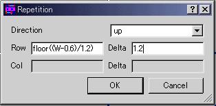
32 Graphical Pcell Functions Add Layer Stretch Repetition

33 Graphical Pcell Parameter Setting
34 Cross-Sectional Viewer for DFM Cross-Sectional Viewer within Expert simulates the cross sectional view of ICs along an arbitrary drawn cut-line on the layout Cross sectional drawings are useful for understanding design rules, parasitic coupling and other design and fabrication problems Design for Manufacturing and Yield Analysis

35 Cross-Sectional Viewer Setup Process simulation parameters Set manually by editing Expert technology file Set interactively using Cross Sectional Viewer setup page of the Expert Preferences dialog panel Layer! {! Name = "NWELL"!...! Material! {!...! Thickness = 4! }!...! Processing! {! ProcessingStep = 1! Operation = DIFFUSE! Undercut = 0! Angle = 100! }! }!

36 Cross-Sectional Viewer for DFM and Yield Analysis Cut Line in Expert Mirrors Cell View In Cross Section View

37 Cross-Sectional Viewer Access Docking Window Cross Section adds, deletes and chooses viewing Multiple Cut Cross-Sectional Viewer enables: View the fabrication processes one step at time Choose first, last, next, and previous fabrication step Zoom current cross section view for convenient investigation of specific sections
38 Conclusion Expert Layout Editor creates all-angle polygons for analog, RF, and microwave circuit elements, including inductors and power devices in CMOS, Bipolar, BiCMOS, SiGe, GaAs, SiC, InP, TFT, and other process technologies Expert Layout Editor enables mask designers to achieve maximum density and performance in analog and digital layouts
PDK-Based Analog/Mixed-Signal/RF Design Flow 11/17/05
 PDK-Based Analog/Mixed-Signal/RF Design Flow 11/17/05 Silvaco s What is a PDK? Which people build, use, and support PDKs? How do analog/mixed-signal/rf engineers use a PDK to design ICs? What is an analog/mixed-signal/rf
Virtuoso Custom Design Platform GXL. Open Database. PDKs. Constraint Management. Customer IP
 Virtuoso Custom Design Platform GL The Cadence Virtuoso custom design platform is the industry s leading design system for complete front-to-back analog, RF, mixed-signal, and custom digital design. The
DATASHEET VIRTUOSO LAYOUT SUITE GXL
 DATASHEET Part of the Cadence Virtuoso Layout Suite family of products, is a collection of fully automated layout capabilities such as custom placement and routing, layout optimization, module generation,
Virtuoso Layout Suite XL
 Accelerated full custom IC layout Part of the Cadence Virtuoso Layout Suite family of products, is a connectivity- and constraint-driven layout environment built on common design intent. It supports custom
Guardian NET Layout Netlist Extractor
 Outline What is Guardian NET Key Features Running Extraction Setup Panel Layout Annotation Layout Text Extraction Node Naming Electric Rule Checking (ERC) Layout Hierarchy Definition Hierarchy Checker
MEMS Pro v5.1 Layout Tutorial Physical Design Mask complexity
 MEMS Pro v5.1 Layout Tutorial 1 Physical Design Mask complexity MEMS masks are complex with curvilinear geometries Verification of manufacturing design rules is important Automatic generation of mask layout
DATASHEET VIRTUOSO LAYOUT SUITE FAMILY
 DATASHEET The Cadence Virtuoso Layout Suite family of products delivers a complete solution for front-to-back custom analog, digital, RF, and mixed-signal design. It preserves design intent throughout
VLSI Lab Tutorial 3. Virtuoso Layout Editing Introduction
 VLSI Lab Tutorial 3 Virtuoso Layout Editing Introduction 1.0 Introduction The purpose of this lab tutorial is to guide you through the design process in creating a custom IC layout for your CMOS inverter
Laker 3 Custom Design Tools
 Datasheet Laker 3 Custom Design Tools Laker 3 Custom Design Tools The Laker 3 Custom Design Tools form a unified front-to-back environment for custom circuit design and layout. They deliver a complete
HIPEX Full-Chip Parasitic Extraction. Summer 2004 Status
 HIPEX Full-Chip Parasitic Extraction Summer 2004 Status What is HIPEX? HIPEX Full-Chip Parasitic Extraction products perform 3D-accurate and 2D-fast extraction of parasitic capacitors and resistors from
Design rule illustrations for the AMI C5N process can be found at:
 Cadence Tutorial B: Layout, DRC, Extraction, and LVS Created for the MSU VLSI program by Professor A. Mason and the AMSaC lab group. Revised by C Young & Waqar A Qureshi -FS08 Document Contents Introduction
electronic lab 11 Fedora Electronic Lab empowers hardware engineers and universities with opensource solutions for micro nano electronics engineering.
 The Fedora Project is out front for you, leading the advancement of free, open software and content. electronic lab 11 Community Leader in opensource EDA deployment Fedora Electronic Lab empowers hardware
Cadence Tutorial 2: Layout, DRC/LVS and Circuit Simulation with Extracted Parasitics
 Cadence Tutorial 2: Layout, DRC/LVS and Circuit Simulation with Extracted Parasitics Introduction This tutorial describes how to generate a mask layout in the Cadence Virtuoso Layout Editor. Use of DIVA
What s new in MEMS Pro V8.0 Highlights
 Click to edit Master title style 1 What s new in MEMS Pro V8.0 Highlights Click Contents to edit Master title style New platform support File I/O enhancements 3D Modeling enhancements Layout enhancements
A Method to Implement Layout Versus Schematic Check in Integrated Circuits Design Programs
 A Method to Implement Layout Versus Schematic Check in Integrated Circuits Design Programs Radu Gabriel Bozomitu, Daniela Ionescu Telecommunications Department Faculty of Electronics and Telecommunications,
Hipex Full-Chip Parasitic Extraction
 What is Hipex? products perform 3D-accurate and 2D-fast extraction of parasitic capacitors and resistors from hierarchical layouts into hierarchical transistor-level netlists using nanometer process technology
Putting Curves in an Orthogonal World
 Putting Curves in an Orthogonal World Extending the EDA Flow to Support Integrated Photonics Masahiro Shiina October 2018 Traditional IC Design Designers & tool developers have lived in a orthogonal world
Process technology and introduction to physical
 Neuromorphic Engineering II Lab 3, Spring 2014 1 Lab 3 March 10, 2014 Process technology and introduction to physical layout Today you will start to learn to use the Virtuoso layout editor XL which is
EE434 ASIC & Digital Systems. From Layout to SPICE Simulation (Virtuoso, Calibre, HSpice) Spring 2017 Dae Hyun Kim
 Spring 2017 Dae Hyun Kim") EE434 ASIC & Digital Systems From Layout to SPICE Simulation (Virtuoso, Calibre, HSpice) Spring 2017 Dae Hyun Kim daehyun@eecs.wsu.edu 1 Preparation for Lab2 Download the following file into your working
EE434 ASIC & Digital Systems From Layout to SPICE Simulation (Virtuoso, Calibre, HSpice) Spring 2017 Dae Hyun Kim daehyun@eecs.wsu.edu 1 Preparation for Lab2 Download the following file into your working
Adding Curves to an Orthogonal World
 Adding Curves to an Orthogonal World Extending the EDA Flow to Support Integrated Photonics Paul Double July 2018 Traditional IC Design BREXIT AHOY! Designers & tool developers have lived in a orthogonal
UNIVERSITY OF WATERLOO
 UNIVERSITY OF WATERLOO UW ASIC DESIGN TEAM: Cadence Tutorial Description: Part I: Layout & DRC of a CMOS inverter. Part II: Extraction & LVS of a CMOS inverter. Part III: Post-Layout Simulation. The Cadence
Technologies and Tools for µe design
 Technologies and Tools for µe design What can CERN offer -PH-ESE Outline Technologies and Tools Status ASIC Testing infrastructure Packaging common needs 2 1 - ASIC Technologies CMOS 130 and 90 nm RF technologies,
Laker Custom Layout Automation System
 The Laker Custom Layout offers powerful solutions for analog, mixed-signal, memory, and custom digital IC design that address key pain points in the layout process. The Laker layout system provides an
Cadence IC Design Manual
 Cadence IC Design Manual For EE5518 ZHENG Huan Qun Lin Long Yang Revised on May 2017 Department of Electrical & Computer Engineering National University of Singapore 1 P age Contents 1 INTRODUCTION...
ASIC Physical Design Top-Level Chip Layout
 ASIC Physical Design Top-Level Chip Layout References: M. Smith, Application Specific Integrated Circuits, Chap. 16 Cadence Virtuoso User Manual Top-level IC design process Typically done before individual
ELEC451 Integrated Circuit Engineering Using Cadence's Virtuoso Layout Editing Tool
 ELEC451 Integrated Circuit Engineering Using Cadence's Virtuoso Layout Editing Tool Contents Contents 1. General 2. Creating and Working On a Layout o 2.1 Undoing/Re-doing an Action o 2.2 Display Options
EEC 116 Fall 2011 Lab #1 Cadence Schematic Capture and Layout Tutorial
 EEC 116 Fall 2011 Lab #1 Cadence Schematic Capture and Layout Tutorial Dept. of Electrical and Computer Engineering University of California, Davis September 26, 2011 Reading: Rabaey Chapters 1, 2, A,
QUEST 3D RLCG Extraction Depending on Frequency. RF Structures Parasitic Extractor
 QUEST 3D RLCG Extraction Depending on Frequency RF Structures Parasitic Extractor Introduction Type of Simulation Inputs / Outputs Graphical Interface Technology Process Layout Field Solver Output DOE
More information can be found in the Cadence manuals Virtuoso Layout Editor User Guide and Cadence Hierarchy Editor User Guide.
 Chapter 6 Building with Layout This chapter consists of two parts. The first describes the generation of layout views and the second deals with the various tools used for verifying the layout, both physical
FACULTY OF ENGINEERING MULTIMEDIA UNIVERSITY LAB SHEET DIGITAL INTEGRATED CIRCUIT
 FACULTY OF ENGINEERING MULTIMEDIA UNIVERSITY LAB SHEET DIGITAL INTEGRATED CIRCUIT DIC1: Schematic Design Entry, Simulation & Verification DIC2: Schematic Driven Layout Drawing (SDL) Design Rule Check (DRC)
UNIVERSITY OF CALIFORNIA College of Engineering Department of Electrical Engineering and Computer Sciences Lab #2: Layout and Simulation
 UNIVERSITY OF CALIFORNIA College of Engineering Department of Electrical Engineering and Computer Sciences Lab #2: Layout and Simulation NTU IC541CA 1 Assumed Knowledge This lab assumes use of the Electric
take control of your photonics design flow Photonic-Electronic IC design and implementation Pieter Dumon 27/09/2016
 take control of your photonics design flow Photonic-Electronic IC design and implementation Pieter Dumon 27/09/2016 Giving photonic IC designers the same power as electronic IC designers. Make it possible
EE115C Digital Electronic Circuits. Tutorial 4: Schematic-driven Layout (Virtuoso XL)
") EE115C Digital Electronic Circuits Tutorial 4: Schematic-driven Layout (Virtuoso XL) This tutorial will demonstrate schematic-driven layout on the example of a 2-input NAND gate. Simple Layout (that won
EE115C Digital Electronic Circuits Tutorial 4: Schematic-driven Layout (Virtuoso XL) This tutorial will demonstrate schematic-driven layout on the example of a 2-input NAND gate. Simple Layout (that won
Cadence Virtuoso Schematic Design and Circuit Simulation Tutorial
 Cadence Virtuoso Schematic Design and Circuit Simulation Tutorial Introduction This tutorial is an introduction to schematic capture and circuit simulation for ENGN1600 using Cadence Virtuoso. These courses
Comprehensive Place-and-Route Platform Olympus-SoC
 Comprehensive Place-and-Route Platform Olympus-SoC Digital IC Design D A T A S H E E T BENEFITS: Olympus-SoC is a comprehensive netlist-to-gdsii physical design implementation platform. Solving Advanced
TUTORIAL II ECE 555 / 755 Updated on September 11 th 2006 CADENCE LAYOUT AND PARASITIC EXTRACTION
 TUTORIAL II ECE 555 / 755 Updated on September 11 th 2006 CADENCE LAYOUT AND PARASITIC EXTRACTION After finishing a schematic of your design (Tutorial-I), the next step is creating masks which are for
AMS DESIGN METHODOLOGY
 OVER VIEW CADENCE ANALOG/ MIXED-SIGNAL DESIGN METHODOLOGY The Cadence Analog/Mixed-Signal (AMS) Design Methodology employs advanced Cadence Virtuoso custom design technologies and leverages silicon-accurate
TQPED MMIC Design Training
 TQPED MMIC Design Training Outline Installation and Use of the Library AWR AWR Design Kit (PDK Process Design Kit) ICED Layout Kit Create a new document using the Library Environment Setup Hotkeys Background
Virtuoso Layout Editor
 This tutorial will cover the basic steps involved in using the Cadence layout editor called Virtuoso, extracting layout, and running simulation on the layout. The inverter layout is used as an example
Galaxy Custom Designer LE Custom Layout Editing
 Datasheet Galaxy Custom Designer LE Custom Layout Editing Overview Galaxy Custom Designer LE is the modern-era choice for layout entry and editing, enabling users to meet the challenges of today s fast-moving
Virtuoso System Design Platform Unified system-aware platform for IC and package design
 Unified system-aware platform for IC and package design The Cadence Virtuoso System Design Platform is a holistic, system-based solution that provides the functionality to drive simulation and LVS-clean
Concurrent, OA-based Mixed-signal Implementation
 Concurrent, OA-based Mixed-signal Implementation Mladen Nizic Eng. Director, Mixed-signal Solution 2011, Cadence Design Systems, Inc. All rights reserved worldwide. Mixed-Signal Design Challenges Traditional
Joe Civello ADS Product Manager/ Keysight EEsof EDA
 Joe Civello 2018.01.11 ADS Product Manager/ Keysight EEsof EDA 3D Layout Viewing directly from the Layout Window 3D Editing & Routing PCB & IC/Module Design Dramatically Improved Visual Inspection Simplified
Galaxy Custom Designer SE The New Choice in Custom Schematic Editing and Simulation Environment
 Datasheet Galaxy Custom Designer SE The New Choice in Custom Schematic Editing and Simulation Environment Overview Galaxy Custom Designer SE is the next-generation choice for schematic entry, enabling
Virtuoso - Enabled EPDA framework AIM SUNY Process
 Virtuoso - Enabled EPDA framework AIM SUNY Process CADENCE, LUMERICAL, PHOENIX SOFTWARE Driven by our customers Cadence is the leader with Virtuoso custom design platform for electronics custom and mixed
O N C A D E N C E V I R T U O S O. CHEN, Jason Application Engineer, Keysight Technologies
 O N C A D E N C E V I R T U O S O CHEN, Jason 2018.05.08 Application Engineer, Keysight Technologies Introduction to Momentum Momentum Features for RFIC Design Circuit/EM Cosimulation Flow on Cadence Virtuoso
DEVELOPMENT OF PARAMETERIZED CELL OF SPIRAL INDUCTOR USING SKILL LANGUAGE
 DEVELOPMENT OF PARAMETERIZED CELL OF SPIRAL INDUCTOR USING SKILL LANGUAGE Vladimir Emilov Grozdanov 1, Diana Ivanova Pukneva 1, Marin Hristov Hristov 2 1 Smartcom, 7 th km, Tzarigradsko Chausee Blvd, 1784
Prepared by Dr. Ulkuhan Guler GT-Bionics Lab Georgia Institute of Technology
 Prepared by Dr. Ulkuhan Guler GT-Bionics Lab Georgia Institute of Technology OUTLINE Introduction Mapping for Schematic and Layout Connectivity Generate Layout from Schematic Connectivity Some Useful Features
Microelectronica. Full-Custom Design with Cadence Tutorial
 Área Científica de Electrónica Microelectronica Full-Custom Design with Cadence Tutorial AustriaMicroSystems C35B3 (HIT-Kit 3.70) Marcelino Santos Table of contends 1. Starting Cadence... 3 Starting Cadence
SILVACO. An Intuitive Front-End to Effective and Efficient Schematic Capture Design INSIDE. Introduction. Concepts of Scholar Schematic Capture
 TCAD Driven CAD A Journal for CAD/CAE Engineers Introduction In our previous publication ("Scholar: An Enhanced Multi-Platform Schematic Capture", Simulation Standard, Vol.10, Number 9, September 1999)
Microwave Office Training
 Microwave Office Training Schematic Layout Schematic Layout Schematic View Circuit We are Here! Schematic Layout View External World Need Export Mapping Two views of the same circuit! - including connectivity
TABLE OF CONTENTS 1.0 PURPOSE INTRODUCTION ESD CHECKS THROUGHOUT IC DESIGN FLOW... 2
 TABLE OF CONTENTS 1.0 PURPOSE... 1 2.0 INTRODUCTION... 1 3.0 ESD CHECKS THROUGHOUT IC DESIGN FLOW... 2 3.1 PRODUCT DEFINITION PHASE... 3 3.2 CHIP ARCHITECTURE PHASE... 4 3.3 MODULE AND FULL IC DESIGN PHASE...
CMOS Design Lab Manual
 CMOS Design Lab Manual Developed By University Program Team CoreEl Technologies (I) Pvt. Ltd. 1 Objective Objective of this lab is to learn the Mentor Graphics HEP2 tools as well learn the flow of the
Harmony-AMS Analog/Mixed-Signal Simulator
 Harmony-AMS Analog/Mixed-Signal Simulator Yokohama, June 2004 Workshop 7/15/04 Challenges for a True Single-Kernel A/MS Simulator Accurate partition of analog and digital circuit blocks Simple communication
Ansys Designer RF Training Lecture 2: Introduction to the Designer GUI
 Ansys Designer RF Solutions for RF/Microwave Component and System Design 7. 0 Release Ansys Designer RF Training Lecture 2: Introduction to the Designer GUI Ansoft Designer Desktop Menu bar Toolbars Schematic
ECE425: Introduction to VLSI System Design Machine Problem 3 Due: 11:59pm Friday, Dec. 15 th 2017
 ECE425: Introduction to VLSI System Design Machine Problem 3 Due: 11:59pm Friday, Dec. 15 th 2017 In this MP, you will use automated tools to synthesize the controller module from your MP2 project into
Calibre Fundamentals: Writing DRC/LVS Rules. Student Workbook
 DRC/LVS Rules Student Workbook 2017 Mentor Graphics Corporation All rights reserved. This document contains information that is trade secret and proprietary to Mentor Graphics Corporation or its licensors
Improve Reliability With Accurate Voltage-Aware DRC. Matthew Hogan, Mentor Graphics
 Improve Reliability With Accurate Voltage-Aware DRC Matthew Hogan, Mentor Graphics BACKGROUND Consumer expectations for longer device operations at sustained performance levels means designing for reliability
EE 330 Laboratory Experiment Number 11
 EE 330 Laboratory Experiment Number 11 Design and Simulation of Digital Circuits using Hardware Description Languages Fall 2017 Contents Purpose:... 3 Background... 3 Part 1: Inverter... 4 1.1 Simulating
Verifying the Multiplexer Layout
 4 This chapter introduces you to interactive verification. You will perform two different tests in the Virtuoso layout editor while using Assura interactive verification products. One test uses the Design
Will Silicon Proof Stay the Only Way to Verify Analog Circuits?
 Will Silicon Proof Stay the Only Way to Verify Analog Circuits? Pierre Dautriche Jean-Paul Morin Advanced CMOS and analog. Embedded analog Embedded RF 0.5 um 0.18um 65nm 28nm FDSOI 0.25um 0.13um 45nm 1997
Detailed Presentation
 Detailed Presentation PDK Leadership - Developing and Delivering High Quality PDKs Simucad PDKs are being rapidly adopted worldwide by leading foundries and design houses because of their quality and ease
Altium Designer Viewer. Contents
 Altium Designer Viewer Contents What You can do Key Features at-a-glance Supported Output Generation Viewer Environment Viewing Schematic Documents Viewing PCB Documents Searching Live Supplier Data Using
Logging in, starting a shell tool, and starting the Cadence Tool Suite
 EEE 4134 VLSI I Laboratory Lab 0 (Introductory Lab) Logging into Cadence Server, Tool Setup, Cell Library Creation, Introduction to Custom IC Design flow Objectives: To login, start a shell tool and start
Design software and services for the integrated photonics market IPKISS Moves the edges in PIC PDK building
 Design software and services for the integrated photonics market IPKISS 3.1.3 Moves the edges in PIC PDK building take controltake of your control photonics of your photonics design flow design flow 1
Computer-Based Project on VLSI Design Co 3/7
 Computer-Based Project on VLSI Design Co 3/7 IC Layout and Symbolic Representation This pamphlet introduces the topic of IC layout in integrated circuit design and discusses the role of Design Rules and
AccuCore STA DSPF Backannotation Timing Verification Design Flow
 Application Note AccuCore STA DSPF Backannotation Timing Verification Design Flow Abstract This application note highlights when and why DSPF backannotation is needed during timing verification, and details
Spiral 2-8. Cell Layout
 2-8.1 Spiral 2-8 Cell Layout 2-8.2 Learning Outcomes I understand how a digital circuit is composed of layers of materials forming transistors and wires I understand how each layer is expressed as geometric
Cadence Rapid Adoption Kits
 Cadence Rapid Adoption Kits Rapid Adoption Kits demonstrate how users can use their tools in their flows to improve productivity and to maximize the benefits of their tools. These packages can contain
Allegro Design Authoring
 Create design intent with ease for simple to complex designs Systems companies looking to create new products at the lowest possible cost need a way to author their designs with ease in a shorter, more
AWR. White Paper. Exactly How Electromagnetic Should Be Part of a Design Flow! introduction
 Extract Flow introduction Modern RF/microwave design flows make extensive use of electromagnetic (EM) analysis in many ways, and its co-existence and concurrency with circuit design and analysis can not
Magic Tutorial #9: Format Conversion for CIF and Calma
 Magic Tutorial #9: Format Conversion for CIF and Calma John Ousterhout Computer Science Division Electrical Engineering and Computer Sciences University of California Berkeley, CA 94720 (Updated by others,
SmartSpice Analog Circuit Simulator Product Update. Yokohama, June 2004 Workshop
 SmartSpice Analog Circuit Simulator Product Update Yokohama, June 2004 Workshop Agenda SmartSpice Products SmartSpice General Features SmartSpice New GUI SmartSpice New features Supported Models and Modeling
VLSI Lab Tutorial 1. Cadence Virtuoso Schematic Composer Introduction
 VLSI Lab Tutorial 1 Cadence Virtuoso Schematic Composer Introduction 1.0 Introduction The purpose of the first lab tutorial is to help you become familiar with the schematic editor, Virtuoso Schematic
DOWNLOAD PDF CADENCE WAVEFORM CALCULATOR USER GUIDE
 Chapter 1 : CSE / Cadence Tutorial The Cadence Design Communities support Cadence users and technologists interacting to exchange ideas, news, technical information, and best practices to solve problems
Professor Muller Fall 2016 Sameet Ramakrishnan Eric Chang Adapted from prior EE140 and EE141 labs. EE 140/240A Lab 0 Full IC Design Flow
 Professor Muller Fall 2016 Sameet Ramakrishnan Eric Chang Adapted from prior EE140 and EE141 labs EE 140/240A Lab 0 Full IC Design Flow In this lab, you will walk through the full process an analog designer
ALLEGRO DESIGN ENTRY HDL 610
 DATASHEET ALLEGRO DESIGN ENTRY HDL 610 ROBUST AND HIGHLY INTEGRATED SCHEMATIC DESIGN Cadence Allegro Design Entry HDL 610, a 600 series product within the Allegro system interconnect design platform, offers
ECE471/571 Energy Efficient VLSI Design Project 2 Cadence Setup and Creation of an Inverter Due Date 11:30 am on Friday, February 2 nd, 2018
 ECE471/571 Energy Efficient VLSI Design Project 2 Cadence Setup and Creation of an Inverter Due Date 11:30 am on Friday, February 2 nd, 2018 Introduction This project will first walk you through the setup
MEMS Pro V3 Layout Tutorial
 MEMS Pro V3 Layout Tutorial MEMSCAP Yiching Liang March 6, 2002 Launching MEMS Pro V3 Double click on the MEMS Pro V3 icon on your desktop to launch MEMS Pro Menu bar Standard toolbar Drawing toolbar SPR/BPR
Advanced Design System Netlist Exporter
 Advanced Design System 2002 Netlist Exporter February 2002 Notice The information contained in this document is subject to change without notice. Agilent Technologies makes no warranty of any kind with
CircuitsMulti-Projets
 From layout to chips CircuitsMulti-Projets MPW Services Center for ICs, Photonics & MEMS Prototyping & Low Volume Production mycmp.fr Grenoble - France From layout to chips STMicroelectronics Standard
DIGITAL CIRCUIT SIMULATOR. Project Proposal
 REVISION REV DESCRIPTION DATE 1.1 Initial Revision 06.10.2005 DIGITAL CIRCUIT SIMULATOR Project Proposal Number of Pages Doc 12 Appendixes A B C D E F G H STARSOFT Middle East Technical University 06531
ESE570 Spring University of Pennsylvania Department of Electrical and System Engineering Digital Integrated Cicruits AND VLSI Fundamentals
 University of Pennsylvania Department of Electrical and System Engineering Digital Integrated Cicruits AND VLSI Fundamentals ESE570, Spring 2019 HW5: Delay and Layout Sunday, February 17th Due: Friday,
ESE 570 Cadence Lab Assignment 2: Introduction to Spectre, Manual Layout Drawing and Post Layout Simulation (PLS)
") ESE 570 Cadence Lab Assignment 2: Introduction to Spectre, Manual Layout Drawing and Post Layout Simulation (PLS) Objective Part A: To become acquainted with Spectre (or HSpice) by simulating an inverter,
ESE 570 Cadence Lab Assignment 2: Introduction to Spectre, Manual Layout Drawing and Post Layout Simulation (PLS) Objective Part A: To become acquainted with Spectre (or HSpice) by simulating an inverter,
PADS-PowerPCB 4 Tutorial (with Blazeroute)
") PADS-PowerPCB 4 Tutorial (with Blazeroute) PADS-PowerPCB is the ultimate design environment for complex, high-speed printed circuit boards. PROCEDURE FOR SIMULATION IN SCHEMATICS 1. Importing Design Data
PADS-PowerPCB 4 Tutorial (with Blazeroute) PADS-PowerPCB is the ultimate design environment for complex, high-speed printed circuit boards. PROCEDURE FOR SIMULATION IN SCHEMATICS 1. Importing Design Data
Using Sonnet in a Cadence Virtuoso Design Flow
 Using Sonnet in a Cadence Virtuoso Design Flow Purpose of this document: This document describes the Sonnet plug-in integration for the Cadence Virtuoso design flow, for silicon accurate EM modelling of
Physical Verification Challenges and Solution for 45nm and Beyond. Haifang Liao Celesda Design Solutions, Inc.
 Physical Verification Challenges and Solution for 45nm and Beyond Haifang Liao Celesda Design Solutions, Inc. Nanometer Design Era Semiconductor feature size has been shrunk 500x in 40 years Space for
What s New in PADS
 What s New in PADS 2007.4 Copyright Mentor Graphics Corporation 2008 All Rights Reserved. Mentor Graphics, Board Station, ViewDraw, Falcon Framework, IdeaStation, ICX and Tau are registered trademarks
OpenAccess PCells Ed Petrus VP Engineering V2
 OpenAccess PCells Ed Petrus VP Engineering V2 April 2005 Page 1 Copyright 2005 CiraNova, Inc. What is CiraNova about? 4 CiraNova enables analog designers to create migratable, re-usable analog objects
OpenPDK Production Value and Benchmark Results
 OpenPDK Production Value and Benchmark Results Philippe MAGARSHACK Executive Vice-President, Design Enablement and Services June 2 nd, 2014 ST s Strong technology portfolio : Several R&D Partnerships &
Tanner Analog Front End Flow. Student Workbook
 Student Workbook 2016 Mentor Graphics Corporation All rights reserved. This document contains information that is trade secret and proprietary to Mentor Graphics Corporation or its licensors and is subject
Design Solutions in Foundry Environment. by Michael Rubin Agilent Technologies
 Design Solutions in Foundry Environment by Michael Rubin Agilent Technologies Presenter: Michael Rubin RFIC Engineer, R&D, Agilent Technologies former EDA Engineering Manager Agilent assignee at Chartered
EE 330 Spring 2018 Laboratory 2: Basic Boolean Circuits
 EE 330 Spring 2018 Laboratory 2: Basic Boolean Circuits Contents Objective:... 2 Part 1: Introduction... 2 Part 2 Simulation of a CMOS Inverter... 3 Part 2.1 Attaching technology information... 3 Part
Cadence Tutorial A: Schematic Entry and Functional Simulation Created for the MSU VLSI program by Andrew Mason and the AMSaC lab group.
 Cadence Tutorial A: Schematic Entry and Functional Simulation Created for the MSU VLSI program by Andrew Mason and the AMSaC lab group. Revision Notes: Aug. 2003 update and edit A. Mason add intro/revision/contents
Welcome to Constraint Manager
 1 Allegro Constraint Manager User Guide 1 Welcome to Constraint Manager Topics in this chapter include The Allegro Constraint Manager Information Set What is Allegro Constraint Manager? Accessing Constraint
CECOS University Department of Electrical Engineering. Wave Propagation and Antennas LAB # 1
 CECOS University Department of Electrical Engineering Wave Propagation and Antennas LAB # 1 Introduction to HFSS 3D Modeling, Properties, Commands & Attributes Lab Instructor: Amjad Iqbal 1. What is HFSS?
GraphWorX64 Productivity Tips
 Description: Overview of the most important productivity tools in GraphWorX64 General Requirement: Basic knowledge of GraphWorX64. Introduction GraphWorX64 has a very powerful development environment in
OpenDFM Targeting Functions. Bob Sayah June 6, 2011 IBM Corporation Si2 Targeting Working Group Chair
 OpenDFM Targeting Functions Bob Sayah June 6, 2011 IBM Corporation Si2 Targeting Working Group Chair Targeting Design Drawn Shapes Mfg. Targeting Targeting takes the Drawn Shapes provided by the layout
Virtuoso Schematic Composer
 is a schematic design tool from Cadence. In this tutorial you will learn how to put electrical components, make wire connections, insert pins and check for connection error. Start Cadence Custom IC Design
CMOS VLSI Design Lab 4: Full Chip Assembly
 CMOS VLSI Design Lab 4: Full Chip Assembly In this final lab, you will assemble and simulate your entire MIPS microprocessor! You will build your top level chip cell by connecting the datapath, aludec,