and 32 bit for 32 bit. If you don t pay attention to this, there will be unexpected behavior in the ISE software and thing may not work properly!
|
|
|
- Janis Shaw
- 5 years ago
- Views:
Transcription
1 This tutorial will show you how to: Part I: Set up a new project in ISE 14.7 Part II: Implement a function using Schematics Part III: Simulate the schematic circuit using ISim Part IV: Constraint, Synthesize, Implement, Generate, and Program for Nexys 3 FPGA board Part I: Set up a new project in Xilinx ISE 14.7 Attention: Make sure to use the appropriate version of the ISE, 64 bit navigator for a 64 bit OS, and 32 bit for 32 bit. If you don t pay attention to this, there will be unexpected behavior in the ISE software and thing may not work properly! 1. Open the Xilinx ISE Design Suit You can click on the ISE icon on the desktop, or search Start All Programs Xilinx ISE Design Suite 14.7 ISE Design Tools Project Navigator The screen should look like the following, the ISE by default opens the last project otherwise none when open first time: 2. Now either press the New Project tab or select File New Project and change the Name and Location to whatever you like. Attention: Xilinx does not allow spaces in path or file names! For example C:\COE 203 will not work, same for the file name! Use the under_score for spaces if you need to. 1

2 The selected Top-level source type: is Schematic because that s what we re planning on using first. This is not critical, as you can always add a new source file of any type later. The dialog box for the project wizard looks like: 3. Click NEXT and in the next dialog box you should fill in the fields as shown here. You can do this in two ways, one is to select an Evaluation Development Board from the drop down list, and in our case you should select Nexys 3. This will automatically fill out the board information in the next five sections. If the board does not exist in the list then you can set correct choices according to the following image. We are using a General Purpose product in the Xilinx Spartan6 family. The specific chip on the Nexys 3 board is an XC6SLX16 in a CSG324 package and the 3 speed grade. Attention: If you fail to set the correct options in this part, you will not be able to implement your design and program it on the Nexys 3 board! Please make sure that the Synthesis Tool is XST, the Simulator is the ISim, and the Preferred Language is Verilog. This is very important for proper operation. 2


3 4. Click NEXT and review the project summary page and then click FINISH, it is always good to double-check the summary to prevent headaches due to the problems you can face while implementing your design if the information is incorrect. Part II: Implement a function using Schematics 3


4 1. Now you should have a new project that targets the correct Xilinx part and other features of the ISE system. Notice the window to the left, and also notice the four tabs Start, Design, Files,, and in the case of an open schematic a Symbols tab will appear. Ensure that the Implementation choice is selected on the design pane. 2. Now you can create a new schematic in your project. Choose Project New Source or right click on the Hierarchy section of the design windows to get the dialog box that adds a new source file to your project (or use the New Source widget on the left vertical tool bar). Source files can be of many types. Select Schematic and name the File name: according to your experiment (here it is simple_logic). Now click NEXT and after observing the summary page click FINISH. 4
5 3. Now you have a blank schematic view, and also a Design Summary view in the main pane of the ISE window. You can switch between windows in the main pane with the tabs along the bottom. The (empty) schematic looks like below. Also note the Hierarchy created and the number of processes such as Synthesis, Implement, Generate, etc. You can run on it. 4. If you don t see this exact view, you may be looking at a different tab in a window. Each pane has tabs at the bottom that let you switch to look at different things. For example, for the left pane in the image above there are multiple tabs to allow different things, Files, Snapshot, Libraries, and Symbols tabs that you can click on and get different information about the project. The lower left pane is the Processes tab and Options tab that show different tools and steps. The main window in the figure above has a simple_logic.sch tab for the new schematic, and a Design Summary tab. If you open more schematics, or other types of files (like Verilog files) the main pane will have additional tabs. Now you can select components from the Symbols tab of the upper left pane and drag them to your schematic. You can narrow down your choices using the Categories, or by typing the first few characters of the symbol you re looking for in the Symbol Name Filter, or just scroll through the lists and see what s there. The important category for now is Logic: General logic gates. 5


6 Grab some components from those categories to make a simple schematic to implement a simple function and drop them into the schematic page. Now we need to add wires and I/O markers by using the tools on the vertical bar between the schematic page and the side pane. Also pay attention to the Options tab at the bottom of the left pane. This section gives you some options on the schematic such as selecting the entire wire branch or selecting line segments. This is good to know if you wanted to only remove a piece of wire and not everything that it is attached to. 5. Use the wiring tool to wire up the components. It is in the tool bar and looks like a red line and a pencil. You could also use Add Wire from the menu. Use the following components (from the Logic category) in this example: a. and2: a two-input AND gate b. or2: a two-input OR gate c. inv: an inverter 6

7 6. Now place I/O Markers to the inputs and outputs. Use the I/O Marker widget that looks like two little labels. You can also use the Add I/O Marker command from the menu. Click on the end points of the wire to add the marker. 7. Always change the name of the marker to a good identifier. Double click the marker, or select the marker and right click to get a menu and choose Edit Properties. Then click on Nets and then edit the Name, also observe the Port Polarity, then click OK. Rename the inputs A, B and C and the output F. An I/O Marker dialog box looks like the following: 7


8 8. Now the resulting schematic looks like the following and it is ready for simulation or synthesis. Once the schematic is saved it should show up in the Sources pane in the upper left of the ISE screen. When you complete your schematic diagram, save it. If there is any error, fix it. Part III: Simulate the schematic circuit using the ISim simulator 8
9 The objective here is to simulate the design to verify its functionality. ISE provides an integrated simulation flow with the ISim simulator that allows simulations to be run from the Xilinx Project Navigator GUI. We introduce the concept of simulation and how to verify the function of a circuit through behavioral simulation. 1. In the project navigator to the left, click on the Design tab, then click on your schematic file. Change to the simulation mode by selecting the Simulation radio button. 2. Press on the + mark in front of ISim Simulator to expand the list. Right click on the Simulate Behavioral Model and choose Process Properties to change simulation attributes. Uncheck the mark in front of Run for Specified Time. This will not limit the simulation for a specific run time. Press OK. 3. To run the simulation, double click on Simulate Behavioral Model, or right click and press Run. 4. ISE will launch ISim in a separate window. Note that the simulation will fail to run if a current process of ISim is working, close any instance of ISim before running any simulation. 5. ISim will launch automatically. The wave window displays the signals, buses and their waveforms. Note that there are four signals shown; A, B, C, and F. 6. Right click on input A in the objects window, and choose Force clock. Add the following values: Leading Edge Value: 0 Trailing Edge Value: 1 Period: 1 us 7. Alternatively, you can write the following Tcl command in the console window: isim force add A 0 -value 1 -time 500 ns -repeat 1 us 8. Similarly, right click on input B in the objects window and choose Force clock. Add the following values: Leading Edge Value: 0 Trailing Edge Value: 1 Period: 0.5 us 9. Alternatively, you can write the Tcl command in the console window: isim force add B 0 -value 1 -radix bin -time 250 ns -value 0 -radix bin -time 500 ns - value 1 -time 750 ns -repeat 1us 10. Similarly, right click on input C in the objects window and choose Force clock. Add the following values: Leading Edge Value: 0 Trailing Edge Value: 1 Period: 0.25 us 11. Enter 1 us inside the simulation time toolbox in the toolbar, and then press Run for the Time Specified in the Toolbar icon. Or type the following Tcl command in the console window. Run 1 us 12. The simulator will show the behavior of the gates according to the specified input signals, press in Zoom to Full View in the toolbar to show the entire simulation period. 13. The simulator will show the behavior of the gates according to the specified input signals, press in Zoom to Full View in the toolbar to show the entire simulation period. You can Zoom in and Zoom out using the icons in the toolbar. 9
. 16.")
10 14. To restart the simulation, press on Restart icon on the toolbar. Note that restarting the simulation will also remove the force clock values. You have to apply force clock to the input signals before running the simulation again. 15. Verify that the circuit is working correctly by checking the time diagram (waveform). 16. Close ISim and return to ISE. Part IV: Constraint, Synthesize, Implement, Generate Bitstream, and Program the Nexys 3 FPGA board Overview: ISE will convert the schematic diagram into a set of configuration bits that are used to program the Xilinx FPGA board. Those configuration bits are in a.bit file and are downloaded to the Xilinx part in this next section of the tutorial. The first three toggle switches on the board for A, B, and C, and the first LED for F is used. UCF (User Constraints File): Because we re headed towards putting this on the Xilinx FPGA on the Nexys 3 board, we need to set some constraints. In particular, we need to tell ISE which pins on the Xilinx chip we want A, B, C, and F assigned to so that we can access those from switches and LEDs on the Nexys 3 board. For that we need a User Constraints File. 10


11 1. First, you need to ensure that you re in the Implementation view by selecting the Implementation radio button on top and that the module you re trying to implement on the board is set as the top module in the top left pane in order to get the options to synthesize, implement, and generate the design. Now if you look at the bottom left pane you can see a number of processes you can run on this schematic top module. 11
 Post-Synthesis.")
12 2. Constraint: Now it starts with creating a floor plan by setting the UCF file. To do this take a look at the User Constraints drop down option in the bottom left pane. We can set the pins in two different ways. Double click on the I/O Pin Planning (Planahead) Post-Synthesis. This should bring up a message box for adding a new UCF file to your design, so click yes and this will kick start another Xilinx tool called Plan Ahead. This program allows you to set all constraints on all I/O pins in the design. Please follow these steps carefully. 3. Pin Assignment: We need to edit the initial UCF for the details of connections between the ports and pins in the design, so as Plan Ahead opens, take a look at the horizontal bottom pane. After expanding the Scalar Ports drop-down you should see all of the I/O pins. Click on the name of the pin (A, B, C, ) and then look at the properties table line listed in front of it. The only property that we want to change is the Site. The Site is the Pin# (FPGA board Pin Identifier). You can find all sorts of the information including the module schematics and the Pin #s for all of the Nexys 3 Peripherals by studying the Nexys 3 manual found at In order to change a property for any port, click on the rectangular space in the correct column and the correct row for the respective port. This click causes a drop-down menu to appear and then you can select the right choice. You can either type or select the correct choice. If there is a choice already selected then clicking on the text will allow you to change it, then hit enter. For the above circuit look for the three switches and an LED, you can also look closely at the actual switch or LED on the board and you will see an identifier in parentheses (i.e. T10 for SW0 referring to Pin #T10 connecting to Switch 0, the first toggle switch from the right). Set the correct identifier to the correct port in your design in Plan Ahead as follows: 12


13 After you re done putting the right Pin # for all the ports in the design, click the SAVE button from the top menu in the page and close down Plan Ahead. And your resulting UCF file should look like the following: 4. Synthesize: Now the design is ready for more processing and the next in line is to synthesize. This process will create a structural representation of the design (similar to compiling C code into assembly code). Do this by first ensuring that the top module is selected and highlighted in the top left pane of ISE and then simply double clicking Synthesize XST in the lower left pane. After the process is done, you will either get a green check mark ( everything is smooth), a yellow attention mark (! there are warnings!), or a red X mark (X there are errors!), and orange question mark (? out of date). In the case of errors you need to investigate them by looking at the Errors tab on the bottom pane and fix, and then re-run synthesis. In the case of warnings make sure to review them and validate they are safe, or in the case of green you re ready for the next step. The synthesis process also creates a couple of more useful things that you should explore and study. One is the synthesis report full of information about timing, resource usage details, and etc. The other is generated RTL schematic; sometimes it is very useful to see what the XST made out of your of schematic. You can view these (highly recommended) by expanding Synthesize XST for the schematic 13
, double click the Implement Design process in the Processes tab.")
14 and the Design Summary page in the main pane for the report. 5. Implement: Next step is to define the hardware configuration. With your top module source file selected (simple_verilog.sch in this case), double click the Implement Design process in the Processes tab. This will translate the design to something that can physically be mapped to the particular FPGA that s on our board (the xc6slx16-3csg324). You should see a green check mark if this step finishes without issues. If there are issues, you need to read them for clues about what went wrong and what you should look at to fix things. If you expand this Implement Design tab (which is not necessary) you will see that the Implement Design process actually consists of three parts: a) Translate: Translate is the first step in the implementation process. The Translate process merges all of the input netlists and design constraint information and outputs a Xilinx NGD (Native Generic Database) file. The output NGD file can then be mapped to the targeted FPGA device. b) Map: Mapping is the process of assigning a design s logic elements to the specific physical elements that actually implement logic functions in a device. The Map process creates an NCD (Native Circuit Description) file. The NCD file will be used by the PAR process. c) Place and Route (PAR): PAR uses the NCD file created by the Map process to place and route your design. PAR outputs an NCD file that is used by the bitstream generator (BitGen) to create a (.bit) file. The Bit file (see the next step) is what s used to actually program the FPGA. In this part the actual transistor configuration and wire routing is decided. 14


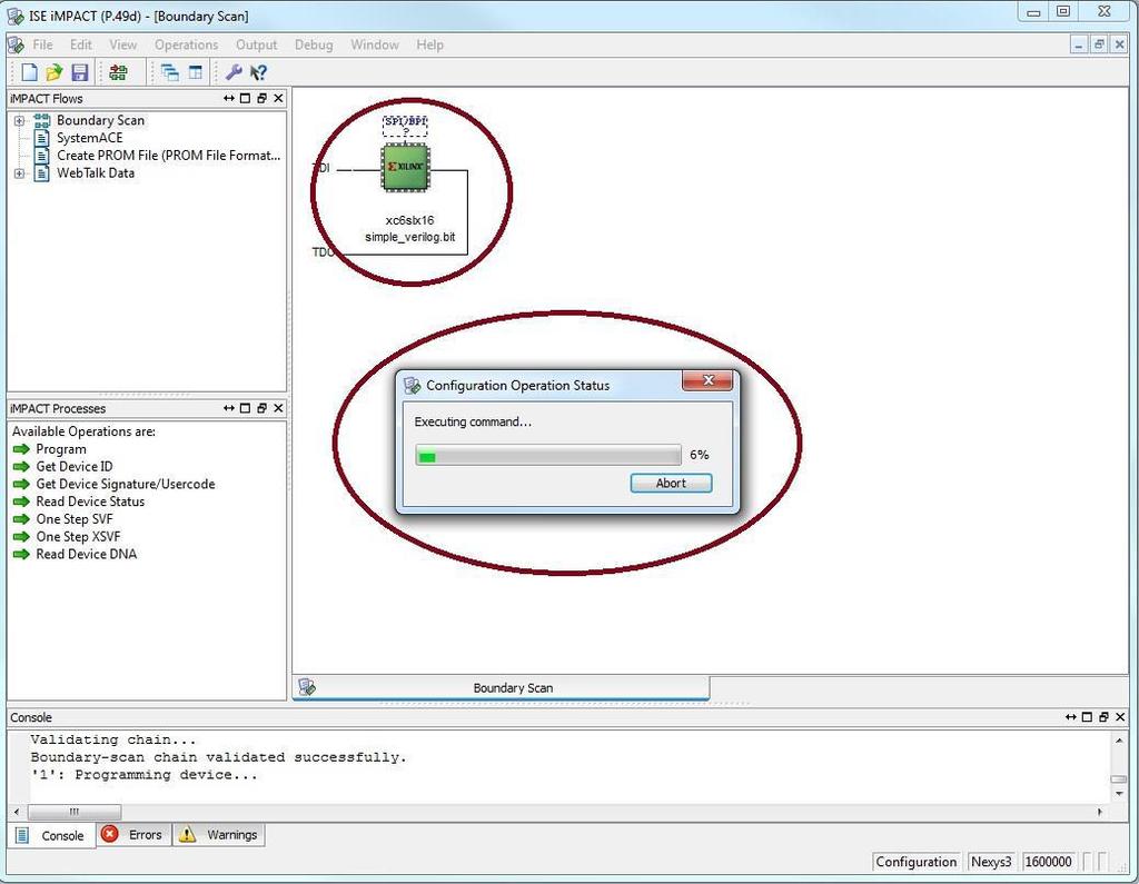
15 6. Generate: In this step all information resulting from the previous steps are gathered and put into a Bit format that the USB programmer on the FPGA board (in our case Nexys3) understands. Simply double-click the Generate Programming File to generate a.bit file which will be used in the final step to program the board. Now the design is ready to be put on the board so we can physically see its functionality. Attention: Before proceeding to the next step connect the board via the USB cable to the PC you re using, and turn on the power, the next step ensure proper connection to the board. Also note that you do not have to do steps 4, 5, and 6 individually. These processes are dependent on each other, if one needs a preceding process to be updated then it will automatically run that process before it runs itself. So you can just proceed to step 7 and watch ISE do everything. 7. Program: You can start the programming process by double clicking Configure Target Device and ISE will launch yet another Xilinx tool called impact. A warning box appears complaining about No impact project file exists, so just click OK to launch impact as it will automatically read your existing project. 8. In the ISE impact window which again looks a lot like ISE, double click Boundary Scan in the top left pane. In the boundary scan windows in the main pane, where it says Right click to Add Device or Initialize chain right-click in the middle of the page and select Initialize Chain or just press Ctrl + I. This will ensure there is a good connection to your board and it can communicate with it. 15


16 9. After impact verifies that the cable is connected it will prompt you to load your.bit file that you generated in step 6. Note that this file selection window doesn t always default to your existing project so you may need to navigate to your project folder and locate the.bit file. This file is always named to your top module so in our case it is simple_verilog.bit. Double-click or select the bit file and click open, again make sure it is the right file. 16


17 10. After the bit file is read in, impact prompts you to attach a PROM controller, just click NO to skip this step since we re not putting anything in the Flash memory. 11. In the next dialog box you would be verifying which device on the board you re targeting but in our case we only have the FPGA chip to program, so click Ok and the preparation for programming the board is complete. 12. All that is left is to right click on the green chip icon with the Xilinx logo in the main pane and click Program. After the communication bar finishes, your design is programmed to the Nexys 3 FPGA board. When the program operation completes, a blue message with Program Succeeded appears. 17
18 18
Tutorial: Working with the Xilinx tools 14.4
 Tutorial: Working with the Xilinx tools 14.4 This tutorial will show you how to: Part I: Set up a new project in ISE Part II: Implement a function using Schematics Part III: Implement a function using
Tutorial: ISE 12.2 and the Spartan3e Board v August 2010
 Tutorial: ISE 12.2 and the Spartan3e Board v12.2.1 August 2010 This tutorial will show you how to: Use a combination of schematics and Verilog to specify a design Simulate that design Define pin constraints
Getting started with the Xilinx Project Navigator and the Digilent BASYS 2 board.
 Getting started with the Xilinx Project Navigator and the Digilent BASYS 2 board. This lab is based on: Xilinx Project Navigator, Release Version 14.6 Digilent Adept System Rev 2.7, Runtime Rev 2.16 Digilent
Tutorial: Working with Verilog and the Xilinx FPGA in ISE 9.2i
 Tutorial: Working with Verilog and the Xilinx FPGA in ISE 9.2i This tutorial will show you how to: Use Verilog to specify a design Simulate that Verilog design Define pin constraints for the FPGA (.ucf
EE 1315 DIGITAL LOGIC LAB EE Dept, UMD
 EE 1315 DIGITAL LOGIC LAB EE Dept, UMD EXPERIMENT # 1: Logic building blocks The main objective of this experiment is to let you familiarize with the lab equipment and learn about the operation of the
Introduction. About this tutorial. How to use this tutorial
 Basic Entry & not About this tutorial This tutorial consists of an introduction to creating simple circuits on an FPGA using a variety of methods. There are two ways to create the circuit: using or by
Xilinx Tutorial Basic Walk-through
 Introduction to Digital Logic Design with FPGA s: Digital logic circuits form the basis of all digital electronic devices. FPGAs (Field Programmable Gate Array) are large programmable digital electronic
Circuit design with configurable devices (FPGA)
") 1 Material Circuit design with configurable devices (FPGA) Computer with Xilinx's ISE software installed. Digilent's Basys2 prototype board and documentation. Sample design files (lab kit). Files and documents
1 Material Circuit design with configurable devices (FPGA) Computer with Xilinx's ISE software installed. Digilent's Basys2 prototype board and documentation. Sample design files (lab kit). Files and documents
Revision: February 27, E Main Suite D Pullman, WA (509) Voice and Fax
 Voice and Fax") Xilinx ISE WebPACK Schematic Capture Tutorial Revision: February 27, 2010 215 E Main Suite D Pullman, WA 99163 (509) 334 6306 Voice and Fax Overview This tutorial provides instruction for using the Xilinx
Xilinx ISE WebPACK Schematic Capture Tutorial Revision: February 27, 2010 215 E Main Suite D Pullman, WA 99163 (509) 334 6306 Voice and Fax Overview This tutorial provides instruction for using the Xilinx
ECE 4305 Computer Architecture Lab #1
 ECE 4305 Computer Architecture Lab #1 The objective of this lab is for students to familiarize with the FPGA prototyping system board (Nexys-2) and the Xilinx software development environment that will
Implementing a Verilog design into the UWEE CPLD Development Board Using Xilinx s ISE 7.1i Software: A Tutorial
 Implementing a Verilog design into the UWEE CPLD Development Board Using Xilinx s ISE 7.1i Software: A Tutorial Revision 0 By: Evan Gander Materials: The following are required in order to complete this
Lab 1: Introduction to Verilog HDL and the Xilinx ISE
 EE 231-1 - Fall 2016 Lab 1: Introduction to Verilog HDL and the Xilinx ISE Introduction In this lab simple circuits will be designed by programming the field-programmable gate array (FPGA). At the end
Xilinx ISE Synthesis Tutorial
 Xilinx ISE Synthesis Tutorial The following tutorial provides a basic description of how to use Xilinx ISE to create a simple 2-input AND gate and synthesize the design onto the Spartan-3E Starter Board
TLL5000 Electronic System Design Base Module
 TLL5000 Electronic System Design Base Module The Learning Labs, Inc. Copyright 2007 Manual Revision 2007.12.28 1 Copyright 2007 The Learning Labs, Inc. Copyright Notice The Learning Labs, Inc. ( TLL )
ELEC 4200 Lab#0 Tutorial
 1 ELEC 4200 Lab#0 Tutorial Objectives(1) In this Lab exercise, we will design and implement a 2-to-1 multiplexer (MUX), using Xilinx Vivado tools to create a VHDL model of the design, verify the model,
TLL5000 Electronic System Design Base Module. Getting Started Guide, Ver 3.4
 TLL5000 Electronic System Design Base Module Getting Started Guide, Ver 3.4 COPYRIGHT NOTICE The Learning Labs, Inc. ( TLL ) All rights reserved, 2008 Reproduction in any form without permission is prohibited.
Xilinx Schematic Entry Tutorial
 Overview Xilinx Schematic Entry Tutorial Xilinx ISE Schematic Entry & Modelsim Simulation What is circuit simulation and why is it important? Complex designs, short design cycle Simultaneous system design
Nexys 2/3 board tutorial (Decoder, ISE 13.2) Jim Duckworth, August 2011, WPI. (updated March 2012 to include Nexys2 board)
 Jim Duckworth, August 2011, WPI. (updated March 2012 to include Nexys2 board)") Nexys 2/3 board tutorial (Decoder, ISE 13.2) Jim Duckworth, August 2011, WPI. (updated March 2012 to include Nexys2 board) Note: you will need the Xilinx ISE Webpack installed on your computer (or you
Nexys 2/3 board tutorial (Decoder, ISE 13.2) Jim Duckworth, August 2011, WPI. (updated March 2012 to include Nexys2 board) Note: you will need the Xilinx ISE Webpack installed on your computer (or you
To practice combinational logic on Logisim and Xilinx ISE tools. ...
 ENGG1203: Introduction to Electrical and Electronic Engineering Second Semester, 2017 18 Lab 1 Objective: To practice combinational logic on Logisim and Xilinx ISE tools. 1 Find your lab partner You will
4. Verify that HDL is selected as the Top-Level Source Type, and click Next. The New Project Wizard Device Properties page appears.
 Working with the GODIL Author: Ruud Baltissen Credits: Michael Randelzhofer, Ed Spittles Date: August 2010 What is it? This document describes a way to get familiar with the Xilinx FPGAs on OHO s Godil,
Nexys 2 board tutorial (Decoder, ISE 12.2) Jim Duckworth, August 2010, WPI. Digilent Adept Programming Steps added by Zoe (Zhu Fu)
 Jim Duckworth, August 2010, WPI. Digilent Adept Programming Steps added by Zoe (Zhu Fu)") Nexys 2 board tutorial (Decoder, ISE 12.2) Jim Duckworth, August 2010, WPI. Digilent Adept Programming Steps added by Zoe (Zhu Fu) Note: you will need the Xlinx ISE Webpack installed on your compuer (or
Nexys 2 board tutorial (Decoder, ISE 12.2) Jim Duckworth, August 2010, WPI. Digilent Adept Programming Steps added by Zoe (Zhu Fu) Note: you will need the Xlinx ISE Webpack installed on your compuer (or
Boise State University Digital Systems Laboratory
 by S. M. Loo, Arlen Planting Department of Electrical and Computer Engineering Boise State University First Released: Spring 2005 with ISE 6.3i Updated: Fall 2006 with ISE 8.1i Updated: Spring 2009 with
Vivado Tutorial. Introduction. Objectives. Procedure. Lab Workbook. Vivado Tutorial
 Lab Workbook Introduction This tutorial guides you through the design flow using Xilinx Vivado software to create a simple digital circuit using Verilog HDL. A typical design flow consists of creating
Banks, Jasmine Elizabeth (2011) The Spartan 3E Tutorial 1 : Introduction to FPGA Programming, Version 1.0. [Tutorial Programme]
![Banks, Jasmine Elizabeth (2011) The Spartan 3E Tutorial 1 : Introduction to FPGA Programming, Version 1.0. [Tutorial Programme]](/thumbs/75/72381729.jpg "Banks, Jasmine Elizabeth (2011) The Spartan 3E Tutorial 1 : Introduction to FPGA Programming, Version 1.0. [Tutorial Programme]") QUT Digital Repository: http://eprints.qut.edu.au/ This is the author version published as: This is the accepted version of this article. To be published as : This is the author s version published as:
QUT Digital Repository: http://eprints.qut.edu.au/ This is the author version published as: This is the accepted version of this article. To be published as : This is the author s version published as:
RTL Design and IP Generation Tutorial. PlanAhead Design Tool
 RTL Design and IP Generation Tutorial PlanAhead Design Tool Notice of Disclaimer The information disclosed to you hereunder (the "Materials") is provided solely for the selection and use of Xilinx products.
UNIVERSITY OF CALIFORNIA, DAVIS Department of Electrical and Computer Engineering. EEC180A DIGITAL SYSTEMS I Winter 2015
 UNIVERSITY OF CALIFORNIA, DAVIS Department of Electrical and Computer Engineering EEC180A DIGITAL SYSTEMS I Winter 2015 LAB 1: Introduction to Quartus II Schematic Capture and ModelSim Simulation This
EE183 LAB TUTORIAL. Introduction. Projects. Design Entry
 EE183 LAB TUTORIAL Introduction You will be using several CAD tools to implement your designs in EE183. The purpose of this lab tutorial is to introduce you to the tools that you will be using, Xilinx
PlanAhead Software Tutorial
 PlanAhead Software Tutorial RTL Design and IP Generation The information disclosed to you hereunder (the Information ) is provided AS-IS with no warranty of any kind, express or implied. Xilinx does not
Xilinx ISE/WebPack: Introduction to Schematic Capture and Simulation
 Xilinx ISE/WebPack: Introduction to Schematic Capture and Simulation Revision: February 7, 2003 Overview This document is intended to assist new entry-level users of the Xilinx ISE/WebPack software. It
Quick Front-to-Back Overview Tutorial
 Quick Front-to-Back Overview Tutorial PlanAhead Design Tool This tutorial document was last validated using the following software version: ISE Design Suite 14.5 If using a later software version, there
ISE Simulator (ISim) In-Depth Tutorial. UG682 (v 13.1) March 1, 2011
 In-Depth Tutorial. UG682 (v 13.1) March 1, 2011") ISE Simulator (ISim) In-Depth Tutorial Xilinx is disclosing this user guide, manual, release note, and/or specification (the "Documentation") to you solely for use in the development of designs to operate
ISE Simulator (ISim) In-Depth Tutorial Xilinx is disclosing this user guide, manual, release note, and/or specification (the "Documentation") to you solely for use in the development of designs to operate
Circuit Design and Simulation with VHDL 2nd edition Volnei A. Pedroni MIT Press, 2010 Book web:
 Circuit Design and Simulation with VHDL 2nd edition Volnei A. Pedroni MIT Press, 2010 Book web: www.vhdl.us Appendix C Xilinx ISE Tutorial (ISE 11.1) This tutorial is based on ISE 11.1 WebPack (free at
Programming Xilinx SPARTAN 3 Board (Simulation through Implementation)
") Programming Xilinx SPARTAN 3 Board (Simulation through Implementation) September 2008 Prepared by: Oluwayomi Adamo Class: Project IV University of North Texas FPGA Physical Description 4 1. VGA (HD-15)
Programming Xilinx SPARTAN 3 Board (Simulation through Implementation) September 2008 Prepared by: Oluwayomi Adamo Class: Project IV University of North Texas FPGA Physical Description 4 1. VGA (HD-15)
Revision: February 27, E Main Suite D Pullman, WA (509) Voice and Fax
 Voice and Fax") Xilinx ISE WebPACK VHDL Tutorial Revision: February 27, 2010 215 E Main Suite D Pullman, WA 99163 (509) 334 6306 Voice and Fax Overview This tutorial provides simple instruction for using the Xilinx ISE
Xilinx ISE WebPACK VHDL Tutorial Revision: February 27, 2010 215 E Main Suite D Pullman, WA 99163 (509) 334 6306 Voice and Fax Overview This tutorial provides simple instruction for using the Xilinx ISE
FPGA Design Flow 1. All About FPGA
 FPGA Design Flow 1 In this part of tutorial we are going to have a short intro on FPGA design flow. A simplified version of FPGA design flow is given in the flowing diagram. FPGA Design Flow 2 FPGA_Design_FLOW
ENGN 1630: CPLD Simulation Fall ENGN 1630 Fall Simulating XC9572XLs on the ENGN1630 CPLD-II Board Using Xilinx ISim
 ENGN 1630 Fall 2018 Simulating XC9572XLs on the ENGN1630 CPLD-II Board Using Xilinx ISim You will use the Xilinx ISim simulation software for the required timing simulation of the XC9572XL CPLD programmable
Vivado Tutorial. Introduction. Objectives. Procedure
 Lab Workbook Introduction This tutorial guides you through the design flow using Xilinx Vivado software to create a simple digital circuit using VHDL. A typical design flow consists of creating model(s),
Getting Started with Xilinx WebPack 13.1
 Getting Started with Xilinx WebPack 13.1 B. Ackland June 2011 (Adapted from S. Tewksbury notes WebPack 7.1) This tutorial is designed to help you to become familiar with the operation of the WebPack software
CECS LAB 1 Introduction to Xilinx EDA Tools
 NAME: DUE DATE: STUDENT ID: POSSIBLE POINTS: 10 COURSE DATE & TIME: OBJECTIVE: To familiarize ourselves with the Xilinx Electronic Design Aid (EDA) Tools. We will simulate a simple 4-to-1 Multiplexor using
The board is powered by the USB connection, so to turn it on or off you plug it in or unplug it, respectively.
 Lab 1 You may work in pairs or individually on this lab Lab Objectives Learn about the equipment we will be using and how to handle it safely. Learn the basics of using Xilinx ISE to develop hardware designs
Xilinx Vivado/SDK Tutorial
 Xilinx Vivado/SDK Tutorial (Laboratory Session 1, EDAN15) Flavius.Gruian@cs.lth.se March 21, 2017 This tutorial shows you how to create and run a simple MicroBlaze-based system on a Digilent Nexys-4 prototyping
Logic Implementation on a Xilinx FPGA using VHDL WWU Linux platform assumed. rev 10/25/16
 1 Logic Implementation on a Xilinx FPGA using VHDL WWU Linux platform assumed. rev 10/25/16 The following is a general outline of steps (i.e. design flow) used to implement a digital system described with
Tutorial on FPGA Design Flow based on Xilinx ISE WebPack and ModelSim. ver. 2.0
 Tutorial on FPGA Design Flow based on Xilinx ISE WebPack and ModelSim ver. 2.0 Updated: Fall 2013 1 Preparing the Input: Download examples associated with this tutorial posted at http://ece.gmu.edu/tutorials-and-lab-manuals
Start Active-HDL. Create a new workspace TUTORIAL #1 CREATING AND SIMULATING SIMPLE SCHEMATICS
 Introduction to Active-HDL TUTORIAL #1 CREATING AND SIMULATING SIMPLE SCHEMATICS This tutorial will introduce the tools and techniques necessary to design a basic schematic. The goal of this tutorial is
Xilinx ISE8.1 and Spartan-3 Tutorial EE3810
 Xilinx ISE8.1 and Spartan-3 Tutorial EE3810 1 Part1) Starting a new project Simple 3-to-8 Decoder Start the Xilinx ISE 8.1i Project Navigator: Select File > New Project in the opened window 2 Select a
Step 1: Downloading the source files
 Introduction: In this lab and in the remainder of the ELEC 2607 labs, you will be using the Xilinx ISE to enter and simulate the designs for your circuits. In labs 3 and 4, you will use ISE to compile
Xilinx ISE8.1 and Spartan-3 Tutorial (Prepared by Kahraman Akdemir based on Professor Duckworth's Tutorials updated September 2006)
") Xilinx ISE8.1 and Spartan-3 Tutorial (Prepared by Kahraman Akdemir based on Professor Duckworth's Tutorials updated September 2006) 1 Part1) Starting a new project Simple 3-to-8 Decoder Start the Xilinx
Xilinx ISE8.1 and Spartan-3 Tutorial (Prepared by Kahraman Akdemir based on Professor Duckworth's Tutorials updated September 2006) 1 Part1) Starting a new project Simple 3-to-8 Decoder Start the Xilinx
2IN35 VLSI Programming Lab Work Assignment 1: Hardware design using Verilog
 2IN35 VLSI Programming Lab Work Assignment 1: Hardware design using Verilog Hrishikesh Salunkhe, h.l.salunkhe@tue.nl, Alok Lele, a.lele@tue.nl April 28, 2015 1 Contents 1 Introduction 3 2 Hardware design
Using Synplify Pro, ISE and ModelSim
 Using Synplify Pro, ISE and ModelSim VLSI Systems on Chip ET4 351 Rene van Leuken Huib Lincklaen Arriëns Rev. 1.2 The EDA programs that will be used are: For RTL synthesis: Synplicity Synplify Pro For
After opening the Programs> Xilinx ISE 8.2i > Project Navigator, you will come to this screen as start-up.
 After opening the Programs> Xilinx ISE 8.2i > Project Navigator, you will come to this screen as start-up. Start with a new project. Enter a project name and be sure to select Schematic as the Top-Level
NOTE: This tutorial contains many large illustrations. Page breaks have been added to keep images on the same page as the step that they represent.
 CSE 352 Tutorial # 4 Synthesizing onto an FPGA Objectives This tutorial will walk you through the steps of implementing a design made in Active-HDL onto the Altera Cyclone II FPGA NOTE: This tutorial contains
PlanAhead Release Notes
 PlanAhead Release Notes What s New in the 11.1 Release UG656(v 11.1.0) April 27, 2009 PlanAhead 11.1 Release Notes Page 1 Table of Contents What s New in the PlanAhead 11.1 Release... 4 Device Support...
EE 367 Logic Design Lab #1 Introduction to Xilinx ISE and the ML40X Eval Board Date: 1/21/09 Due: 1/28/09
 EE 367 Logic Design Lab #1 Introduction to Xilinx ISE and the ML40X Eval Board Date: 1/21/09 Due: 1/28/09 Lab Description Today s lab will introduce you to the Xilinx Integrated Software Environment (ISE)
ISE Design Suite Software Manuals and Help
 ISE Design Suite Software Manuals and Help These documents support the Xilinx ISE Design Suite. Click a document title on the left to view a document, or click a design step in the following figure to
TUTORIAL #2 HIERARCHICAL DESIGNS AND TEST FIXTURES
 Introduction to Active-HDL TUTORIAL #2 HIERARCHICAL DESIGNS AND TEST FIXTURES This tutorial will use the 1-bit full adder you designed in Tutorial #1 to construct larger adders. This will introduce the
PlanAhead Software Tutorial
 PlanAhead Software Tutorial Team Design NOTICE OF DISCLAIMER: The information disclosed to you hereunder (the Information ) is provided AS-IS with no warranty of any kind, express or implied. Xilinx does
Lab 3: Xilinx PicoBlaze Flow Lab Targeting Spartan-3E Starter Kit
 Lab 3: Xilinx PicoBlaze Flow Lab Targeting Spartan-3E Starter Kit Xilinx PicoBlaze Flow Demo Lab www.xilinx.com 1-1 Create a New Project Step 1 Create a new project targeting the Spartan-3E device that
CPLD Experiment 4. XOR and XNOR Gates with Applications
 CPLD Experiment 4 XOR and XNOR Gates with Applications Based on Xilinx ISE Design Suit 10.1 Department of Electrical & Computer Engineering Florida International University Objectives Materials Examining
Digital Systems EEE4084F FPGA Introduction Verilog and Xilinx ISE [30 Marks]
![Digital Systems EEE4084F FPGA Introduction Verilog and Xilinx ISE [30 Marks]](/thumbs/95/125843100.jpg "Digital Systems EEE4084F FPGA Introduction Verilog and Xilinx ISE [30 Marks]") Digital Systems EEE4084F 2017-05-10 FPGA Introduction Verilog and Xilinx ISE [30 Marks] Background This practical is divided into two parts. The first is a tutorial that shows you how to set up a new FPGA
Digital Systems EEE4084F 2017-05-10 FPGA Introduction Verilog and Xilinx ISE [30 Marks] Background This practical is divided into two parts. The first is a tutorial that shows you how to set up a new FPGA
Xilinx Project Navigator Reference Guide
 31 July 2003 Author: David M. Sendek Xilinx Project Navigator Reference Guide Background: This guide provides you with step-by-step procedures in using the Xilinx Project Navigator to perform the following:
Contents. Appendix B HDL Entry Tutorial 2 Page 1 of 14
 Appendix B HDL Entry Tutorial 2 Page 1 of 14 Contents Appendix B HDL Entry Tutorial 2...2 B.1 Getting Started...2 B.1.1 Preparing a Folder for the Project...2 B.1.2 Starting Quartus II...2 B.1.3 Creating
ISim In-Depth Tutorial. UG682 (v13.4) January 18, 2012
 January 18, 2012") ISim In-Depth Tutorial Xilinx is disclosing this user guide, manual, release note, and/or specification (the "Documentation") to you solely for use in the development of designs to operate with Xilinx
ISim In-Depth Tutorial Xilinx is disclosing this user guide, manual, release note, and/or specification (the "Documentation") to you solely for use in the development of designs to operate with Xilinx
Design a three-input, two-output sequential digital circuit which functions as a digital locking mechanism. LOCK ALARM
 Department of Computing Course 112 Hardware First Year Laboratory Assignment Dates for the session 2005-2006: Hand out Date: 10 th January 2006 Hand in deadline (electronic and written report): 17.00 Monday
The Alarm System: The alarm system to be designed has the following inputs.
 1 Introduction In this lab you will use the Xilinx CAD tools to complete the design of a simple home alarm system containing sensors for that indicate whether the Windows, Door, and Garage are secure.
CSE 591: Advanced Hardware Design and Verification (2012 Spring) LAB #0
 LAB #0") Lab 0: Tutorial on Xilinx Project Navigator & ALDEC s Active-HDL Simulator CSE 591: Advanced Hardware Design and Verification Assigned: 01/05/2011 Due: 01/19/2011 Table of Contents 1 Overview... 2 1.1
Lab 0: Tutorial on Xilinx Project Navigator & ALDEC s Active-HDL Simulator CSE 591: Advanced Hardware Design and Verification Assigned: 01/05/2011 Due: 01/19/2011 Table of Contents 1 Overview... 2 1.1
EE 330 Laboratory Experiment Number 11
 EE 330 Laboratory Experiment Number 11 Design and Simulation of Digital Circuits using Hardware Description Languages Fall 2017 Contents Purpose:... 3 Background... 3 Part 1: Inverter... 4 1.1 Simulating
University of Florida EEL 3701 Dr. Eric M. Schwartz Department of Electrical & Computer Engineering Revision 0 12-Jun-16
 Page 1/14 Quartus Tutorial with Basic Graphical Gate Entry and Simulation Example Problem Given the logic equation Y = A*/B + /C, implement this equation using a two input AND gate, a two input OR gate
Adding the ILA Core to an Existing Design Lab
 Adding the ILA Core to an Existing Introduction This lab consists of adding a ChipScope Pro software ILA core with the Core Inserter tool and debugging a nonfunctioning design. The files for this lab are
Tutorial on Quartus II Introduction Using Verilog Code
 Tutorial on Quartus II Introduction Using Verilog Code (Version 15) 1 Introduction This tutorial presents an introduction to the Quartus II CAD system. It gives a general overview of a typical CAD flow
Actel Libero TM Integrated Design Environment v2.3 Structural Schematic Flow Design Tutorial
 Actel Libero TM Integrated Design Environment v2.3 Structural Schematic Flow Design Tutorial 1 Table of Contents Design Flow in Libero TM IDE v2.3 Step 1 - Design Creation 3 Step 2 - Design Verification
Logic Implementation on a Xilinx FPGA using VHDL WWU Linux platform assumed. rev 11/01/17
 1 Logic Implementation on a Xilinx FPGA using VHDL WWU Linux platform assumed. rev 11/01/17 The following is a general outline of steps (i.e. design flow) used to implement a digital system described with
Tutorial on FPGA Design Flow based on Aldec Active HDL. Ver 1.5
 Tutorial on FPGA Design Flow based on Aldec Active HDL Ver 1.5 1 Prepared by Ekawat (Ice) Homsirikamol, Marcin Rogawski, Jeremy Kelly, John Pham, and Dr. Kris Gaj This tutorial assumes that you have basic
MANUAL XILINX ISE PROJECT NAVIGATOR
 Hochschule für Angewandte Wissenschaften Hamburg University of Applied Sciences Department of Electrical Engineering and Computer Sciences MANUAL XILINX ISE PROJECT NAVIGATOR AND MODELSIM Design Flow for
VIVADO TUTORIAL- TIMING AND POWER ANALYSIS
 VIVADO TUTORIAL- TIMING AND POWER ANALYSIS IMPORTING THE PROJECT FROM ISE TO VIVADO Initially for migrating the same project which we did in ISE 14.7 to Vivado 2016.1 you will need to follow the steps
Tutorial - Using Xilinx System Generator 14.6 for Co-Simulation on Digilent NEXYS3 (Spartan-6) Board
 Board") Tutorial - Using Xilinx System Generator 14.6 for Co-Simulation on Digilent NEXYS3 (Spartan-6) Board Shawki Areibi August 15, 2017 1 Introduction Xilinx System Generator provides a set of Simulink blocks
Tutorial - Using Xilinx System Generator 14.6 for Co-Simulation on Digilent NEXYS3 (Spartan-6) Board Shawki Areibi August 15, 2017 1 Introduction Xilinx System Generator provides a set of Simulink blocks
Vivado Design Suite Tutorial. Design Flows Overview
 Vivado Design Suite Tutorial Design Flows Overview Notice of Disclaimer The information disclosed to you hereunder (the "Materials") is provided solely for the selection and use of Xilinx products. To
1. Introduction EE108A. Lab 1: Combinational Logic: Extension of the Tic Tac Toe Game
 EE108A Lab 1: Combinational Logic: Extension of the Tic Tac Toe Game 1. Introduction Objective This lab is designed to familiarize you with the process of designing, verifying, and implementing a combinational
VHDL introduction Notes
 UH Hawaii Manoa 475 Electronics for physicists VHDL introduction Notes Author: Andrej Seljak Date: Fall 2016 update 1 Ver: 1.0 Table of Contents 1. FPGA description3 2. USB EVALUATION board 4 3. ISE Xilinx
ECE 491 Laboratory 1 Introducing FPGA Design with Verilog September 6, 2004
 Goals ECE 491 Laboratory 1 Introducing FPGA Design with Verilog September 6, 2004 1. To review the use of Verilog for combinational logic design. 2. To become familiar with using the Xilinx ISE software
FPGA Design Tutorial
 ECE 554 Digital Engineering Laboratory FPGA Design Tutorial Version 5.0 Fall 2006 Updated Tutorial: Jake Adriaens Original Tutorial: Matt King, Surin Kittitornkun and Charles R. Kime Table of Contents
Board-Data Processing. VHDL Exercises. Exercise 1: Basics of VHDL Programming. Stages of the Development process using FPGA s in Xilinx ISE.
 Board-Data Processing VHDL Exercises Exercise 1: Basics of VHDL Programming Stages of the Development process using FPGA s in Xilinx ISE. Basics of VHDL VHDL (Very High Speed IC Hardware description Language)
Laboratory of Digital Circuits Design: Design, Implementation and Simulation of Digital Circuits Using Programmable Devices
 Internet Engineering Dr. Jarosław Sugier Laboratory of Digital Circuits Design: Design, Implementation and Simulation of Digital Circuits Using Programmable Devices This document presents software packages
FPGA Introductory Tutorial: Part 1
 FPGA Introductory Tutorial: Part 1 This tutorial is designed to assist in learning the basics of the Altera Quartus II v9.0 software. Part 1 of the tutorial will cover the basics of creating a Project,
CS152 FPGA CAD Tool Flow University of California at Berkeley College of Engineering Department of Electrical Engineering and Computer Sciences
 CS152 FPGA CAD Tool Flow University of California at Berkeley College of Engineering Department of Electrical Engineering and Computer Sciences Compiled: 4/3/2003 for CS152 Spring 03, Prof. John Kubiatowicz
Lab 1: FPGA Physical Layout
 Lab 1: FPGA Physical Layout University of California, Berkeley Department of Electrical Engineering and Computer Sciences EECS150 Components and Design Techniques for Digital Systems John Wawrzynek, James
University of Hawaii EE 361L. Getting Started with Spartan 3E Digilent Basys2 Board. Lab 4.1
 University of Hawaii EE 361L Getting Started with Spartan 3E Digilent Basys2 Board Lab 4.1 I. Test Basys2 Board Attach the Basys2 board to the PC or laptop with the USB connector. Make sure the blue jumper
EE 101 Lab 5 Fast Adders
 EE 0 Lab 5 Fast Adders Introduction In this lab you will compare the performance of a 6-bit ripple-carry adder (RCA) with a 6-bit carry-lookahead adder (CLA). The 6-bit CLA will be implemented hierarchically
Introduction to Computer Engineering (E114)
") Introduction to Computer Engineering (E114) Lab 1: Full Adder Introduction In this lab you will design a simple digital circuit called a full adder. You will then use logic gates to draw a schematic for
Introduction to Computer Engineering (E114) Lab 1: Full Adder Introduction In this lab you will design a simple digital circuit called a full adder. You will then use logic gates to draw a schematic for
AccelDSP tutorial 2 (Matlab.m to HDL for Xilinx) Ronak Gandhi Syracuse University Fall
 Ronak Gandhi Syracuse University Fall") AccelDSP tutorial 2 (Matlab.m to HDL for Xilinx) Ronak Gandhi Syracuse University Fall 2009-10 AccelDSP Getting Started Tutorial Introduction This tutorial exercise will guide you through the process of
AccelDSP tutorial 2 (Matlab.m to HDL for Xilinx) Ronak Gandhi Syracuse University Fall 2009-10 AccelDSP Getting Started Tutorial Introduction This tutorial exercise will guide you through the process of
Tutorial on Quartus II Introduction Using Schematic Designs
 Tutorial on Quartus II Introduction Using Schematic Designs (Version 15) 1 Introduction This tutorial presents an introduction to the Quartus II CAD system. It gives a general overview of a typical CAD
RTL and Technology Schematic Viewers Tutorial. UG685 (v13.1) March 1, 2011
 March 1, 2011") RTL and Technology Schematic Viewers Tutorial The information disclosed to you hereunder (the Information ) is provided AS-IS with no warranty of any kind, express or implied. Xilinx does not assume any
RTL and Technology Schematic Viewers Tutorial The information disclosed to you hereunder (the Information ) is provided AS-IS with no warranty of any kind, express or implied. Xilinx does not assume any
Engineering 1630 Fall Simulating XC9572XL s on the ENGN1630 CPLD-II Board
 Engineering 1630 Fall 2016 Simulating XC9572XL s on the ENGN1630 CPLD-II Board You will use the Aldec Active-HDL software for the required timing simulation of the XC9572XL CPLD programmable logic chips
Tutorial on FPGA Design Flow based on Xilinx ISE Webpack andisim. ver. 1.0
 Tutorial on FPGA Design Flow based on Xilinx ISE Webpack andisim ver. 1.0 1 Prepared by Malik Umar Sharif and Dr. Kris Gaj The example codes used in this tutorial can be obtained from http://ece.gmu.edu/coursewebpages/ece/ece448/s11/labs/448_lab3.htm
ELEC 204 Digital System Design LABORATORY MANUAL
 ELEC 204 Digital System Design LABORATORY MANUAL : Introductory Tutorial For Xilinx ISE Foundation v10.1 & Implementing XOR Gate College of Engineering Koç University Important Note: In order to effectively
ECSE-323 Digital System Design. Lab #1 Using the Altera Quartus II Software Fall 2008
 1 ECSE-323 Digital System Design Lab #1 Using the Altera Quartus II Software Fall 2008 2 Introduction. In this lab you will learn the basics of the Altera Quartus II FPGA design software through following
Tutorial for Altera DE1 and Quartus II
 Tutorial for Altera DE1 and Quartus II Qin-Zhong Ye December, 2013 This tutorial teaches you the basic steps to use Quartus II version 13.0 to program Altera s FPGA, Cyclone II EP2C20 on the Development
The UNIVERSITY of NORTH CAROLINA at CHAPEL HILL
 The UNIVERSITY of NORTH CAROLINA at CHAPEL HILL Comp 541 Digital Logic and Computer Design Spring 2016 Lab #1: Getting Started Issued Wed. 1/13/16; Due Wed. 1/20/16 (11:59pm) This lab assignment consists
Practical 4: RTC on FPGA
 Practical 4: RTC on FPGA EEE4084F 2015-04-13 Background This practical is divided into two parts. The first is a tutorial that shows you how to set up a new FPGA project in Xilinx ISE. The second is a
XILINX WebPack -- testing with Nexys2 boards at USC (EE201L)
") XILINX WebPack -- testing with Nexys2 boards at USC (EE201L) Gandhi Puvvada 1 Before you start: 1.1 We assume that you have installed WebPACK on your desktop or laptop already. We assume that you have
XILINX WebPack -- testing with Nexys2 boards at USC (EE201L) Gandhi Puvvada 1 Before you start: 1.1 We assume that you have installed WebPACK on your desktop or laptop already. We assume that you have
COS/ELE 375 Verilog & Design Tools Tutorial
 COS/ELE 375 Verilog & Design Tools Tutorial In this tutorial, you will walk through a tutorial using the Xilinx ISE design software with a Digilent Nexys4 DDR FPGA board. In this tutorial, you will learn