SRC 3D Summit. Bob Patti, CTO
|
|
|
- Charles Owen
- 5 years ago
- Views:
Transcription


1 SRC 3D Summit Bob Patti, CTO 1


2 Advantages Why We Scale? What can 3D do for us? Speed Power Cost Size >180nm 130nm 90nm 65nm 45nm 28nm 22nm 16nm 2


, Wide")


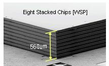
3 How Real is 3D??? 560μ Samsung 16Gb NAND flash (2Gx8 chips), Wide Bus DRAM Micron Wide Bus DRAM Intel CPU + memory OKI CMOS Sensor Xilinx 4 die 65nm interposer Raytheon/Ziptronix PIN Detector Device IBM RF Silicon Circuit Board / TSV Logic & Analog Toshiba 3D NAND 3


4 3D Stacking Approaches Chip Level Device Level Wafer Level Ziptronix Vertical Circuits Elpida/Micron/Samsung Amkor : 4S CSP (MCP) Stanford Besang Sandisk: Vertical TFT Infineon/IBM RPI ZyCube Tezzaron Irvine Sensors : Stacked Flash Samsung : Stacked Flash 4


5 Span of 3D Integration Packaging Analog Flash DRAM DRAM CPU 3D Through Via Chip Stack IBM/Samsung 3D-ICs 100-1,000,000/sqmm M Interconnects/device CMOS 3D Wafer Fab IBM 1s/sqmm Peripheral I/O Flash, DRAM CMOS Sensors 100,000,000s/sqmm Transistor to Transistor Ultimate goal 5
6 A Closer Look at Wafer-Level Stacking Oxide Silicon Dielectric(SiO2/SiN) Gate Poly STI (Shallow Trench Isolation) W (Tungsten contact & via) Al (M1 M5) Cu (M6, Top Metal) Super-Contact 6
7 Next, Stack a Second Wafer & Thin: 7


8 Stacking Process Sequential Picture Two wafer Align & Bond Course Grinded Fine Grinded High Precision Alignment Misalign=0.3um After CMP Si Recessed Top wafer Bottom wafer 8
9 Then, Stack a Third Wafer: 3rd wafer 2nd wafer 1st wafer: controller 9
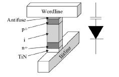
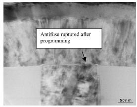
10 Finally, Flip, Thin & Pad Out: 1st wafer: controller 2nd wafer This is the completed stack! 3rd wafer 10


11 3 rd Si thinned to 5.5um 2 nd Si thinned to 5.5um SiO 2 1 st Si bottom supporting wafer 11
12 3D Interconnect Characteristics SuperContact TM SuperContact TM SuperContact TM SuperContact TM Bond Points I II III 4 200mm 300mm 200mm 200mm Via First, FEOL Via First, FEOL Via First, FEOL Via First, FEOL Size 1.2 X X X X X 1.7 L X W X D X 6.0 X 10.0 X 10 X 2 Cu Material W in Bulk W in Bulk W in Bulk W in SOI Minimum Pitch <2.5 < (1.1 Feedthrough Capacitance 2-3fF 6fF 3fF 0.2fF << Series Resistance <1.5 <1.8 <3 <1.5 < 12

13 Relative TSV Size 13
14 Pitch and Interconnect SuperContact TM is 500f 2 (including spacing) Face to face is 350f 2 (including spacing) Chip on wafer I/O pitch is 35,000f 2 Standard cell gate is 200 to 1000f 2 3 connections Standard cell flip-flop is 5000f 2 5 connections 16 bit sync-counter is 125,000f 2 20 connections Opamp is 300,000f 2 4 connections f 2 is minimum feature squared 14
15 R8051/Memory 5X Performance 1/10 th Power 15
16 16


17 New Apps New Architectures 17
18 Dis-Integrated 3D Memory Memory Layers Bitlines Memory Cells Wordlines Power,Ground, VBB,VDH Controller Layer Senseamps I/O Drivers Wordline Drivers 18
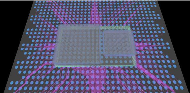
 <20ns full cycle memory time 288GB/s data transfer rate Max clk=1.")

19 Octopus DRAM 1-4Gb 16 Ports x 128bits (each CWL=0 CRL=2 SDR format 7ns closed page access to first data (aligned) <20ns full cycle memory time 288GB/s data transfer rate Max clk=1.6ghz Internally ECC protected, Dynamic self-repair, Post attach repair 115C die full function operating temperature JTAG/Mailbox test&configuration Power -40% Density x4++ Performance +300% Cost -50% 19

20 Octopus DRAM Layer 20

21 Octopus Controller 21


22 Main Memory Power Cliff DDR3 ~40mW per pin 1024 Data pins 40W 4096 Data pins 160W Die on Wafer ~24uW per pin 22
23 DDR2/3/4 Memory Channels The Industry Issue To continue to increase CPU performance, exponential bandwidth growth required Best Case Number of channels to support Float OPS Worst Case Number of channels to support Float OPS Best Case Number of channels to support OPS Worst Case Number of channels to support OPS Best Case Number of channels to support mixed OPS More than 200 CPU cycles of delay to memory results in cycle for cycle CPU stalls. 16 to 64 Mbytes per thread required to hide CPU memory system accesses. 1 Need 50x bandwidth improvement. Need 10x better cost model than embedded memory. No current extension of existing IC technology can address requirements. Memory I/O power is running away. 23


24 The Killer App: Split-Die Tezzaron 3D DRAM Embedded Performance with far superior cost/density. 110nm DRAM node has better density than 45nm embedded DRAM. 1000x reduction in I/O power. DRAM Customer Host Device I/O Pad area : Bumping or wire bonding 24
25 Die to Wafer With Stencils Diced Memory Stack CPU die Stencil Window 25


26 Die to Wafer With BCB Template RPI Effort under Dr. James Lu KGD 2um alignment / 5um pitch limit Cu-Cu thermo compression bonding Multilayer capability 26


27 Logic on Memory 172 pads 199 I/O Bondpoints/side Memory also acts as interposer 92 pads (528 total pads at edge, stagger 250um pad, 125um pitch ~1500 available pads) 8 DRAM ports 16x21 pad array >10 f bypass caps SS ~4,000pf 27
 Hyper-Integration Controller Memory Memory 5-9 layer stacks Bond pads 528 available Stagger 125um pitch TSVs Layer 5 Layer 7 Layer 9 Layer Poly 9")
28 2-4 layer logic device Face to Face Bond 5x5 mm Octopus memory device 21.8x12.3 mm (2-5 layer) Hyper-Integration Controller Memory Memory 5-9 layer stacks Bond pads 528 available Stagger 125um pitch TSVs Layer 5 Layer 7 Layer 9 Layer Poly Copper Wire 21 (25) 32 (38) 34 (42) Al/W Wire Trans. Count 3B 3.1B 5.5B 28
29 Tools Partitioning tools 3D P&R Access Testing IEEE 1500 IEEE 1149 Standards 3D Challenges Die level JEDEC JC-11 Wide bus memory Foundry interface 29


30 MAX-3D by Micro Magic, Inc. Fully functional 3D layout editor. Independent tech files for each tier. Saves GDSII as flipped or rotated. Custom output streams for 3D DRC / LVS. DRC, LVS, Transistor synthesis, Crossprobing. Multiple tapeouts, 0.35um-45nm >20GB, ~10B devices 30


31 3D LVS using QuartzLVS from Magma Key features LVS each of the 2D designs as well as the 3D interconnections between them in a single run Driven by a 3D tech file that specifies the number and order of layers, interconnect material, etc TSV aware LVS extraction Full debug environment to analyze any LVS mismatch # 3D LVS Tech file WAFER: 1 LAYOUT TOP BLOCK: lvslayer1_1 SCHEMATIC TOP BLOCK: lvslayer1 GDSII FILE: lvslayer1_1.gds SCHEMATIC NETLIST: lvslayer1.sp INTERFACE UP METAL: 1;0 INTERFACE UP TEXT: 1; INTERFACE: LAYOUT TOP BLOCK: lvstop SCHEMATIC TOP BLOCK: lvstop GDSII FILE: lvstop_all.gds SCHEMATIC NETLIST: lvstop.sp BOND OUT METAL: 5;0 BOND OUT TEXT: 5;101 31


32 R3Logic 3DIntegrator High level partitioning 3 rd Party R3Integrator 3 rd Party 32

33 3D MPW Complete 3D PDK 7 th Release GF 130nm Calibre, Synopsis, Hspice, Cadence MicroMagic 3D physical editor Magma 3D DRC/LVS Artisan standard cell libraries Release 8 up coming MOSIS, CMP, and CMC MPW support July 1 st MPW Tapeout 90nm, 150nm SOI Silicon Workbench >70 in process >400 users 33
34 Near End-of-Line M8 TM M7 M6 M5 M4 M4 M5 2x,4x,8x Wiring level ~.2/.2um S/W M3 SIN W M2 M1 poly STI TSV is 1.2µ Wide and ~10µ deep 5.6µ 34
35 OC768 Packet Engine How do we test this? Test Engines (BIST, BISR) & NOCs Dual PPC 64x ARM SOC FPGA (CPU Augmentation) DRAM Flash CAM CAM FPGA (Packet Cracker) Stack Controller 35
36 Power Control Timing Control UC Event Detection TAP 8051 core Test Core Test Core Memory Bank Memory Bank Test Core Memory Bank EDAC Test Core Memory Bank PROM Test Core Test Core Memory Bank Memory Bank ROM Test Core Memory Bank SRAM Test Core Memory Bank 36
37 Memory Test Processor 1 inst/clk At speed testing Register file with inc/dec and compare Row, Column, Layer Special complex instructions Activate, Test, Branch, Inc/Dec Data Scramble by Row, Column, Layer Restart instruction insertion Probe mode 37


38 Network-On-Chip: 3D-Routing Node UP WEST NORTH SOUTH EAST TBUS DOWN 38
39 Fault Tolerant Self-configuring/Re-configuring Stack Manager tbus Processor0 TBS TBU tbus TBC tbus routing nodes Stack Manager tbus Processor1 TBS TBU tbus TBC tbus routing nodes 39
40 3D Interconnect 40

41 Summary 3D has numerous and vast opportunities!! New design approaches New ways of thinking New tools Poised for explosive growth 1-3 generation shrink equivalent Sensors Computing MEMS Communications 41
3D Integration: New Opportunities for Speed, Power and Performance. Robert Patti, CTO
 3D Integration: New Opportunities for Speed, Power and Performance Robert Patti, CTO rpatti@tezzaron.com 1 Advantages Why We Scale? What can 3D do for us? Speed Power Cost Size >180nm 130nm 90nm 65nm 45nm
EECS 598: Integrating Emerging Technologies with Computer Architecture. Lecture 10: Three-Dimensional (3D) Integration
 Integration") 1 EECS 598: Integrating Emerging Technologies with Computer Architecture Lecture 10: Three-Dimensional (3D) Integration Instructor: Ron Dreslinski Winter 2016 University of Michigan 1 1 1 Announcements
1 EECS 598: Integrating Emerging Technologies with Computer Architecture Lecture 10: Three-Dimensional (3D) Integration Instructor: Ron Dreslinski Winter 2016 University of Michigan 1 1 1 Announcements
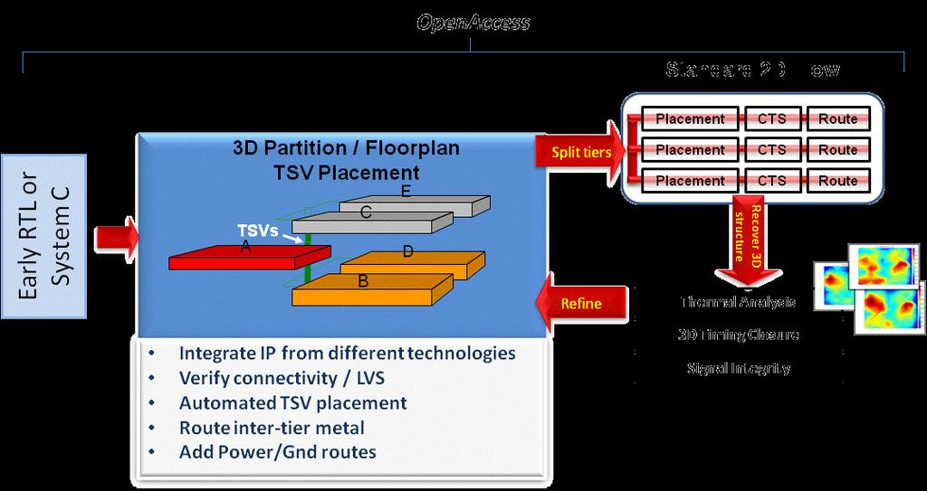
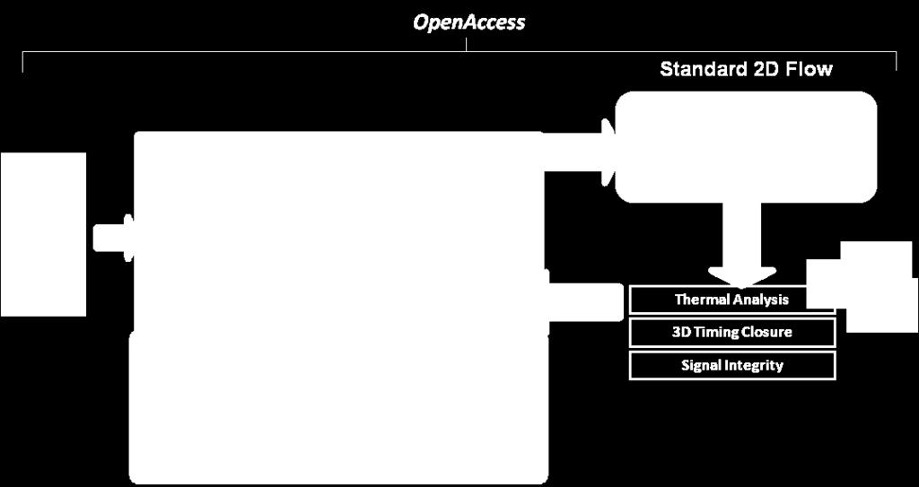
Physical Design Implementation for 3D IC Methodology and Tools. Dave Noice Vassilios Gerousis
 I NVENTIVE Physical Design Implementation for 3D IC Methodology and Tools Dave Noice Vassilios Gerousis Outline 3D IC Physical components Modeling 3D IC Stack Configuration Physical Design With TSV Summary
3D TECHNOLOGIES: SOME PERSPECTIVES FOR MEMORY INTERCONNECT AND CONTROLLER
 3D TECHNOLOGIES: SOME PERSPECTIVES FOR MEMORY INTERCONNECT AND CONTROLLER CODES+ISSS: Special session on memory controllers Taipei, October 10 th 2011 Denis Dutoit, Fabien Clermidy, Pascal Vivet {denis.dutoit@cea.fr}
Interconnect Challenges in a Many Core Compute Environment. Jerry Bautista, PhD Gen Mgr, New Business Initiatives Intel, Tech and Manuf Grp
 Interconnect Challenges in a Many Core Compute Environment Jerry Bautista, PhD Gen Mgr, New Business Initiatives Intel, Tech and Manuf Grp Agenda Microprocessor general trends Implications Tradeoffs Summary
Stacking Untested Wafers to Improve Yield. The 3D Enigma
 Stacking Untested Wafers to Improve Yield or 3D: Where the Timid Go to Die The 3D Enigma The Promise High Performance Low Power Improved Density More than Moore or at least as much as Moore The Reality
3D SYSTEM INTEGRATION TECHNOLOGY CHOICES AND CHALLENGE ERIC BEYNE, ANTONIO LA MANNA
 3D SYSTEM INTEGRATION TECHNOLOGY CHOICES AND CHALLENGE ERIC BEYNE, ANTONIO LA MANNA OUTLINE 3D Application Drivers and Roadmap 3D Stacked-IC Technology 3D System-on-Chip: Fine grain partitioning Conclusion
Bringing 3D Integration to Packaging Mainstream
 Bringing 3D Integration to Packaging Mainstream Enabling a Microelectronic World MEPTEC Nov 2012 Choon Lee Technology HQ, Amkor Highlighted TSV in Packaging TSMC reveals plan for 3DIC design based on silicon
TSV Test. Marc Loranger Director of Test Technologies Nov 11 th 2009, Seoul Korea
 TSV Test Marc Loranger Director of Test Technologies Nov 11 th 2009, Seoul Korea # Agenda TSV Test Issues Reliability and Burn-in High Frequency Test at Probe (HFTAP) TSV Probing Issues DFT Opportunities
From 3D Toolbox to 3D Integration: Examples of Successful 3D Applicative Demonstrators N.Sillon. CEA. All rights reserved
 From 3D Toolbox to 3D Integration: Examples of Successful 3D Applicative Demonstrators N.Sillon Agenda Introduction 2,5D: Silicon Interposer 3DIC: Wide I/O Memory-On-Logic 3D Packaging: X-Ray sensor Conclusion
Monolithic 3D Integration using Standard Fab & Standard Transistors. Zvi Or-Bach CEO MonolithIC 3D Inc.
 Monolithic 3D Integration using Standard Fab & Standard Transistors Zvi Or-Bach CEO MonolithIC 3D Inc. 3D Integration Through Silicon Via ( TSV ), Monolithic Increase integration Reduce interconnect total
Xilinx SSI Technology Concept to Silicon Development Overview
 Xilinx SSI Technology Concept to Silicon Development Overview Shankar Lakka Aug 27 th, 2012 Agenda Economic Drivers and Technical Challenges Xilinx SSI Technology, Power, Performance SSI Development Overview
Advancing high performance heterogeneous integration through die stacking
 Advancing high performance heterogeneous integration through die stacking Suresh Ramalingam Senior Director, Advanced Packaging European 3D TSV Summit Jan 22 23, 2013 The First Wave of 3D ICs Perfecting
edram to the Rescue Why edram 1/3 Area 1/5 Power SER 2-3 Fit/Mbit vs 2k-5k for SRAM Smaller is faster What s Next?
 edram to the Rescue Why edram 1/3 Area 1/5 Power SER 2-3 Fit/Mbit vs 2k-5k for SRAM Smaller is faster What s Next? 1 Integrating DRAM and Logic Integrate with Logic without impacting logic Performance,
DFT-3D: What it means to Design For 3DIC Test? Sanjiv Taneja Vice President, R&D Silicon Realization Group
 I N V E N T I V E DFT-3D: What it means to Design For 3DIC Test? Sanjiv Taneja Vice President, R&D Silicon Realization Group Moore s Law & More : Tall And Thin More than Moore: Diversification Moore s
Emerging IC Packaging Platforms for ICT Systems - MEPTEC, IMAPS and SEMI Bay Area Luncheon Presentation
 Emerging IC Packaging Platforms for ICT Systems - MEPTEC, IMAPS and SEMI Bay Area Luncheon Presentation Dr. Li Li Distinguished Engineer June 28, 2016 Outline Evolution of Internet The Promise of Internet
3D systems-on-chip. A clever partitioning of circuits to improve area, cost, power and performance. The 3D technology landscape
 Edition April 2017 Semiconductor technology & processing 3D systems-on-chip A clever partitioning of circuits to improve area, cost, power and performance. In recent years, the technology of 3D integration
Burn-in & Test Socket Workshop
 Burn-in & Test Socket Workshop IEEE March 4-7, 2001 Hilton Mesa Pavilion Hotel Mesa, Arizona IEEE COMPUTER SOCIETY Sponsored By The IEEE Computer Society Test Technology Technical Council COPYRIGHT NOTICE
A Design Tradeoff Study with Monolithic 3D Integration
 A Design Tradeoff Study with Monolithic 3D Integration Chang Liu and Sung Kyu Lim Georgia Institute of Techonology Atlanta, Georgia, 3332 Phone: (44) 894-315, Fax: (44) 385-1746 Abstract This paper studies
The Memory Hierarchy 1
 The Memory Hierarchy 1 What is a cache? 2 What problem do caches solve? 3 Memory CPU Abstraction: Big array of bytes Memory memory 4 Performance vs 1980 Processor vs Memory Performance Memory is very slow
PicoServer : Using 3D Stacking Technology To Enable A Compact Energy Efficient Chip Multiprocessor
 PicoServer : Using 3D Stacking Technology To Enable A Compact Energy Efficient Chip Multiprocessor Taeho Kgil, Shaun D Souza, Ali Saidi, Nathan Binkert, Ronald Dreslinski, Steve Reinhardt, Krisztian Flautner,
3D Integration & Packaging Challenges with through-silicon-vias (TSV)
") NSF Workshop 2/02/2012 3D Integration & Packaging Challenges with through-silicon-vias (TSV) Dr John U. Knickerbocker IBM - T.J. Watson Research, New York, USA Substrate IBM Research Acknowledgements IBM
NSF Workshop 2/02/2012 3D Integration & Packaging Challenges with through-silicon-vias (TSV) Dr John U. Knickerbocker IBM - T.J. Watson Research, New York, USA Substrate IBM Research Acknowledgements IBM
Design Methodologies and Tools. Full-Custom Design
 Design Methodologies and Tools Design styles Full-custom design Standard-cell design Programmable logic Gate arrays and field-programmable gate arrays (FPGAs) Sea of gates System-on-a-chip (embedded cores)
Wafer Level Packaging The Promise Evolves Dr. Thomas Di Stefano Centipede Systems, Inc. IWLPC 2008
 Wafer Level Packaging The Promise Evolves Dr. Thomas Di Stefano Centipede Systems, Inc. IWLPC 2008 / DEVICE 1.E+03 1.E+02 1.E+01 1.E+00 1.E-01 1.E-02 1.E-03 1.E-04 1.E-05 1.E-06 1.E-07 Productivity Gains
Vertical Circuits. Small Footprint Stacked Die Package and HVM Supply Chain Readiness. November 10, Marc Robinson Vertical Circuits, Inc
 Small Footprint Stacked Die Package and HVM Supply Chain Readiness Marc Robinson Vertical Circuits, Inc November 10, 2011 Vertical Circuits Building Blocks for 3D Interconnects Infrastructure Readiness
High Volume Manufacturing Supply Chain Ecosystem for 2.5D HBM2 ASIC SiPs
 Open-Silicon.com 490 N. McCarthy Blvd, #220 Milpitas, CA 95035 408-240-5700 HQ High Volume Manufacturing Supply Chain Ecosystem for 2.5D HBM2 ASIC SiPs Open-Silicon Asim Salim VP Mfg. Operations 20+ experience
Thermal Analysis on Face-to-Face(F2F)-bonded 3D ICs
-bonded 3D ICs") 1/16 Thermal Analysis on Face-to-Face(F2F)-bonded 3D ICs Kyungwook Chang, Sung-Kyu Lim School of Electrical and Computer Engineering Georgia Institute of Technology Introduction Challenges in 2D Device
1/16 Thermal Analysis on Face-to-Face(F2F)-bonded 3D ICs Kyungwook Chang, Sung-Kyu Lim School of Electrical and Computer Engineering Georgia Institute of Technology Introduction Challenges in 2D Device
Design Solutions in Foundry Environment. by Michael Rubin Agilent Technologies
 Design Solutions in Foundry Environment by Michael Rubin Agilent Technologies Presenter: Michael Rubin RFIC Engineer, R&D, Agilent Technologies former EDA Engineering Manager Agilent assignee at Chartered
An Overview of Standard Cell Based Digital VLSI Design
 An Overview of Standard Cell Based Digital VLSI Design With examples taken from the implementation of the 36-core AsAP1 chip and the 1000-core KiloCore chip Zhiyi Yu, Tinoosh Mohsenin, Aaron Stillmaker,
Near-Threshold Computing: Reclaiming Moore s Law
 1 Near-Threshold Computing: Reclaiming Moore s Law Dr. Ronald G. Dreslinski Research Fellow Ann Arbor 1 1 Motivation 1000000 Transistors (100,000's) 100000 10000 Power (W) Performance (GOPS) Efficiency (GOPS/W)
AIM Photonics: Manufacturing Challenges for Photonic Integrated Circuits
 AIM Photonics: Manufacturing Challenges for Photonic Integrated Circuits November 16, 2017 Michael Liehr Industry Driving Force EXA FLOP SCALE SYSTEM Blades SiPh Interconnect Network Memory Stack HP HyperX
CircuitsMulti-Projets
 From layout to chips CircuitsMulti-Projets MPW Services Center for ICs, Photonics & MEMS Prototyping & Low Volume Production mycmp.fr Grenoble - France From layout to chips STMicroelectronics Standard
The Design of the KiloCore Chip
 The Design of the KiloCore Chip Aaron Stillmaker*, Brent Bohnenstiehl, Bevan Baas DAC 2017: Design Challenges of New Processor Architectures University of California, Davis VLSI Computation Laboratory
Moore s s Law, 40 years and Counting
 Moore s s Law, 40 years and Counting Future Directions of Silicon and Packaging Bill Holt General Manager Technology and Manufacturing Group Intel Corporation InterPACK 05 2005 Heat Transfer Conference
Circuits Multi Projets
 Circuits Multi Projets MPW Services Center for IC / MEMS Prototyping http://cmp.imag.fr Grenoble France CMP annual users meeting, 4 Feb. 2016, PARIS STMicroelectronics Standard Technology offers at CMP
FABRICATION TECHNOLOGIES
 FABRICATION TECHNOLOGIES DSP Processor Design Approaches Full custom Standard cell** higher performance lower energy (power) lower per-part cost Gate array* FPGA* Programmable DSP Programmable general
Multi-Die Packaging How Ready Are We?
 Multi-Die Packaging How Ready Are We? Rich Rice ASE Group April 23 rd, 2015 Agenda ASE Brief Integration Drivers Multi-Chip Packaging 2.5D / 3D / SiP / SiM Design / Co-Design Challenges: an OSAT Perspective
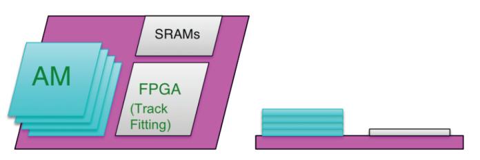
AMchip architecture & design
 Sezione di Milano AMchip architecture & design Alberto Stabile - INFN Milano AMchip theoretical principle Associative Memory chip: AMchip Dedicated VLSI device - maximum parallelism Each pattern with private
Design Methodologies. Full-Custom Design
 Design Methodologies Design styles Full-custom design Standard-cell design Programmable logic Gate arrays and field-programmable gate arrays (FPGAs) Sea of gates System-on-a-chip (embedded cores) Design
Introduction 1. GENERAL TRENDS. 1. The technology scale down DEEP SUBMICRON CMOS DESIGN
 1 Introduction The evolution of integrated circuit (IC) fabrication techniques is a unique fact in the history of modern industry. The improvements in terms of speed, density and cost have kept constant
WLSI Extends Si Processing and Supports Moore s Law. Douglas Yu TSMC R&D,
 WLSI Extends Si Processing and Supports Moore s Law Douglas Yu TSMC R&D, chyu@tsmc.com SiP Summit, Semicon Taiwan, Taipei, Taiwan, Sep. 9 th, 2016 Introduction Moore s Law Challenges Heterogeneous Integration
TechSearch International, Inc.
 Alternatives on the Road to 3D TSV E. Jan Vardaman President TechSearch International, Inc. www.techsearchinc.com Everyone Wants to Have 3D ICs 3D IC solves interconnect delay problem bandwidth bottleneck
High performance HBM Known Good Stack Testing
 High performance HBM Known Good Stack Testing FormFactor Teradyne Overview High Bandwidth Memory (HBM) Market and Technology Probing challenges Probe solution Power distribution challenges PDN design Simulation
Pushing the Boundaries of Moore's Law to Transition from FPGA to All Programmable Platform Ivo Bolsens, SVP & CTO Xilinx ISPD, March 2017
 Pushing the Boundaries of Moore's Law to Transition from FPGA to All Programmable Platform Ivo Bolsens, SVP & CTO Xilinx ISPD, March 2017 High Growth Markets Cloud Computing Automotive IIoT 5G Wireless
Comparison & highlight on the last 3D TSV technologies trends Romain Fraux
 Comparison & highlight on the last 3D TSV technologies trends Romain Fraux Advanced Packaging & MEMS Project Manager European 3D Summit 18 20 January, 2016 Outline About System Plus Consulting 2015 3D
Advanced Packaging For Mobile and Growth Products
 Advanced Packaging For Mobile and Growth Products Steve Anderson, Senior Director Product and Technology Marketing, STATS ChipPAC Growing Needs for Silicon & Package Integration Packaging Trend Implication
HEAT (Hardware enabled Algorithmic tester) for 2.5D HBM Solution
 for 2.5D HBM Solution") HEAT (Hardware enabled Algorithmic tester) for 2.5D HBM Solution Kunal Varshney, Open-Silicon Ganesh Venkatkrishnan, Open-Silicon Pankaj Prajapati, Open-Silicon May 9, 9, 2016 1 Agenda High Bandwidth Memory
HEAT (Hardware enabled Algorithmic tester) for 2.5D HBM Solution Kunal Varshney, Open-Silicon Ganesh Venkatkrishnan, Open-Silicon Pankaj Prajapati, Open-Silicon May 9, 9, 2016 1 Agenda High Bandwidth Memory
3D-IC is Now Real: Wide-IO is Driving 3D-IC TSV. Samta Bansal and Marc Greenberg, Cadence EDPS Monterey, CA April 5-6, 2012
 3D-IC is Now Real: Wide-IO is Driving 3D-IC TSV Samta Bansal and Marc Greenberg, Cadence EDPS Monterey, CA April 5-6, 2012 What the fuss is all about * Source : ECN Magazine March 2011 * Source : EDN Magazine
Calibrating Achievable Design GSRC Annual Review June 9, 2002
 Calibrating Achievable Design GSRC Annual Review June 9, 2002 Wayne Dai, Andrew Kahng, Tsu-Jae King, Wojciech Maly,, Igor Markov, Herman Schmit, Dennis Sylvester DUSD(Labs) Calibrating Achievable Design
The Processor That Don't Cost a Thing
 The Processor That Don't Cost a Thing Peter Hsu, Ph.D. Peter Hsu Consulting, Inc. http://cs.wisc.edu/~peterhsu DRAM+Processor Commercial demand Heat stiffling industry's growth Heat density limits small
Advanced Information Storage 11
 Advanced Information Storage 11 Atsufumi Hirohata Department of Electronics 16:00 11/November/2013 Monday (P/L 002) Quick Review over the Last Lecture Shingled write recording : * Bit patterned media (BPM)
Chapter 0 Introduction
 Chapter 0 Introduction Jin-Fu Li Laboratory Department of Electrical Engineering National Central University Jhongli, Taiwan Applications of ICs Consumer Electronics Automotive Electronics Green Power
ASIC Physical Design Top-Level Chip Layout
 ASIC Physical Design Top-Level Chip Layout References: M. Smith, Application Specific Integrated Circuits, Chap. 16 Cadence Virtuoso User Manual Top-level IC design process Typically done before individual
Non-contact Test at Advanced Process Nodes
 Chris Sellathamby, J. Hintzke, B. Moore, S. Slupsky Scanimetrics Inc. Non-contact Test at Advanced Process Nodes June 8-11, 8 2008 San Diego, CA USA Overview Advanced CMOS nodes are a challenge for wafer
Photonics Integration in Si P Platform May 27 th Fiber to the Chip
 Photonics Integration in Si P Platform May 27 th 2014 Fiber to the Chip Overview Introduction & Goal of Silicon Photonics Silicon Photonics Technology Wafer Level Optical Test Integration with Electronics
IMEC CORE CMOS P. MARCHAL
 APPLICATIONS & 3D TECHNOLOGY IMEC CORE CMOS P. MARCHAL OUTLINE What is important to spec 3D technology How to set specs for the different applications - Mobile consumer - Memory - High performance Conclusions
KiloCore: A 32 nm 1000-Processor Array
 KiloCore: A 32 nm 1000-Processor Array Brent Bohnenstiehl, Aaron Stillmaker, Jon Pimentel, Timothy Andreas, Bin Liu, Anh Tran, Emmanuel Adeagbo, Bevan Baas University of California, Davis VLSI Computation
Future Memories. Jim Handy OBJECTIVE ANALYSIS
 Future Memories Jim Handy OBJECTIVE ANALYSIS Hitting a Brick Wall OBJECTIVE ANALYSIS www.objective-analysis.com Panelists Michael Miller VP Technology, Innovation & Systems Applications MoSys Christophe
ARCHIVE Françoise von Trapp Editorial Director 3D InCites ABSTRACT
 2010 Invited Speaker ARCHIVE 2010 RISING TO THE 3D TSV TEST CHALLENGE: WILL YOU BE READY? by Françoise von Trapp Editorial Director 3D InCites 3D ABSTRACT integration is not a novel concept. Veterans in
L évolution des architectures et des technologies d intégration des circuits intégrés dans les Data centers
 I N S T I T U T D E R E C H E R C H E T E C H N O L O G I Q U E L évolution des architectures et des technologies d intégration des circuits intégrés dans les Data centers 10/04/2017 Les Rendez-vous de
Interposer Technology: Past, Now, and Future
 Interposer Technology: Past, Now, and Future Shang Y. Hou TSMC 侯上勇 3D TSV: Have We Waited Long Enough? Garrou (2014): A Little More Patience Required for 2.5/3D All things come to those who wait In 2016,
ESE 570 Cadence Lab Assignment 2: Introduction to Spectre, Manual Layout Drawing and Post Layout Simulation (PLS)
") ESE 570 Cadence Lab Assignment 2: Introduction to Spectre, Manual Layout Drawing and Post Layout Simulation (PLS) Objective Part A: To become acquainted with Spectre (or HSpice) by simulating an inverter,
ESE 570 Cadence Lab Assignment 2: Introduction to Spectre, Manual Layout Drawing and Post Layout Simulation (PLS) Objective Part A: To become acquainted with Spectre (or HSpice) by simulating an inverter,
UCLA 3D research started in 2002 under DARPA with CFDRC
 Coping with Vertical Interconnect Bottleneck Jason Cong UCLA Computer Science Department cong@cs.ucla.edu http://cadlab.cs.ucla.edu/ cs edu/~cong Outline Lessons learned Research challenges and opportunities
Spiral 2-8. Cell Layout
 2-8.1 Spiral 2-8 Cell Layout 2-8.2 Learning Outcomes I understand how a digital circuit is composed of layers of materials forming transistors and wires I understand how each layer is expressed as geometric
Paul Franzon. Department of Electrical and Computer Engineering
 Architectures for Extremely Scaled Memories Paul Franzon Department of Electrical and Computer Engineering paulf@ncsu.edu 919.515.7351 High Level Overview Challenges for Memories Bandwidth Power consumption
Current status of SOI / MPU and ASIC development for space
 The 23rd Microelectronics Workshop Current status of SOI / MPU and ASIC development for space Nov. 11 th 2010 Electronic Devices and Materials Group Aerospace Research and Development Directorate, JAXA
Additional Slides for Lecture 17. EE 271 Lecture 17
 Additional Slides for Lecture 17 Advantages/Disadvantages of Wire Bonding Pros Cost: cheapest packages use wire bonding Allows ready access to front side of die for probing Cons Relatively high inductance
WaferBoard Rapid Prototyping
 WaferBoard Rapid Prototyping WaferBoard (cover not shown) 1. Select components that are packaged in ball grid array, QFP, TSOP, etc. 2. Place the packaged components FPGAs, ASICs, processors, memories,
TechSearch International, Inc.
 On the Road to 3D ICs: Markets and Solutions E. Jan Vardaman President TechSearch International, Inc. www.techsearchinc.com High future cost of lithography Severe interconnect delay Noted in ITRS roadmap
Memory in Digital Systems
 MEMORIES Memory in Digital Systems Three primary components of digital systems Datapath (does the work) Control (manager) Memory (storage) Single bit ( foround ) Clockless latches e.g., SR latch Clocked
The communication bottleneck
 3D-MPSoCs: architectural and design technology outlook Luca Benini DEIS Università di Bologna lbenini@deis.unibo.it The communication bottleneck Architectural issues Traditional shared buses do not scale
technology Leadership
 technology Leadership MARK BOHR INTEL SENIOR FELLOW, TECHNOLOGY AND MANUFACTURING GROUP DIRECTOR, PROCESS ARCHITECTURE AND INTEGRATION SEPTEMBER 19, 2017 Legal Disclaimer DISCLOSURES China Tech and Manufacturing
Power dissipation! The VLSI Interconnect Challenge. Interconnect is the crux of the problem. Interconnect is the crux of the problem.
 The VLSI Interconnect Challenge Avinoam Kolodny Electrical Engineering Department Technion Israel Institute of Technology VLSI Challenges System complexity Performance Tolerance to digital noise and faults
On GPU Bus Power Reduction with 3D IC Technologies
 On GPU Bus Power Reduction with 3D Technologies Young-Joon Lee and Sung Kyu Lim School of ECE, Georgia Institute of Technology, Atlanta, Georgia, USA yjlee@gatech.edu, limsk@ece.gatech.edu Abstract The
The Foundry-Packaging Partnership. Enabling Future Performance. Jon A. Casey. IBM Systems and Technology Group
 The Foundry-Packaging Partnership Enabling Future Performance Jon A. Casey IBM Fellow IBM Systems and Technology Group 5/30/2013 2012 IBM Corporation Data growth will drive the new IT model Dimensions
All Programmable: from Silicon to System
 All Programmable: from Silicon to System Ivo Bolsens, Senior Vice President & CTO Page 1 Moore s Law: The Technology Pipeline Page 2 Industry Debates Variability Page 3 Industry Debates on Cost Page 4
DFT Trends in the More than Moore Era. Stephen Pateras Mentor Graphics
 DFT Trends in the More than Moore Era Stephen Pateras Mentor Graphics steve_pateras@mentor.com Silicon Valley Test Conference 2011 1 Outline Semiconductor Technology Trends DFT in relation to: Increasing
Chip/Package/Board Design Flow
 Chip/Package/Board Design Flow EM Simulation Advances in ADS 2011.10 1 EM Simulation Advances in ADS2011.10 Agilent EEsof Chip/Package/Board Design Flow 2 RF Chip/Package/Board Design Industry Trends Increasing
On the Design of Ultra-High Density 14nm Finfet based Transistor-Level Monolithic 3D ICs
 2016 IEEE Computer Society Annual Symposium on VLSI On the Design of Ultra-High Density 14nm Finfet based Transistor-Level Monolithic 3D ICs Jiajun Shi 1,2, Deepak Nayak 1,Motoi Ichihashi 1, Srinivasa
Chapter 5: ASICs Vs. PLDs
 Chapter 5: ASICs Vs. PLDs 5.1 Introduction A general definition of the term Application Specific Integrated Circuit (ASIC) is virtually every type of chip that is designed to perform a dedicated task.
Gigascale Integration Design Challenges & Opportunities. Shekhar Borkar Circuit Research, Intel Labs October 24, 2004
 Gigascale Integration Design Challenges & Opportunities Shekhar Borkar Circuit Research, Intel Labs October 24, 2004 Outline CMOS technology challenges Technology, circuit and μarchitecture solutions Integration
Chapter 2 Three-Dimensional Integration: A More Than Moore Technology
 Chapter 2 Three-Dimensional Integration: A More Than Moore Technology Abstract Three-dimensional integrated circuits (3D-ICs), which contain multiple layers of active devices, have the potential to dramatically
3-Dimensional (3D) ICs: A Survey
 ICs: A Survey") 3-Dimensional (3D) ICs: A Survey Lavanyashree B.J M.Tech, Student VLSI DESIGN AND EMBEDDED SYSTEMS Dayananda Sagar College of engineering, Bangalore. Abstract VLSI circuits are scaled to meet improved
3-Dimensional (3D) ICs: A Survey Lavanyashree B.J M.Tech, Student VLSI DESIGN AND EMBEDDED SYSTEMS Dayananda Sagar College of engineering, Bangalore. Abstract VLSI circuits are scaled to meet improved
Keynote Speaker. Matt Nowak Senior Director Advanced Technology Qualcomm CDMA Technologies
 Keynote Speaker Emerging High Density 3D Through Silicon Stacking (TSS) What s Next? Matt Nowak Senior Director Advanced Technology Qualcomm CDMA Technologies 8 Emerging High Density 3D Through Silicon
TSBCD025 High Voltage 0.25 mm BCDMOS
 TSBCD025 High Voltage 0.25 mm BCDMOS TSI Semiconductors' 0.25 mm process is a feature rich platform with best in class CMOS, LDMOS, and BiPolar devices. The BCD technology enables logic, Mixed-Signal,
Paradigms Shifts in CMP
 Paradigms Shifts in CMP Daniel Redfield Director - NMA CMPUG - Semicon West 2018 Paradigm Shifts in CMP State of CMP Market Inflections are driving CMP Growth and Complexity Paradigm Shifts in CMP Strategies
Technologies and Tools for µe design
 Technologies and Tools for µe design What can CERN offer -PH-ESE Outline Technologies and Tools Status ASIC Testing infrastructure Packaging common needs 2 1 - ASIC Technologies CMOS 130 and 90 nm RF technologies,
Technology Platform Segmentation
 HOW TECHNOLOGY R&D LEADERSHIP BRINGS A COMPETITIVE ADVANTAGE FOR MULTIMEDIA CONVERGENCE Technology Platform Segmentation HP LP 2 1 Technology Platform KPIs Performance Design simplicity Power leakage Cost
Japanese two Samurai semiconductor ventures succeeded in near 3D-IC but failed the business, why? and what's left?
 Japanese two Samurai semiconductor ventures succeeded in near 3D-IC but failed the business, why? and what's left? Liquid Design Systems, Inc CEO Naoya Tohyama Overview of this presentation Those slides
3D Technologies For Low Power Integrated Circuits
 3D Technologies For Low Power Integrated Circuits Paul Franzon North Carolina State University Raleigh, NC paulf@ncsu.edu 919.515.7351 Outline 3DIC Technology Set Approaches to 3D Specific Power Minimization
Embedded Memory Alternatives
 EE241 - Spring 2005 Advanced Digital Integrated Circuits Lecture 26: Embedded Memory - Flash Slides Courtesy of Randy McKee, TI Embedded Memory Alternatives Courtesy Randy McKee, TI 2 1 3 4 2 5 SRAM 3
Z-RAM Ultra-Dense Memory for 90nm and Below. Hot Chips David E. Fisch, Anant Singh, Greg Popov Innovative Silicon Inc.
 Z-RAM Ultra-Dense Memory for 90nm and Below Hot Chips 2006 David E. Fisch, Anant Singh, Greg Popov Innovative Silicon Inc. Outline Device Overview Operation Architecture Features Challenges Z-RAM Performance
Stacked Silicon Interconnect Technology (SSIT)
") Stacked Silicon Interconnect Technology (SSIT) Suresh Ramalingam Xilinx Inc. MEPTEC, January 12, 2011 Agenda Background and Motivation Stacked Silicon Interconnect Technology Summary Background and Motivation
Stacked Silicon Interconnect Technology (SSIT) Suresh Ramalingam Xilinx Inc. MEPTEC, January 12, 2011 Agenda Background and Motivation Stacked Silicon Interconnect Technology Summary Background and Motivation
Centip3De: A 64-Core, 3D Stacked, Near-Threshold System
 1 1 1 Centip3De: A 64-Core, 3D Stacked, Near-Threshold System Ronald G. Dreslinski David Fick, Bharan Giridhar, Gyouho Kim, Sangwon Seo, Matthew Fojtik, Sudhir Satpathy, Yoonmyung Lee, Daeyeon Kim, Nurrachman
ENEE 759H, Spring 2005 Memory Systems: Architecture and
 SLIDE, Memory Systems: DRAM Device Circuits and Architecture Credit where credit is due: Slides contain original artwork ( Jacob, Wang 005) Overview Processor Processor System Controller Memory Controller
Design Methodologies
 Design Methodologies 1981 1983 1985 1987 1989 1991 1993 1995 1997 1999 2001 2003 2005 2007 2009 Complexity Productivity (K) Trans./Staff - Mo. Productivity Trends Logic Transistor per Chip (M) 10,000 0.1
Soitec ultra-thin SOI substrates enabling FD-SOI technology. July, 2015
 Soitec ultra-thin SOI substrates enabling FD-SOI technology July, 2015 Agenda FD-SOI: Background & Value Proposition C1- Restricted July 8, 2015 2 Today Ultra-mobile & Connected Consumer At Any Time With
Advanced Heterogeneous Solutions for System Integration
 Advanced Heterogeneous Solutions for System Integration Kees Joosse Director Sales, Israel TSMC High-Growth Applications Drive Product and Technology Smartphone Cloud Data Center IoT CAGR 12 17 20% 24%
MEMORIES. Memories. EEC 116, B. Baas 3
 MEMORIES Memories VLSI memories can be classified as belonging to one of two major categories: Individual registers, single bit, or foreground memories Clocked: Transparent latches and Flip-flops Unclocked:
Industry Trends in 3D and Advanced Packaging
 Industry Trends in 3D and Advanced Packaging Outline Industry System and Component Challenges & Trends 3D and Advanced Packaging Value-proposition and Client Examples 3D Technology Details 3DIC / 3DTSV