8051 MICROCONTROLLER
|
|
|
- Harriet Grant
- 6 years ago
- Views:
Transcription

1 What is a Microcontroller? UNIT MICROCONTROLLER A Microcontroller is a programmable digital processor with necessary peripherals. Both microcontrollers and microprocessors are complex sequential digital circuits meant to carry out job according to the program / instructions. Sometimes analog input/output interface makes a part of microcontroller circuit of mixed mode (both analog and digital nature). A microcontroller can be compared to a Swiss knife with multiple functions incorporated in the same IC. Fig. 5.1 A Microcontroller compared with a Swiss knife Microcontrollers Vs Microprocessors 1. A microprocessor requires an external memory for program/data storage. Instruction execution requires movement of data from the external memory to the microprocessor or vice versa. Usually, microprocessors have good computing power and they have higher clock speed to facilitate faster computation. 2. A microcontroller has required on-chip memory with associated peripherals. A microcontroller can be thought of a microprocessor with inbuilt peripherals. 3. A microcontroller does not require much additional interfacing ICs for operation and it functions as a standalone system. The operation of a microcontroller is multipurpose, just like a Swiss knife. 4. Microcontrollers are also called embedded controllers. A microcontroller clock speed is limited only
2 to a few tens of MHz Microcontrollers are numerous and many of them are application specific. Development/Classification of microcontrollers (Invisible) Microcontrollers have gone through a silent evolution (invisible). The evolution can be rightly termed as silent as the impact or application of a microcontroller is not well known to a common user, although microcontroller technology has undergone significant change since early 1970's. Development of some popular microcontrollers is given as follows. Intel bit (2300 PMOS trans, 108 khz) 1971 Intel bit 1976 Intel bit (ROM-less). Intel bit (Mask ROM) 1980 Microchip PIC16C64 8 bit 1985 Motorola 68HC11 8 bit (on chip ADC). Intel 80C bit 1982 Atmel AT89C51 8 bit (Flash memory). Microchip PIC 16F877 8 bit (Flash memory + ADC). Development of microprocessors (Visible) Microprocessors have undergone significant evolution over the past four decades. This development is clearly perceptible to a common user, especially, in terms of phenomenal growth in capabilities of personal computers. Development of some of the microprocessors can be given as follows. Intel bit (2300 PMOS transistors) 1971 Intel Intel Intel bit (NMOS) 8 bit 16 bit 16 bit 16 bit 16 bit
3 Intel bit ( transistors) 1985 Intel SX DX 32 bit 32 bit (built in floating point unit) 1989 Intel I MMX Celeron II III IV 64 bit Z-80 (Zilog) 8 bit 1976 Motorola Power PC bit Some of the microcontrollers of 8051 family are given as follows: DEVICE ON-CHIP DATA MEMORY (bytes) ON-CHIP PROGRAM MEMORY (bytes) 16-BIT TIMER/COUNTER NO. OF VECTORED INTERUPTS FULL DUPLEX I/O None none k ROM k ROM k EPROM k EPROM AT89C k Flash Memory AT89C k Flash memory 3 6 1
4 Various features of 8051 microcontroller are given as follows: 8-bit CPU 16-bit Program Counter 8-bit Processor Status Word (PSW) 8-bit Stack Pointer Internal RAM of 128bytes Special Function Registers (SFRs) of 128 bytes 32 I/O pins arranged as four 8-bit ports (P0 - P3) Two 16-bit timer/counters : T0 and T1 Two external and three internal vectored interrupts One full duplex serial I/O ARCHITECTURE OF 8051 MICROCONTROLLER: It is 8-bit microcontroller, means MC 8051 can Read, Write and Process 8 bit data. This is mostly used microcontroller in the robotics, home appliances like mp3 player, washing machines, electronic iron and industries. Mostly used blocks in the architecture of 8051 are as follows:

5 1. Oscillator and clock generator: All operations in a microcontroller are synchronized by the help of an oscillator clock. The oscillator clock generates the clock pulses by which all internal operations are synchronized. A resonant network connected through pins XTAL1 and XTAL2 forms up an oscillator. For this purpose a quartz crystal and capacitors are employed. The crystal run at specified maximum and minimum frequencies typically at 1 MHz to 16 MHz.
6 2. ALU: It is 8 bit unit. It performs arithmetic operation as addition, subtraction, multiplication, division, increment and decrement. It performs logical operations like AND, OR and EX-OR. It manipulates 8 bit and 16 bit data. It calculates address of jump locations in relative branch instruction. It performs compare, rotate and compliment operations. It consists of Boolean processor which performs bit, set, test, clear and compliment micro controller contains 34 general purpose registers or working registers.2 of them are called math registers A & B and 32 are bank of registers. a. Accumulator(A-reg): It is 8 bit register. Its address is E0H and it is bit and byte accessible. Result of arithmetic & logic operations performed by ALU is accumulated by this register. Therefore it is called accumulator register. It is used to store 8 bit data and to hold one of operand of ALU units during arithmetical and logical operations. Most of the instructions are carried out on accumulator data. It is most versatile of 2 CPU registers. b. B-register: It is special 8 bit math register. It is bit and byte accessible. It is used in conjunction with A register as I/P operand for ALU. It is used as general purpose register to store 8 bit data. c. PSW: It is 8 bit register. Its address is D0H and It is bit and byte accessible. It has 4 conditional flags or math flags which sets or resets according to condition of result. It has 3 control flags, by setting or resetting bit required operation or function can be achieved. The format of flag register is as shown below: d. FLAG: 1. Carry Flag(CY): During addition and subtraction any carry or borrow is generated then carry flag is set otherwise carry flag resets. It is used in arithmetic, logical, jump, rotate and Boolean operations. 2. Auxiliary carry flag(ac): If during addition and subtraction any carry or borrow is generated from lower 4 bit to higher 4 bit then AC sets else it resets. It is used in BCD arithmetic operations. 3. Overflow flag(ov): If in signed arithmetic operations result exceeds more than 7 bit than OV flag sets else resets.it is used in signed arithmetic operations only. 4. Parity flag(p): If in result, even no. Of ones "1" are present than it is called even parity and parity flag sets. In result odd no. Of ones "1"are present than it is called odd parity and parity flag resets. ii. CONTROL FLAGS: 1. FO: It is user defined flag. The user defines the function of this flag. The user can set,test n clear this flag through software. 2. RS1 and RS0: These flags are used to select bank of register by resetting those flags which are as shown in table :
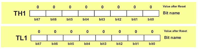
7 3. Program counter (PC): The Program Counter (PC) is a 2-byte address which tells the 8051 where the next instruction to execute is found in memory. It is used to hold 16 bit address of internal RAM, external RAM or external ROM locations. When the 8051 is initialized PC always starts at 0000h and is incremented each time an instruction is executed. It is important to note that PC isnt always incremented by one and never decremented. 4. Data pointer register (DTPR): It is a 16 bit register used to hold address of external or internal RAM where data is stored or result is to be stored. It is used to store 16 bit data. It is divided into2-8bit registers, DPH-data pointer higher order (83H) and DPL-data pointer lower order (82H). Each register can be used as general purpose register to store 8 bit data and can also be used as memory location. DPTR does not have single internal address. It functions as Base register in base relative addressing mode and in-direct jump. 5. Stack pointer (SP): It is 8-bit register. It is byte addressable. Its address is 81H. It is used to hold the internal RAM memory location addresses which are used as stack memory. When the data is to be placed on stack by push instruction, the content of stack pointer is incremented by 1, and when data is retrieved from stack, content of stack of stack pointer is decremented by 1. iii. Special function Registers(SFR): The 8051 microcontroller has 11 SFR divided in 4 groups: A. Timer/Counter register: 8051 microcontroller has 2-16 bit Timer/counter registers called Timer-reg-T0 And Timer/counter Reg-T1.Each register is 16 bit register divide into lower and higher byte register as shown below: These register are used to hold initial no. of count. All of the 4 register are byte addressable. 1. Timer control register: 8051 microcontroller has two 8-bit timer control register i.e. TMOD and TCON register. TMOD Register: it is 8-bit register. Its address is 89H. It is byte addressable. It used to select mode and control operation of time by writing control word. 2. TCON register: It is 8-bit register. Its address is 88H. It is byte addressable. Its MSB 4- bit are used to control operation of timer/ counter and LSB 4-bit are used for external interrupt control. B. Serial data register: 8051 micro controller has 2 serial data register viz. SBUF and SCON. 1. Serial buffer register (SBUF): it is 8-bit register. It is byte addressable.its address is 99H. It is used to hold data which is to be transferred serially. 2. Serial control register (SCON): it is 8-bit register. It is bit/byte addressable. Its address is 98H. The 8-bit loaded into this register controls the operation of serial communication. C. Interrupt register: 8051 µc has 2 8-bit interrupt register. 1. Interrupt enable register (IE): it is 8-bit register. It is bit/byte addressable. Its address is A8H.it is used to enable and disable function of interrupt. 2. Interrupt priority register (IP): It is 8-bit register. It is bit/byte addressable. Its address is B8H. it is used to select low or high level priority of each individual interrupts. D. Power control register (PCON): it is 8-bit register. It is byte addressable.its address is 87H. Its bits are used to control mode of power saving circuit, either idle or power down mode and also one bit is used to modify baud rate of serial communication.

8 Internal RAM Internal RAM has memory 128-byte. See 8051 hardware for further internal RAM design. Internal RAM is organized into three distinct areas: 32 bytes working registers from address 00h to 1Fh 16 bytes bit addressable occupies RAM byte address 20h to 2Fh, altogether 128 addressable bits General purpose RAM from 30h to 7Fh. Internal ROM Data memory and program code memory both are in different physical memory but both have the same addresses. An internal ROM occupied addresses from 0000h to 0FFFh. PC addresses program codes from 0000h to 0FFFh. Program addresses higher than 0FFFh that exceed the internal ROM capacity will cause 8051 architecture to fetch codes bytes from external program memory. 28 bytes of Internal RAM Structure (lower address space) Fig 5.3: Internal RAM Structure The lower 32 bytes are divided into 4 separate banks. Each register bank has 8 registers of one byte each. A register bank is selected depending upon two bank select bits in the PSW register. Next 16bytes are bit
 to 7FH (MSB of the last byte in 2FH). Remaining 80bytes of RAM are available for general purpose.")
9 addressable. In total, 128bits (16X8) are available in bitaddressable area. Each bit can be accessed and modified by suitable instructions. The bit addresses are from 00H (LSB of the first byte in 20H) to 7FH (MSB of the last byte in 2FH). Remaining 80bytes of RAM are available for general purpose. Internal Data Memory and Special Function Register (SFR) Map Fig 5.4 : Internal Data Memory Map The special function registers (SFRs) are mapped in the upper 128 bytes of internal data memory address. Hence there is an address overlap between the upper 128 bytes of data RAM and SFRs. Please note that the upper 128 bytes of data RAM are present only in the 8052 family. The lower128 bytes of RAM (00H - 7FH) can be accessed both by direct or indirect addressing while the upper 128 bytes of RAM (80H - FFH) are accessed by indirect addressing.the SFRs (80H - FFH) are accessed by direct addressing only. This feature distinguishes the upper 128 bytes of memory from the SFRs, as shown in fig 5.4. SFR Map The set of Special Function Registers (SFRs) contains important registers such as Accumulator, Register B, I/O Port latch registers, Stack pointer, Data Pointer, Processor Status Word (PSW) and various control registers. Some of these registers are bit addressable (they are marked with a * in the diagram below). The detailed map of various registers is shown in the following figure. Address F8H F0H B* E8H E0H ACC* D8H D0H PSW* C8H (T2CON)* (RCAP2L) (RCAP2H) (TL2) (TH2) C0H B8H IP* B0H P3*
10 A8H IE* A0H P2* 98H SCON* SBUF 90H P1* 88H TCON* TMOD TL0 TL1 TH0 TH1 80H P0* SP DPL DPH PCON Fig 5.5: SFR Map It should be noted hat all registers appearing in the first column are bit addressable. The bit address of a bit in the register is calculated as follows. Bit address of 'b' bit of register 'R' is Address of register 'R' + b where 0 b 7 Processor Status Word (PSW) Address=D0H Fi g 5.6: Processor Status Word PSW register stores the important status conditions of the microcontroller. It also stores the bank select bits (RS1 & RS0) for register bank selection. Power saving modes of operation : 8051 has two power saving modes. They are - 1. Idle Mode 2. Power Down mode. The two power saving modes are entered by setting two bits IDL and PD in the special function register (PCON) respectively. The structure of PCON register is as follows. PCON: Address 87H The schematic diagram for 'Power down' mode and 'Idle' mode is given as follows:

11 Fig 12.2 Schematic diagram for Power Down and Idle mode implementation Idle Mode Idle mode is entered by setting IDL bit to 1 (i.e., =0). The clock signal is gated off to CPU, but not to the interrupt, timer and serial port functions. The CPU status is preserved entirely. SP, PC, PSW, Accumulator and other registers maintain their data during IDLE mode. The port pins hold their logical states they had at the time Idle was initiated. ALE and Ways to exit Idle Mode: are held at logic high levels. 1. Activation of any enabled interrupt will clear PCON.0 bit and hence the Idle Mode is exited. The program goes to the Interrupt Service Routine (ISR). After RETI is executed at the end of the ISR, the next instruction will start from the one following the instruction that enabled Idle Mode. 2. A hardware reset exits the idle mode. The CPU starts from the instruction following the instruction that invoked the 'Idle' mode. Power Down Mode: The Power down Mode is entered by setting the PD bit to 1. The internal clock to the entire microcontroller is stopped (frozen). However, the program is not dead. The Power down Mode is exited (PCON.1 is cleared to 0) by Hardware Reset only. The CPU starts from the next instruction where the Power down Mode was invoked. Port values are not changed/ overwritten in power down mode. V cc can be reduced to as low as 2V in Power Down mode. However, V cc has to be restored to normal value before Power Down mode is exited. MEMORY ORGANISATION: The 8051 has two types of memory and these are Program Memory and Data Memory. Program Memory (ROM) is used to permanently save the program being executed, while Data Memory (RAM) is used for temporarily storing data and intermediate results created and used during the operation of the microcontroller. Depending on the model in use (we are still talking about the 8051 microcontroller family in general) at most a few Kb of ROM and 128 or 256 bytes of RAM is used All 8051 microcontrollers have a 16-bit addressing bus and are capable of addressing 64 kb memory. It

12 is neither a mistake nor a big ambition of engineers who were working on basic core development. It is a matter of smart memory organization which makes these microcontrollers a real programmers goody. Program Memory The first models of the 8051 microcontroller family did not have internal program memory. It was added as an external separate chip. These models are recognizable by their label beginning with 803 (for example 8031 or 8032). All later models have a few Kbyte ROM embedded. Even though such an amount of memory is sufficient for writing most of the programs, there are situations when it is necessary to use additional memory as well. A typical example are so called lookup tables. They are used in cases when equations describing some processes are too complicated or when there is no time for solving them. In such cases all necessary estimates and approximates are executed in advance and the final results are put in the tables (similar to logarithmic tables). How does the microcontroller handle external memory depends on the EA pin logic state:

13 EA=0 In this case, the microcontroller completely ignores internal program memory and executes only the program stored in external memory. EA=1 In this case, the microcontroller executes first the program from built-in ROM, then the program stored in external memory. In both cases, P0 and P2 are not available for use since being used for data and address transmission. Besides, the ALE and PSEN pins are also used. Data Memory As already mentioned, Data Memory is used for temporarily storing data and intermediate results created and used during the operation of the microcontroller. Besides, RAM memory built in the 8051 family includes many registers such as hardware counters and timers, input/output ports, serial data buffers etc. The previous models had 256 RAM locations, while for the later models this number was incremented by additional 128 registers. However, the first 256 memory locations (addresses 0-FFh) are the heart of memory common to all the models belonging to the 8051 family. Locations available to the user occupy memory space with addresses 0-7Fh, i.e. first 128 registers. This part of RAM is divided in several blocks. The first block consists of 4 banks each including 8 registers denoted by R0-R7. Prior to accessing any of these registers, it is necessary to select the bank containing it. The next memory block (address 20h- 2Fh) is bit- addressable, which means that each bit has its own address (0-7Fh). Since there are 16 such registers, this block contains in total of 128 bits with separate addresses (address of bit 0 of the 20h
14 byte is 0, while address of bit 7 of the 2Fh byte is 7Fh). The third group of registers occupy addresses 2Fh-7Fh, i.e. 80 locations, and does not have any special functions or features. Additional RAM In order to satisfy the programmers constant hunger for Data Memory, the manufacturers decided to embed an additional memory block of 128 locations into the latest versions of the 8051 microcontrollers. However, it s not as simple as it seems to be The problem is that electronics performing addressing has 1 byte (8 bits) on disposal and is capable of reaching only the first 256 locations, therefore. In order to keep already existing 8-bit architecture and compatibility with other existing models a small trick was done. What does it mean? It means that additional memory block shares the same addresses with locations intended for the SFRs (80h- FFh). In order to differentiate between these two physically separated memory spaces, different ways of addressing are used. The SFRs memory locations are accessed by direct addressing, while additional RAM memory locations are accessed by indirect addressing.

15 Memory expansion In case memory (RAM or ROM) built in the microcontroller is not sufficient, it is possible to add two external memory chips with capacity of 64Kb each. P2 and P3 I/O ports are used for their addressing and data transmission.
 and PSEN#.")
16 From the user s point of view, everything works quite simply when properly connected because most operations are performed by the microcontroller itself. The 8051 microcontroller has two pins for data read RD#(P3.7) and PSEN#. The first one is used for reading data from external data memory (RAM), while the other is used for reading data from external program memory (ROM). Both pins are active low. A typical example of memory expansion by adding RAM and ROM chips (Hardward architecture), is shown in figure above. Even though additional memory is rarely used with the latest versions of the microcontrollers, we will describe in short what happens when memory chips are connected according to the previous schematic. The whole process described below is performed automatically. When the program during execution encounters an instruction which resides in external memory (ROM), the microcontroller will activate its control output ALE and set the first 8 bits of address (A0-A7) on P0. IC circuit 74HCT573 passes the first 8 bits to memory address pins. A signal on the ALE pin latches the IC circuit 74HCT573 and immediately afterwards 8 higher bits of address (A8-A15) appear on the port. In this way, a desired location of additional program memory is addressed. It is left over to read its content.
 or WR (is short for write).")
17 Port P0 pins are configured as inputs, the PSEN pin is activated and the microcontroller reads from memory chip. Similar occurs when it is necessary to read location from external RAM. Addressing is performed in the same way, while read and write are performed via signals appearing on the control outputs RD (is short for read) or WR (is short for write). Interfacing External Memory If external program/data memory are to be interfaced, they are interfaced in the following way. Fig 6.1: Circuit Diagram for Interfacing of External Memory External program memory is fetched if either of the following two conditions are satisfied. 1. (Enable Address) is low. The microcontroller by default starts searching for program from external program memory. 2. PC is higher than FFFH for 8051 or 1FFFH for tells the outside world whether the external memory fetched is program memory or data memory.
18 is user configurable. is processor controlled INSTRUCTION SET AND PROGRAMMING: 8051 Addressing Modes 8051 has four addressing modes. 1. Immediate Addressing: Data is immediately available in the instruction. For example - ADD A, #77; Adds 77 (decimal) to A and stores in A ADD A, #4DH; Adds 4D (hexadecimal) to A and stores in A MOV DPTR, #1000H; Moves 1000 (hexadecimal) to data pointer 2. Register Addressing: This way of addressing accesses the bytes in the current register bank. Data is available in the register specified in the instruction. The register bank is decided by 2 bits of Processor Status Word (PSW). For example- ADD A, R0; Adds content of R0 to A and stores in A 3. Direct Addressing: The address of the data is available in the instruction. For example - MOV A, 088H; Moves content of SFR TCON (address 088H)to A 4. Register Indirect Addressing: The address of data is available in the R0 or R1 registers as specified in the instruction. For example - MOV moves content of address pointed by R0 to A External Data Addressing: Pointer used for external data addressing can be either R0/R1 (256 byte access) or DPTR (64kbyte access). For example - MOVX Moves content of 8-bit address pointed by R0 to A MOVX Moves content of 16-bit address pointed by DPTR to A External Code Addressing: Sometimes we may want to store non-volatile data into the ROM e.g. look-up tables. Such data may require reading the code memory. This may be done as follows - MOVC Moves content of address pointed by A+DPTR to A MOVC Moves content of address pointed by A+PC to A
19 INSTRUCTION SET OF 8051: The C8051 instructions are divided into five functional groups: 1. Arithmetic operations 2. Logical operations 3. Data transfer operations 4. Boolean variable operations 5. Program branching operation Arithmetic Operations: OPCODE OPERAND DESCRIPTION NO. OF BYTES ADD A,Rn Add register to Accumulator 1 ADD A,direct Add direct byte to Accumulator 2 ADD A,@Ri Add indirect RAM to Accumulator 1 ADD A,#data Add immediate data to Accumulator 2 ADDC A,Rn Add register to Accumulator with Carry 1 ADDC A,direct Add direct byte to Accumulator with Carry 2 ADDC A,@Ri Add indirect RAM to Accumulator with Carry 1 ADDC A,#data Add immediate data to Acc with Carry 2 SUBB A,Rn Subtract Register from Acc with borrow 1 SUBB A,direct Subtract direct byte from Acc with borrow 2 SUBB A,@Ri Subtract indirect RAM from ACC with borrow 1 SUBB A,#data Subtract immediate data from Acc with borrow 2 INC A Increment Accumulator 1 INC Rn Increment register 1
. The structure of a Port-0 pin is shown in fig 6.2. Fig 6.")
20 Each port of 8051 has bidirectional capability. Port 0 is called 'true bidirectional port' as it floats (tristated) when configured as input. Port-1, 2, 3 are called 'quasi bidirectional port'. Port-0 Pin Structure Port -0 has 8 pins (P0.0-P0.7). The structure of a Port-0 pin is shown in fig 6.2. Fig 6.2: Port-0 Structure Port-0 can be configured as a normal bidirectional I/O port or it can be used for address/data interfacing for accessing external memory. When control is '1', the port is used for address/data interfacing. When the control is '0', the port can be used as a normal bidirectional I/O port. Let us assume that control is '0'. When the port is used as an input port, '1' is written to the latch. In this situation both the output MOSFETs are 'off'. Hence the output pin floats. This high impedance pin can be pulled up or low by an external source. When the port is used as an output port, a '1' written to the latch again turns 'off' both the output MOSFETs and causes the output pin to float. An external pull-up is required to output a '1'. But when '0' is written to the latch, the pin is pulled down by the lower MOSFET. Hence the output becomes zero. When the control is '1', address/data bus controls the output driver MOSFETs. If the address/data bus (internal) is '0', the upper MOSFET is 'off' and the lower MOSFET is 'on'. The output becomes '0'. If the address/data bus is '1', the upper transistor is 'on' and the lower transistor is 'off'. Hence the output is '1'. Hence for normal address/data interfacing (for external memory access) no pull-up resistors are required. Port-0 latch is written to with 1's when used for external memory access. Port-1 Pin Structure

21 Port-1 has 8 pins (P1.1-P1.7).The structure of a port-1 pin is shown in fig 6.3. Fig 6.3 Port 1 Structure Port-1 does not have any alternate function i.e. it is dedicated solely for I/O interfacing. When used as output port, the pin is pulled up or down through internal pull-up. To use port-1 as input port, '1' has to be written to the latch. In this input mode when '1' is written to the pin by the external device then it read fine. But when '0' is written to the pin by the external device then the external source must sink current due to internal pull-up. If the external device is not able to sink the current the pin voltage may rise, leading to a possible wrong reading. PORT 2 Pin Structure Port-2 has 8-pins (P2.0-P2.7). The structure of a port-2 pin is shown in fig 6.4. Fig 6.4 Port 2 Structure
. Port-3 pins have alternate functions.")
22 Port-2 is used for higher external address byte or a normal input/output port. The I/O operation is similar to Port-1. Port-2 latch remains stable when Port-2 pin are used for external memory access. Here again due to internal pull-up there is limited current driving capability. PORT 3 Pin Structure Port-3 has 8 pin (P3.0-P3.7). Port-3 pins have alternate functions. The structure of a port-3 pin is shown in fig 6.5. Fig 6.5 Port 3 Structure Each pin of Port-3 can be individually programmed for I/O operation or for alternate function. The alternate function can be activated only if the corresponding latch has been written to '1'. To use the port as input port, '1' should be written to the latch. This port also has internal pull-up and limited current driving capability. Alternate functions of Port-3 pins are - P3.0 RxD P3.1 TxD P3.2 P3.3 P3.4 T0
23 P3.5 T1 P3.6 P3.7 Note: 1. Port 1, 2, 3 each can drive 4 LS TTL inputs. 2. Port-0 can drive 8 LS TTL inputs in address /data mode. For digital output port, it needs external pullup resistors. 3. Ports-1,2and 3 pins can also be driven by open-collector or open-drain outputs. 4. Each Port 3 bit can be configured either as a normal I/O or as a special function bit. Reading a port (port-pins) versus reading a latch There is a subtle difference between reading a latch and reading the output port pin. The status of the output port pin is sometimes dependant on the connected load. For instance if a port is configured as an output port and a '1' is written to the latch, the output pin should also show '1'. If the output is used to drive the base of a transistor, the transistor turns 'on'. If the port pin is read, the value will be '0' which is corresponding to the base-emitter voltage of the transistor. Reading a latch: Usually the instructions that read the latch, read a value, possibly change it, and then rewrite it to the latch. These are called "read-modify-write" instructions. Examples of a few instructions are- ORL P2, A; P2 <-- P2 or A MOV P2.1, C; Move carry bit to PX.Y bit. In this the latch value of P2 is read, is modified such that P2.1 is the same as Carry and is then written back to P2 latch. Reading a Pin: Examples of a few instructions that read port pin, are- MOV A, P0 ; Move port-0 pin values to A MOV A, P1; Move port-1 pin values to A INTERRUPTS OF 8051:

24 There are five interrupt sources for the 8051, which means that they can recognize 5 different events that can interrupt regular program execution. Each interrupt can be enabled or disabled by setting bits of the IE register. Likewise, the whole interrupt system can be disabled by clearing the EA bit of the same register. Refer to figure below. Now, it is necessary to explain a few details referring to external interrupts- INT0 and INT1. If the IT0 and IT1 bits of the TCON register are set, an interrupt will be generated on high to low transition, i.e. on the falling pulse edge (only in that moment). If these bits are cleared, an interrupt will be continuously executed as far as the pins are held low. IE Register (Interrupt Enable) EA global interrupt enable/disable: o 0 disables all interrupt requests. o 1 enables all individual interrupt requests. ES enables or disables serial interrupt: o 0 UART system cannot generate an interrupt. o 1 UART system enables an interrupt. ET1 bit enables or disables Timer 1 interrupt: o 0 Timer 1 cannot generate an interrupt. o 1 Timer 1 enables an interrupt. EX1 bit enables or disables external 1 interrupt: o 0 change of the pin INT0 logic state cannot generate an interrupt.
25 o 1 enables an external interrupt on the pin INT0 state change. ET0 bit enables or disables timer 0 interrupt: o 0 Timer 0 cannot generate an interrupt. o 1 enables timer 0 interrupt. EX0 bit enables or disables external 0 interrupt: o 0 change of the INT1 pin logic state cannot generate an interrupt. o 1 enables an external interrupt on the pin INT1 state change. Interrupt Priorities It is not possible to forseen when an interrupt request will arrive. If several interrupts are enabled, it may happen that while one of them is in progress, another one is requested. In order that the microcontroller knows whether to continue operation or meet a new interrupt request, there is a priority list instructing it what to do. The priority list offers 3 levels of interrupt priority: 1. Reset! The absolute master. When a reset request arrives, everything is stopped and the microcontroller restarts. 2. Interrupt priority 1 can be disabled by Reset only. 3. Interrupt priority 0 can be disabled by both Reset and interrupt priority 1. The IP Register (Interrupt Priority Register) specifies which one of existing interrupt sources have higher and which one has lower priority. Interrupt priority is usually specified at the beginning of the program. According to that, there are several possibilities: If an interrupt of higher priority arrives while an interrupt is in progress, it will be immediately stopped and the higher priority interrupt will be executed first. If two interrupt requests, at different priority levels, arrive at the same time then the higher priority interrupt is serviced first. If the both interrupt requests, at the same priority level, occur one after another, the one which came later has to wait until routine being in progress ends. If two interrupt requests of equal priority arrive at the same time then the interrupt to be serviced is selected according to the following priority list: 1. External interrupt INT0 2. Timer 0 interrupt 3. External Interrupt INT1 4. Timer 1 interrupt 5. Serial Communication Interrupt IP Register (Interrupt Priority) The IP register bits specify the priority level of each interrupt (high or low priority).
26 PS Serial Port Interrupt priority bit o Priority 0 o Priority 1 PT1 Timer 1 interrupt priority o Priority 0 o Priority 1 PX1 External Interrupt INT1 priority o Priority 0 o Priority 1 PT0 Timer 0 Interrupt Priority o Priority 0 o Priority 1 PX0 External Interrupt INT0 Priority o Priority 0 o Priority 1 Handling Interrupt When an interrupt request arrives the following occurs: 1. Instruction in progress is ended. 2. The address of the next instruction to execute is pushed on the stack. 3. Depending on which interrupt is requested, one of 5 vectors (addresses) is written to the program counter in accordance to the table below: 4. INTERRUPT SOURCE VECTOR (ADDRESS) IE0 TF0 TF1 RI, TI 3 h B h 1B h 23 h All addresses are in hexadecimal format
27 5. These addresses store appropriate subroutines processing interrupts. Instead of them, there are usually jump instructions specifying locations on which these subroutines reside. 6. When an interrupt routine is executed, the address of the next instruction to execute is poped from the stack to the program counter and interrupted program resumes operation from where it left off. In short From the moment an interrupt is enabled, the microcontroller is on alert all the time. When an interrupt request arrives, the program execution is stopped, electronics recognizes the source and the program jumps to the appropriate address (see the table above). This address usually stores a jump instruction specifying the start of appropriate subroutine. Upon its execution, the program resumes operation from where it left off. Reset Reset occurs when the RS pin is supplied with a positive pulse in duration of at least 2 machine cycles (24 clock cycles of crystal oscillator). After that, the microcontroller generates an internal reset signal which clears all SFRs, except SBUF registers, Stack Pointer and ports (the state of the first two ports is not defined, while FF value is written to the ports configuring all their pins as inputs). Depending on surrounding and purpose of device, the RS pin is usually connected to a power-on reset push button or circuit or to both of them. Figure below illustrates one of the simplest circuit providing safe power-on reset. Basically, everything is very simple: after turning the power on, electrical capacitor is being charged for several milliseconds throgh a resistor connected to the ground. The pin is driven high during this process. When the capacitor is charged, power supply voltage is already stable and the pin remains connected to the ground, thus providing normal operation of the microcontroller. Pressing the reset button causes the capacitor to be temporarily discharged and the microcontroller is reset. When released, the whole process is repeated


28 Microcontrollers normally operate at very high speed. The use of 12 Mhz quartz crystal enables instructions to be executed per second. Basically, there is no need for higher operating rate. In case it is needed, it is easy to built in a crystal for high frequency. The problem arises when it is necessary to slow down the operation of the microcontroller. For example during testing in real environment when it is necessary to execute several instructions step by step in order to check I/O pins logic state. Interrupt system of the 8051 microcontroller practically stops operation of the microcontroller and enables instructions to be executed one after another by pressing the button. Two interrupt features enable that: Interrupt request is ignored if an interrupt of the same priority level is in progress. Upon interrupt routine execution, a new interrupt is not executed until at least one instruction from the main program is executed. In order to use this in practice, the following steps should be done: 1. External interrupt sensitive to the signal level should be enabled (for example INT0). 2. Three following instructions should be inserted into the program (at the 03hex. address):
 on the P3.2 pin).")
. In other words, one button press one instruction.")
29 What is going on? As soon as the P3.2 pin is cleared (for example, by pressing the button), the microcontroller will stop program execution and jump to the 03hex address will be executed. This address stores a short interrupt routine consisting of 3 instructions. The first instruction is executed until the push button is realised (logic one (1) on the P3.2 pin). The second instruction is executed until the push button is pressed again. Immediately after that, the RETI instruction is executed and the processor resumes operation of the main program. Upon execution of any program instruction, the interrupt INT0 is generated and the whole procedure is repeated (push button is still pressed). In other words, one button press one instruction. Serial ports on 8051: Serial Interface The serial port of 8051 is full duplex, i.e., it can transmit and receive simultaneously. The register SBUF is used to hold the data. The special function register SBUF is physically two registers. One is, write-only and is used to hold data to be transmitted out of the 8051 via TXD. The other is, read-only and holds the received data from external sources via RXD. Both mutually exclusive registers have the same address 099H. Serial Port Control Register (SCON) Register SCON controls serial data communication. Address: 098H (Bit addressable) Mode select bits SM2: multi processor communication bit REN: Receive enable bit TB8: Transmitted bit 8 (Normally we have 0-7 bits transmitted/received) RB8: Received bit 8 TI: Transmit interrupt flag RI: Receive interrupt flag Power Mode control Register Register PCON controls processor powerdown, sleep modes and serial data bandrate. Only one bit of PCON is used with respect to serial communication. The seventh bit (b7)(smod) is used to generate the baud rate

30 of serial communication. Address: 87H SMOD: Serial baud rate modify bit GF1: General purpose user flag bit 1 GF0: General purpose user flag bit 0 PD: Power down bit IDL: Idle mode bit Data Transmission Transmission of serial data begins at any time when data is written to SBUF. Pin P3.1 (Alternate function bit TXD) is used to transmit data to the serial data network. TI is set to 1 when data has been transmitted. This signifies that SBUF is empty so that another byte can be sent. Data Reception Reception of serial data begins if the receive enable bit is set to 1 for all modes. Pin P3.0 (Alternate function bit RXD) is used to receive data from the serial data network. Receive interrupt flag, RI, is set after the data has been received in all modes. The data gets stored in SBUF register from where it can be read. Serial Data Transmission Modes: Mode-0: In this mode, the serial port works like a shift register and the data transmission works synchronously with a clock frequency of f osc /12. Serial data is received and transmitted through RXD. 8 bits are transmitted/ received aty a time. Pin TXD outputs the shift clock pulses of frequency f osc /12, which is connected to the external circuitry for synchronization. The shift frequency or baud rate is always 1/12 of the oscillator frequency. Mode-1 (standard UART mode) : Fig 11.1 Data transmission/reception in Mode-0 In mode-1, the serial port functions as a standard Universal Asynchronous Receiver Transmitter (UART) mode. 10 bits are transmitted through TXD or received through RXD. The 10 bits consist of one start bit (which is usually '0'), 8 data bits (LSB is sent first/received first), and a stop bit (which is usually '1'). Once received, the stop bit goes into RB8 in the special function register SCON. The baud rate is variable. The following figure shows the way the bits are transmitted/ received.
 will be loaded to SBUF if the following conditions are true. 1. RI must be zero. (i.e., the previously received byte has been cleared from SBUF) 2.")
31 Fig 11.2 Data transmission format in UART mode Bit time= 1/f baud In receiving mode, data bits are shifted into the receiver at the programmed baud rate. The data word (8- bits) will be loaded to SBUF if the following conditions are true. 1. RI must be zero. (i.e., the previously received byte has been cleared from SBUF) 2. Mode bit SM2 = 0 or stop bit = 1. After the data is received and the data byte has been loaded into SBUF, RI becomes one. Mode-1 baud rate generation: Timer-1 is used to generate baud rate for mode-1 serial communication by using overflow flag of the timer to determine the baud frequency. Timer-1 is used in timer mode-2 as an auto-reload 8-bit timer. The data rate is generated by timer-1 using the following formula. Where, SMOD is the 7 th bit of PCON register f osc is the crystal oscillator frequency of the microcontroller It can be noted that f osc / (12 X [256- (TH1)]) is the timer overflow frequency in timer mode-2, which is the auto-reload mode. If timer-1 is not run in mode-2, then the baud rate is, Timer-1 can be run using the internal clock, fosc/12 (timer mode) or from any external source via pin T1
32 (P3.5) (Counter mode). Example: If standard baud rate is desired, then MHz crystal could be selected. To get a standard 9600 baud rate, the setting of TH1 is calculated as follows. Assuming SMOD to be '0' Or, Or, In mode-1, if SM2 is set to 1, no receive interrupt (RI) is generated unless a valid stop bit is received. Serial Data Mode-2 - Multiprocessor Mode : In this mode 11 bits are transmitted through TXD or received through RXD. The various bits are as follows: a start bit (usually '0'), 8 data bits (LSB first), a programmable 9 th (TB8 or RB8)bit and a stop bit (usually '1'). While transmitting, the 9 th data bit (TB8 in SCON) can be assigned the value '0' or '1'. For example, if the information of parity is to be transmitted, the parity bit (P) in PSW could be moved into TB8. On reception of the data, the 9 th bit goes into RB8 in 'SCON', while the stop bit is ignored. The baud rate is programmable to either 1/32 or 1/64 of the oscillator frequency. f baud = (2 SMOD /64) f osc. Mode-3 - Multi processor mode with variable baud rate : In this mode 11 bits are transmitted through TXD or received through RXD. The various bits are: a start bit (usually '0'), 8 data bits (LSB first), a programmable 9 th bit and a stop bit (usually '1'). Mode-3 is same as mode-2, except the fact that the baud rate in mode-3 is variable (i.e., just as in mode-1). f baud = (2 SMOD /32) * ( f osc / 12 (256-TH1)). This baud rate holds when Timer-1 is programmed in Mode-2.

 with each coming pulse, i.e. once per each machine cycle.")
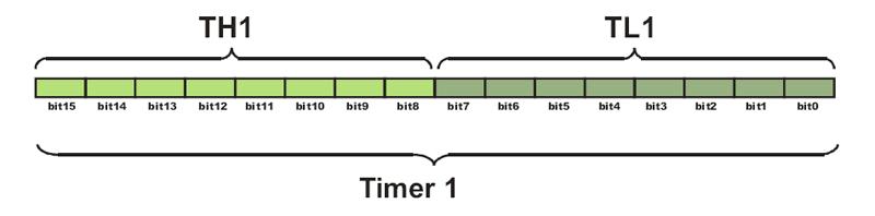
33 Counters and Timers: As you already know, the microcontroller oscillator uses quartz crystal for its operation. As the frequency of this oscillator is precisely defined and very stable, pulses it generates are always of the same width, which makes them ideal for time measurement. Such crystals are also used in quartz watches. In order to measure time between two events it is sufficient to count up pulses coming from this oscillator. That is exactly what the timer does. If the timer is properly programmed, the value stored in its register will be incremented (or decremented) with each coming pulse, i.e. once per each machine cycle. A single machine-cycle instruction lasts for 12 quartz oscillator periods, which means that by embedding quartz with oscillator frequency of 12MHz, a number stored in the timer register will be changed million times per second, i.e. each microsecond. The 8051 microcontroller has 2 timers/counters called T0 and T1. As their names suggest, their main purpose is to measure time and count external events. Besides, they can be used for generating clock pulses to be used in serial communication, so called Baud Rate. Timer T0 As seen in figure below, the timer T0 consists of two registers TH0 and TL0 representing a low and a high byte of one 16-digit binary number. Accordingly, if the content of the timer T0 is equal to 0 (T0=0) then both registers it consists of will contain 0. If the timer contains for example number 1000 (decimal), then the TH0 register (high byte) will contain the number 3, while the TL0 register (low byte) will contain decimal number 232. Formula used to calculate values in these two registers is very simple: TH TL0 = T Matching the previous example it would be as follows: = 1000

34 Since the timer T0 is virtually 16-bit register, the largest value it can store is In case of exceeding this value, the timer will be automatically cleared and counting starts from 0. This condition is called an overflow. Two registers TMOD and TCON are closely connected to this timer and control its operation. TMOD Register (Timer Mode) The TMOD register selects the operational mode of the timers T0 and T1. As seen in figure below, the low 4 bits (bit0 bit3) refer to the timer 0, while the high 4 bits (bit4 bit7) refer to the timer 1. There are 4 operational modes and each of them is described herein. Bits of this register have the following function: GATE1 enables and disables Timer 1 by means of a signal brought to the INT1 pin (P3.3): o 1 Timer 1 operates only if the INT1 bit is set. o 0 Timer 1 operates regardless of the logic state of the INT1 bit. C/T1 selects pulses to be counted up by the timer/counter 1: o 1 Timer counts pulses brought to the T1 pin (P3.5). o 0 Timer counts pulses from internal oscillator. T1M1,T1M0 These two bits select the operational mode of the Timer 1. T1M1 T1M0 MODE DESCRIPTION bit timer bit timer bit auto-reload Split mode GATE0 enables and disables Timer 1 using a signal brought to the INT0 pin (P3.2):
. o 0 Timer counts pulses from internal oscillator.")
35 o 1 Timer 0 operates only if the INT0 bit is set. o 0 Timer 0 operates regardless of the logic state of the INT0 bit. C/T0 selects pulses to be counted up by the timer/counter 0: o 1 Timer counts pulses brought to the T0 pin (P3.4). o 0 Timer counts pulses from internal oscillator. T0M1, T0M0 These two bits select the oprtaional mode of the Timer 0. T0M1 T0M0 MODE DESCRIPTION bit timer bit timer bit auto-reload Split mode Timer 0 in mode 0 (13-bit timer) This is one of the rarities being kept only for the purpose of compatibility with the previuos versions of microcontrollers. This mode configures timer 0 as a 13-bit timer which consists of all 8 bits of TH0 and the lower 5 bits of TL0. As a result, the Timer 0 uses only 13 of 16 bits. How does it operate? Each coming pulse causes the lower register bits to change their states. After receiving 32 pulses, this register is loaded and automatically cleared, while the higher byte (TH0) is incremented by 1. This process is repeated until registers count up 8192 pulses. After that, both registers are cleared and counting starts from 0.
36 Timer 0 in mode 1 (16-bit timer) Mode 1 configures timer 0 as a 16-bit timer comprising all the bits of both registers TH0 and TL0. That s why this is one of the most commonly used modes. Timer operates in the same way as in mode 0, with difference that the registers count up to as allowable by the 16 bits. Timer 0 in mode 2 (Auto-Reload Timer) Mode 2 configures timer 0 as an 8-bit timer. Actually, timer 0 uses only one 8-bit register for counting and never counts from 0, but from an arbitrary value (0-255) stored in another (TH0) register. The following example shows the advantages of this mode. Suppose it is necessary to constantly count up 55 pulses generated by the clock. If mode 1 or mode 0 is used, It is necessary to write the number 200 to the timer registers and constantly check whether an overflow has occured, i.e. whether they reached the value 255. When it happens, it is necessary to rewrite the number 200 and repeat the whole procedure. The same procedure is automatically performed by the microcontroller if set in mode 2. In fact, only the TL0 register operates as a timer, while another (TH0) register stores the value from which the counting starts. When the TL0 register is loaded, instead of being cleared, the contents of TH0 will be reloaded to it. Referring to the previous example, in order to register each 55th pulse, the best solution is to write the number 200 to the TH0 register and configure the timer to operate in mode 2.

, now control the 8-bit Timer 1.")
37 Timer 0 in Mode 3 (Split Timer) Mode 3 configures timer 0 so that registers TL0 and TH0 operate as separate 8-bit timers. In other words, the 16-bit timer consisting of two registers TH0 and TL0 is split into two independent 8-bit timers. This mode is provided for applications requiring an additional 8-bit timer or counter. The TL0 timer turns into timer 0, while the TH0 timer turns into timer 1. In addition, all the control bits of 16-bit Timer 1 (consisting of the TH1 and TL1 register), now control the 8-bit Timer 1. Even though the 16-bit Timer 1 can still be configured to operate in any of modes (mode 1, 2 or 3), it is no longer possible to disable it as there is no control bit to do it. Thus, its operation is restricted when timer 0 is in mode 3. The only application of this mode is when two timers are used and the 16-bit Timer 1 the operation of which is out of control is used as a baud rate generator.
38 Timer Control (TCON) Register TCON register is also one of the registers whose bits are directly in control of timer operation. Only 4 bits of this register are used for this purpose, while rest of them is used for interrupt control to be discussed later. TF1 bit is automatically set on the Timer 1 overflow. TR1 bit enables the Timer 1. o o 1 Timer 1 is enabled. 0 Timer 1 is disabled. TF0 bit is automatically set on the Timer 0 overflow. TR0 bit enables the timer 0. o o How to use the Timer 0? 1 Timer 0 is enabled. 0 Timer 0 is disabled. In order to use timer 0, it is first necessary to select it and configure the mode of its operation. Bits of the TMOD register are in control of it: Referring to figure above, the timer 0 operates in mode 1 and counts pulses generated by internal clock the frequency of which is equal to 1/12 the quartz frequency. Turn on the timer:

39 The TR0 bit is set and the timer starts operation. If the quartz crystal with frequency of 12MHz is embedded then its contents will be incremented every microsecond. After microseconds, the both registers the timer consists of will be loaded. The microcontroller automatically clears them and the timer keeps on repeating procedure from the beginning until the TR0 bit value is logic zero (0). How to read a timer? Depending on application, it is necessary either to read a number stored in the timer registers or to register the moment they have been cleared. It is extremely simple to read a timer by using only one register configured in mode 2 or 3. It is sufficient to read its state at any moment. That s all! It is somehow complicated to read a timer configured to operate in mode 2. Suppose the lower byte is read first (TL0), then the higher byte (TH0). The result is: TH0 = 15 TL0 = 255 Everything seems to be ok, but the current state of the register at the moment of reading was: TH0 = 14 TL0 = 255 In case of negligence, such an error in counting (255 pulses) may occur for not so obvious but quite logical reason. The lower byte is correctly read (255), but at the moment the program counter was about to read the higher byte TH0, an overflow occurred and the contents of both registers have been changed (TH0: 14 15, TL0: 255 0). This problem has a simple solution. The higher byte should be read first, then the lower byte and once again the higher byte. If the number stored in the higher byte is different then this sequence should be repeated. It s about a short loop consisting of only 3 instructions in the program. There is another solution as well. It is sufficient to simply turn the timer off while reading is going on (the TR0 bit of the TCON register should be cleared), and turn it on again after reading is finished.


40 Timer 0 Overflow Detection Usually, there is no need to constantly read timer registers. It is sufficient to register the moment they are cleared, i.e. when counting starts from 0. This condition is called an overflow. When it occurrs, the TF0 bit of the TCON register will be automatically set. The state of this bit can be constantly checked from within the program or by enabling an interrupt which will stop the main program execution when this bit is set. Suppose it is necessary to provide a program delay of 0.05 seconds ( machine cycles), i.e. time when the program seems to be stopped: First a number to be written to the timer registers should be calculated: Then it should be written to the timer registers TH0 and TL0: When enabled, the timer will resume counting from this number. The state of the TF0 bit, i.e. whether it is set, is checked from within the program. It happens at the moment of overflow, i.e. after exactly machine cycles or 0.05 seconds. How to measure pulse duration? Suppose it is necessary to measure the duration of an operation, for example how long a device has been turned on? Look again at the figure illustrating the timer and pay attention to the function of the GATE0 bit of the TMOD register. If it is cleared then the state of the P3.2 pin doesn t affect timer operation. If GATE0 = 1 the timer will operate until the pin P3.2 is cleared. Accordingly, if this pin is supplied with 5V through some external switch at the moment the device is being turned on, the timer will measure duration of its operation, which actually was the objective.
.")
41 How to count up pulses? Similarly to the previous example, the answer to this question again lies in the TCON register. This time it s about the C/T0 bit. If the bit is cleared the timer counts pulses generated by the internal oscillator, i.e. measures the time passed. If the bit is set, the timer input is provided with pulses from the P3.4 pin (T0). Since these pulses are not always of the same width, the timer cannot be used for time measurement and is turned into a counter, therefore. The highest frequency that could be measured by such a counter is 1/24 frequency of used quartz-crystal. Timer 1 Timer 1 is identical to timer 0, except for mode 3 which is a hold-count mode. It means that they have the same function, their operation is controlled by the same registers TMOD and TCON and both of them can operate in one out of 4 different modes.
42
e-pg Pathshala Subject : Computer Science Paper: Embedded System Module: 8051 Architecture Module No: CS/ES/5 Quadrant 1 e-text
 e-pg Pathshala Subject : Computer Science Paper: Embedded System Module: 8051 Architecture Module No: CS/ES/5 Quadrant 1 e-text In this lecture the detailed architecture of 8051 controller, register bank,
8051 MICROCONTROLLER
 8051 MICROCONTROLLER Mr.Darshan Patel M.Tech (Power Electronics & Drives) Assistant Professor Department of Electrical Engineering Sankalchand Patel College of Engineering-Visnagar WHY DO WE NEED TO LEARN
8051 Microcontroller Interrupts
 8051 Microcontroller Interrupts There are five interrupt sources for the 8051, which means that they can recognize 5 different events that can interrupt regular program execution. Each interrupt can be
Memory Organization. Program Memory
 Memory Organization The 8051 has two types of memory and these are Program Memory and Data Memory. Program Memory (ROM) is used to permanently save the program being executed, while Data Memory (RAM) is
EEE3410 Microcontroller Applications Department of Electrical Engineering Lecture 4 The 8051 Architecture
 Department of Electrical Engineering Lecture 4 The 8051 Architecture 1 In this Lecture Overview General physical & operational features Block diagram Pin assignments Logic symbol Hardware description Pin
8051 Microcontroller
 8051 Microcontroller The 8051, Motorola and PIC families are the 3 leading sellers in the microcontroller market. The 8051 microcontroller was originally developed by Intel in the late 1970 s. Today many
Fig 1. Block diagram of a microcomputer
 MICRO CONTROLLERS www.bookspar.com VTU NOTES QUESTION PAPERS UNIT - 1 Computer: A computer is a multipurpose programmable machine that reads binary instructions from its memory, accepts binary data as
UNIT 5. Microcontrollers. Syllabus
 UNIT 5 Microcontrollers Syllabus Architecture of 8051 Signals Operational features Memory and I/O addressing Interrupts Instruction set Applications. OVERVIEW The past three decades have seen the introduction
8-bit Microcontroller with 8K Bytes In-System Programmable Flash AT89S52
 Features Compatible with MCS -51 Products 8K Bytes of In-System Programmable (ISP) Flash Memory Endurance: 10,000 Write/Erase Cycles 4.0V to 5.5V Operating Range Fully Static Operation: 0 Hz to 33 MHz
UNIT IV MICROCONTROLLER
 UNIT IV 8051- MICROCONTROLLER Prepared by R. Kavitha Page 1 Application Prepared by R. Kavitha Page 2 Pin Description of the 8051 UNIT IV- 8051 MICROCONTROLLER P1.0 P1.1 P1.2 P1.3 P1.4 P1.5 P1.6 P1.7 RST
UNIT MICROCONTROLLER AND ITS PROGRAMMING
 M i c r o p r o c e s s o r s a n d M i c r o c o n t r o l l e r s P a g e 1 UNIT-7 8051 MICROCONTROLLER AND ITS PROGRAMMING INTRODUCTION The microcontroller incorporates all the features that are found
The Microcontroller. Lecture Set 3. Major Microcontroller Families. Example Microcontroller Families Cont. Example Microcontroller Families
 The Microcontroller Lecture Set 3 Architecture of the 8051 Microcontroller Microcontrollers can be considered as self-contained systems with a processor, memory and I/O ports. In most cases, all that is
Module I. Microcontroller can be classified on the basis of their bits processed like 8bit MC, 16bit MC.
 MICROCONTROLLERS AND APPLICATIONS 1 Module 1 Module I Introduction to Microcontrollers: Comparison with Microprocessors Harvard and Von Neumann Architectures - 80C51 microcontroller features - internal
MICROPROCESSORS AND MICROCONTROLLERS MATERIAL. Features of 8051:
 DEPARTMENT OF ECE MICROPROCESSORS AND MICROCONTROLLERS MATERIAL UNIT V 8051 MICROCONTROLLERS To make a complete microcomputer system, only microprocessor is not sufficient. It is necessary to add other
8051 Microcontroller
 8051 Microcontroller 1 Salient Features (1). 8 bit microcontroller originally developed by Intel in 1980. (2). High-performance CMOS Technology. (3). Contains Total 40 pins. (4). Address bus is of 16 bit
Understanding the basic building blocks of a microcontroller device in general. Knows the terminologies like embedded and external memory devices,
 Understanding the basic building blocks of a microcontroller device in general. Knows the terminologies like embedded and external memory devices, CISC and RISC processors etc. Knows the architecture and
THE 8051 MICROCONTROLLER Simple comparison: Pentium vs. 8051
 THE 8051 MICROCONTROLLER Simple comparison: Pentium vs. 8051 FEATURE 8051 PENTIUM COMMENT Clock Speed 12Mhz. typical 1,000 MHz. (1GHz.) but 60MHz. ICs available 8051 internally divides clock by 12 so for
CS 320. Computer Architecture Core Architecture
 CS 320 Computer Architecture 8051 Core Architecture Evan Hallam 19 April 2006 Abstract The 8051 is an 8-bit microprocessor designed originally in the 1980 s by the Intel Corporation. This inexpensive and
EE6502- MICROPROCESSOR AND MICROCONTROLLER
 . EE6502- MICROPROCESSOR AND MICROCONTROLLER UNIT III - 8051 MICROCONTROLLER PART - A 1. What is Microcontroller? A device which contains the microprocessor with integrated peripherals like memory, serial
8051 microcontrollers
 8051 microcontrollers Presented by: Deepak Kumar Rout Synergy Institute of Engineering and Technology, Dhenkanal Chapter 2 Introduction Intel MCS-51 family of microcontrollers consists of various devices
8051 Microcontrollers
 8051 Microcontrollers Richa Upadhyay Prabhu NMIMS s MPSTME richa.upadhyay@nmims.edu March 8, 2016 Controller vs Processor Controller vs Processor Introduction to 8051 Micro-controller In 1981,Intel corporation
ISSI. IS89C51 CMOS SINGLE CHIP 8-BIT MICROCONTROLLER with 4-Kbytes of FLASH ISSI IS89C51 NOVEMBER 1998 FEATURES GENERAL DESCRIPTION
 IS89C51 CMOS SINGLE CHIP 8-BIT MICROCONTROLLER with 4-Kbytes of FLASH NOVEMBER 1998 FEATURES 80C51 based architecture 4-Kbytes of on-chip Reprogrammable Flash Memory 128 x 8 RAM Two 16-bit Timer/Counters
 Distributed by: www.jameco.com 1-800-831-4242 The content and copyrights of the attached material are the property of its owner. 8051 8052 and 80C51 Hardware Description December 1992 Order Number 270252-006
Rev. No. History Issue Date Remark
 Preliminary Bar Code Reader Document Title Bar Code Reader Revision History Rev. No. History Issue Date Remark 0.0 Initial issue June 5, 2000 Preliminary 0.1 Change document title from Bar Code Reader
Serial I-O for Dinesh K. Sharma Electrical Engineering Department I.I.T. Bombay Mumbai (version 14/10/07)
") Serial I-O for 8051 Dinesh K. Sharma Electrical Engineering Department I.I.T. Bombay Mumbai 400 076 (version 14/10/07) 1 Motivation Serial communications means sending data a single bit at a time. But
Serial I-O for 8051 Dinesh K. Sharma Electrical Engineering Department I.I.T. Bombay Mumbai 400 076 (version 14/10/07) 1 Motivation Serial communications means sending data a single bit at a time. But
Memory organization Programming model - Program status word - register banks - Addressing modes - instruction set Programming examples.
 MICROCONTROLLERS AND APPLICATIONS 1 Module 2 Module-2 Contents: Memory organization Programming model - Program status word - register banks - Addressing modes - instruction set Programming examples. MEMORY
The Timers/Counters The Serial Interface The Interrupt System Reset P0.0-P0.7 P2.0-P2.7. Port 2 Drivers. Port 2 Latch
 HARDWARE DESCRIPTION This chapter provides a detailed description of the 80C51 microcontroller (see Figure 1). Included in this description are: The port drivers and how they function both as ports and,
8051 Serial Communication
 8051 Serial Communication Basics of serial communication Parallel: transfers eight bits of data simultaneously over eight data lines expensive - short distance fast Serial : one bit at a time is transferred
Question Bank Microprocessor and Microcontroller
 QUESTION BANK - 2 PART A 1. What is cycle stealing? (K1-CO3) During any given bus cycle, one of the system components connected to the system bus is given control of the bus. This component is said to
MICROPROCESSOR & MICROCONTROLLER
 a) From road north to East From road east to north From road south to west From road west to south From road west to north b) From road north to East From road south to west From road south to north From
UNIT MICROCONTROLLER
 Page UNIT-5 805 MICROCONTROLLER INTRODUCTION The microcontroller incorporates all the features that are found in microprocessor. The microcontroller has built in ROM, RAM, Input Output ports, Serial Port,
MCS-51 Serial Port A T 8 9 C 5 2 1
 MCS-51 Serial Port AT89C52 1 Introduction to Serial Communications Serial vs. Parallel transfer of data Simplex, Duplex and half-duplex modes Synchronous, Asynchronous UART Universal Asynchronous Receiver/Transmitter.
Timer-1 can be run using the internal clock, fosc/12 (timer mode) or from any external source via pin T1 (P3.5) (Counter mode).
 or from any external source via pin T1 (P3.5) (Counter mode).") EC 6504 MICROPROCESSOR AND MICROCONTROLLER Electronics and Communication Engineering Fifth Semester UNIT-V Part A 1. List the modes of Timer in 8051. [N/D16] The timers available in 8051 are Timer 0 (T0)
EC 6504 MICROPROCESSOR AND MICROCONTROLLER Electronics and Communication Engineering Fifth Semester UNIT-V Part A 1. List the modes of Timer in 8051. [N/D16] The timers available in 8051 are Timer 0 (T0)
8051 Microcontroller memory Organization and its Applications
 8051 Microcontroller memory Organization and its Applications Memory mapping in 8051 ROM memory map in 8051 family 0000H 4k 0000H 8k 0000H 32k 0FFFH DS5000-32 8051 1FFFH 8752 7FFFH from Atmel Corporation
Fig 1. Block diagram of a microcomputer
 Computer: A computer is a multipurpose programmable machine that reads binary instructions from its memory, accepts binary data as input,processes the data according to those instructions and provides
MAHALAKSHMI ENGINEERING COLLEGE TIRUCHIRAPALLI
 MAHALAKSHMI ENGINEERING COLLEGE TIRUCHIRAPALLI-621213. QUESTION BANK DEPARTMENT: EEE SUB CODE: EE2324 YR/ SEM:III/ VI SUB NAME: MICROPROCESSORS & MICROCONTROLLERS UNIT 4-8051 MICROCONTROLLER PART A (2
CoE3DJ4 Digital Systems Design. Chapter 5: Serial Port Operation
 CoE3DJ4 Digital Systems Design Chapter 5: Serial Port Operation Serial port 8051 includes an on-chip serial port Hardware access to the port is through TXD and RXD (Port 3 bits 1 and 0) Serial port is
8051 Overview and Instruction Set
 8051 Overview and Instruction Set Curtis A. Nelson Engr 355 1 Microprocessors vs. Microcontrollers Microprocessors are single-chip CPUs used in microcomputers Microcontrollers and microprocessors are different
Vidyalankar T.E. Sem. V [ETRX] Microprocessors and Microcontrollers I Prelim Question Paper Solution
![Vidyalankar T.E. Sem. V [ETRX] Microprocessors and Microcontrollers I Prelim Question Paper Solution](/thumbs/74/70555699.jpg "Vidyalankar T.E. Sem. V [ETRX] Microprocessors and Microcontrollers I Prelim Question Paper Solution") 1. (a) 1. (b) T.E. Sem. V [ETRX] Microprocessors and Microcontrollers I Prelim Question Paper Solution Priority modes. 1) Fully Nested Mode : It is a general purpose mode. IR 0 highest priority IR 1 lowest
1. (a) 1. (b) T.E. Sem. V [ETRX] Microprocessors and Microcontrollers I Prelim Question Paper Solution Priority modes. 1) Fully Nested Mode : It is a general purpose mode. IR 0 highest priority IR 1 lowest
MICROCONTROLLER AND PLC LAB-436 SEMESTER-5
 MICROCONTROLLER AND PLC LAB-436 SEMESTER-5 Exp:1 STUDY OF MICROCONTROLLER 8051 To study the microcontroller and familiarize the 8051microcontroller kit Theory:- A Microcontroller consists of a powerful
INTEGRATED CIRCUITS DATA SHEET. P89C738; P89C739 8-bit microcontrollers Dec 15. Product specification File under Integrated Circuits, IC20
 INTEGRATED CIRCUITS DATA SHEET File under Integrated Circuits, IC20 1997 Dec 15 CONTENTS 1 FEATURES 2 GENERAL DESCRIPTION 3 ORDERING INFORMATION 4 BLOCK DIAGRAM 5 FUNCTIONAL DIAGRAM 6 PINNING INFORMATION
MODULE-1. Short Answer Questions
 MODULE-1 Short Answer Questions 1. Give the comparison between microprocessor and microcontroller. It is very clear from figure that in microprocessor we have to interface additional circuitry for providing
Lecture 1. Course Overview and The 8051 Architecture
 Lecture 1 Course Overview and The 8051 Architecture MCUniversity Program Lectures 8051 architecture t System overview of C8051F020 8051 instruction set System clock, crossbar and GPIO Assembler directives
 8051 Memory Organization BY D. BALAKRISHNA, Research Assistant, IIIT-H Chapter 1: Memory Organization There are 2 types of memories available in 8051 microcontroller. Program memory/c code memory (ROM)
8XC51RA RB RC Hardware Description
 8XC51RA RB RC Hardware Description February 1995 Order Number 272668-001 Information in this document is provided in connection with Intel products Intel assumes no liability whatsoever including infringement
Three criteria in Choosing a Microcontroller
 The 8051 Microcontroller architecture Contents: Introduction Block Diagram and Pin Description of the 8051 Registers Some Simple Instructions Structure of Assembly language and Running an 8051 program
Module Contents of the Module Hours COs
 Microcontrollers (EE45): Syllabus: Module Contents of the Module Hours COs 1 8051 MICROCONTROLLER ARCHITECTURE: Introduction to Microprocessors and Microcontrollers, the 8051 Architecture, 08 1 and pin
MAHALAKSHMI ENGINEERING COLLEGE TIRUCHIRAPALLI UNIT- IV
 UNIT- IV PART A (2 MARK QUESTIONS) 1. What is the need for de-bouncing the keyboard? (AUC NOV 2012) Debouncing is any kind of hardware device or software that ensures that only a single signal will be
The Final Word on 8051 Microcontroller
 The Final Word on 8051 Microcontroller This is a book about the Intel 8051 microcontroller and its large family of descendants. It is intended to give you, the reader, some new techniques for optimizing
UNIT V MICRO CONTROLLER PROGRAMMING & APPLICATIONS TWO MARKS. 3.Give any two differences between microprocessor and micro controller.
 UNIT V -8051 MICRO CONTROLLER PROGRAMMING & APPLICATIONS TWO MARKS 1. What is micro controller? Micro controller is a microprocessor with limited number of RAM, ROM, I/O ports and timer on a single chip
SYLLABUS UNIT - I 8086/8088 ARCHITECTURE AND INSTRUCTION SET
 1 SYLLABUS UNIT - I 8086/8088 ARCHITECTURE AND INSTRUCTION SET Intel 8086/8088 Architecture Segmented Memory, Minimum and Maximum Modes of Operation, Timing Diagram, Addressing Modes, Instruction Set,
ENE 334 Microprocessors
 Page 1 ENE 334 Microprocessors Lecture 7: MCS-51 Architecture I : Dejwoot KHAWPARISUTH http://webstaff.kmutt.ac.th/~dejwoot.kha/ ENE 334 MCS-51 Architecture I Page 2 Outlines: 8051 Microcontroller Hardware
DATA SHEET. P80CL31; P80CL51 Low voltage 8-bit microcontrollers with UART INTEGRATED CIRCUITS Apr 15
 INTEGRATED CIRCUITS DATA SHEET Low voltage 8-bit microcontrollers with Supersedes data of January 1995 File under Integrated circuits, IC20 1997 Apr 15 CONTENTS 1 FEATURES 2 GENERAL DESCRIPTION 2.1 Versions:
Microcontrollers. Fig. 1 gives a comparison of a microprocessor system and a microcontroller system.
 Syllabus: : Introduction to, 8051 Microcontroller Architecture and an example of Microcontroller based stepper motor control system (only Block Diagram approach). (5 Hours) Introduction to A microcontroller
8051 Core Specification
 8051 Core Specification Authors: Jaka Simsic Simon Teran jakas@opencores.org simont@opencores.org Rev. 0.1 August 14, 2001 First Draft www.opencores.org Rev 0.1 First Draft 1 of 26 Revision History Rev.
Embedded World Television, Radio, CD player, Washing Machine Microwave Oven Card readers, Palm devices
 A presentation on INTRODUCTION We are living in the Embedded World. We are surrounded with many embedded products and our daily life largely depends on the proper functioning of these gadgets. Television,
SOLUTION MANUAL FOR THE 8051 MICROCONTROLLER 4TH EDITION BY MACKENZIE AND PHAN
 SOLUTION MANUAL FOR THE 8051 MICROCONTROLLER 4TH EDITION BY MACKENZIE AND PHAN Chapter 1 - Introduction to Microcontrollers 1. (a)the first widely used microprocessor was the 8080. (b) The 8080 was introduced
Architecture & Instruction set of 8085 Microprocessor and 8051 Micro Controller
 of 8085 microprocessor 8085 is pronounced as "eighty-eighty-five" microprocessor. It is an 8-bit microprocessor designed by Intel in 1977 using NMOS technology. It has the following configuration 8-bit
CPEG300 Embedded System Design. Lecture 3 Memory
 CPEG300 Embedded System Design Lecture 3 Memory Hamad Bin Khalifa University, Spring 2018 Review Von Neumann vs. Harvard architecture? System on Board, system on chip? Generic Hardware Architecture of
Introduction To MCS-51
 Introduction To MCS-51 By Charoen Vongchumyen Department of Computer Engineering Faculty of Engineering KMITLadkrabang 8051 Hardware Basic Content Overview Architechture Memory map Register Interrupt Timer/Counter
1. INTRODUCTION TO MICROPROCESSOR AND MICROCOMPUTER ARCHITECTURE:
 1. INTRODUCTION TO MICROPROCESSOR AND MICROCOMPUTER ARCHITECTURE: A microprocessor is a programmable electronics chip that has computing and decision making capabilities similar to central processing unit
VRS540-4kB Flash, 128B RAM, 25~40MHz, 8-Bit MCU
 VRS540-4kB Flash, 28B RAM, 25~40MHz, 8-Bit MCU 34 Ste Catherine Street West, Suite 900, Montreal, Quebec, Canada H3B H4 Tel: (54) 87-2447 http://www.goalsemi.com P.3 P.2 XTAL NC P0./AD VRS540 Overview
MSM80C154S MSM83C154S MSM85C154HVS USER'S MANUAL
 MSM8C54S MSM83C54S MSM85C54HVS USER'S MANUAL Copyright 988, OKI ELECTRIC INDUSTRY COMPANY, LTD. OKI makes no warranty for the use of its products and assumes no responsibility for any errors which may
VRS550-8kB Flash, 256B RAM, 25~40MHz, 8-Bit MCU VRS560-16kB Flash, 256B RAM, 40MHz, 8-Bit MCU
 VRS550-8kB Flash, 256B RAM, 25~40MHz, 8-Bit MCU VRS560-6kB Flash, 256B RAM, 40MHz, 8-Bit MCU 34 Ste Catherine Street West, Suite 900, Montreal, Quebec, Canada H3B H4 Tel: (54) 87-2447 http://www.goalsemi.com
Handshake Solutions. HT80C51 User Manual
 HT8C5 User Manual HT8C5 User Manual Document Information Document Information Document Title Date of Creation 27/6/25 Date of last change 27/6/25 File name Status Version Number.7 Client / Target Audience
Embedded Controller Programming
 Embedded Controller Programming Counters, Timers and I/O in Assembly Language Ken Arnold Copyright 2000-2004 Ken Arnold 1 Outline Timer/Counters Serial Port More 8051 Instructions Examples Copyright 2000-2004
Preliminary W77E58 8 BIT MICROCONTROLLER. Table of Contents-- Publication Release Date: March Revision A1
 8 BIT MICROCONTROLLER Table of Contents-- GENERAL DESCRIPTION...2 FEATURES...2 PIN CONFIGURATION...3 PIN DESCRIPTION...4 BLOCK DIAGRAM...6 FUNCTIONAL DESCRIPTION...7 MEMORY ORGANIZATION...8 INSTRUCTION...29
8051 Timers and Serial Port
 8051 Timers and Serial Port EE4380 Fall 2001 Class 10 Pari vallal Kannan Center for Integrated Circuits and Systems University of Texas at Dallas Timer: Mode 1 Operation (recap) 16 bit counter. Load the
Control Unit: The control unit provides the necessary timing and control Microprocessor resembles a CPU exactly.
 Unit I 8085 and 8086 PROCESSOR Introduction to microprocessor A microprocessor is a clock-driven semiconductor device consisting of electronic logic circuits manufactured by using either a large-scale
W77IE58 8-BIT MICROCONTROLLER. Table of Contents-- Publication Release Date: December Revision A2
 8-BIT MICROCONTROLLER Table of Contents-- GENERAL DESCRIPTION... 2 FEATURES... 2 PIN CONFIGURATIONS... 3 PIN DESCRIPTION... 4 BLOCK DIAGRAM... 6 FUNCTIONAL DESCRIPTION... 7 MEMORY ORGANIZATION... 8 Instruction...
7.2.1 Timer 2 Capture LSB... 24
 Data Sheet 8-BIT MICROCONTROLLER Table of Contents-. GENERAL DESCRIPTION... 3 2. FEATURES... 3 3. PIN CONFIGURATIONS... 4 4. PIN DESCRIPTION... 5 5. FUNCTIONAL DESCRIPTION... 6 6. MEMORY ORGANIZATION...
b. List different system buses of 8085 microprocessor and give function of each bus. (8) Answer:
 Answer:") Q.2 a. Discuss and differentiate between a Microprocessor and a Microcontroller. Microprocessor is an IC which has only the CPU inside them i.e. only the processing powers such as Intel s Pentium 1,2,3,4,
Q.2 a. Discuss and differentiate between a Microprocessor and a Microcontroller. Microprocessor is an IC which has only the CPU inside them i.e. only the processing powers such as Intel s Pentium 1,2,3,4,
WINTER 14 EXAMINATION
 Subject Code: 17534 WINTER 14 EXAMINATION Model Answer Important Instructions to examiners: 1) The answers should be examined by key words and not as word-to-word as given in the model answer scheme. 2)
Interrupt Programming: Interrupts vs. Polling Method:
 UNIT 4: INTERRUPT PROGRAMMING & SERIAL COMMUNICATION WITH 8051: Definition of an interrupt, types of interrupts, Timers and Counter programming with interrupts in assembly. 8051 Serial Communication: Data
Chapter C2051 Architecture and Serial Communication Link
 Chapter- 2 89C2051 Architecture and Serial Communication Link ABSTRACT This chapter provides the details of 89C2051 microcontroller and description on Serial Communication Facility presented by 89C2051
MCS -51 Programmer s Guide and Instruction Set
 MCS -51 Programmer s Guide and Instruction Set November 1992 Order Number 270249-003 COPYRIGHT INTEL CORPORATION 1996 MCS -51 PROGRAMMER S GUIDE AND INSTRUCTION SET CONTENTS PAGE MEMORY ORGANIZATION 1
Microcomputer Architecture and Programming
 IUST-EE (Chapter 1) Microcomputer Architecture and Programming 1 Outline Basic Blocks of Microcomputer Typical Microcomputer Architecture The Single-Chip Microprocessor Microprocessor vs. Microcontroller
Serial communication
 Serial communication CSCI 255: Introduction to Embedded Systems Keith Vertanen Copyright 2011 Serial communication Terminology RS-232 protocol Baud rates Flow control Example Overview Develop functions
AT Bit Spread- Spectrum Microcontroller. Preliminary. Features. Description. Pin Configuration
 Features Compatible with MCS-51 Products 8K bytes of On-Board Program Memory Fully Static Operation: 0 Hz to 16 MHz 256 x 8 Bit Internal RAM 32 Programmable I/O Lines Three 16 Bit Timer/Counters Eight
SUMMER 13 EXAMINATION
 MAHARASHTRA STATE BOARD OF TECHNICAL EDUCATION (Autonomous) (ISO/IEC - 27001-2005 Certified) Subject Code: 12187 SUMMER 13 EXAMINATION Model Answer Important Instructions to examiners: 1) The answers should
80C51 family programmer s guide and instruction set. 80C51 Family. PROGRAMMER S GUIDE AND INSTRUCTION SET Memory Organization. Philips Semiconductors
 PROGRAMMER S GUIDE AND INSTRUCTION SET Memory Organization Program Memory The 80C51 has separate address spaces for program and data memory. The Program memory can be up to 64k bytes long. The lower 4k
SRL0 Serial Port Unit
 Summary The serial communications port peripheral devices can be configured for communications between a microprocessor and peripheral devices, or for multiprocessor communications. This document provides
Moodle WILLINGDON COLLEGE SANGLI (B. SC.-II) Digital Electronics
 Digital Electronics") Moodle 4 WILLINGDON COLLEGE SANGLI (B. SC.-II) Digital Electronics Advanced Microprocessors and Introduction to Microcontroller Moodle developed By Dr. S. R. Kumbhar Department of Electronics Willingdon
Moodle 4 WILLINGDON COLLEGE SANGLI (B. SC.-II) Digital Electronics Advanced Microprocessors and Introduction to Microcontroller Moodle developed By Dr. S. R. Kumbhar Department of Electronics Willingdon
W77LE58/W77L058A Data Sheet 8-BIT MICROCONTROLLER. Table of Contents- Publication Release Date: April 17, Revision A7
 Data Sheet 8-BIT MICROCONTROLLER Table of Contents-. GENERAL DESCRIPTION... 2 2. FEATURES... 2 3. PIN CONFIGURATIONS... 3 4. PIN DESCRIPTION... 4 5. FUNCTIONAL DESCRIPTION... 5 6. MEMORY ORGANIZATION...
Microcontroller and Embedded Systems:
 Microcontroller and Embedded Systems: Branches: 1. Electronics & Telecommunication Engineering 2. Electrical & Electronics Engineering Semester: 6 th Semester / 7 th Semester 1. Explain the differences
EXPERIMENT NO.1. A Microcontroller is a complete computer system built on a single chip.
 EXPERIMENT NO.1 AIM: Study of 8051 Microcontroller TOOLS: 8051 kit THEORY: Salient Features of 8051 A Microcontroller is a complete computer system built on a single chip. It contains all components like
Chapter 1: Basics of Microprocessor [08 M]
![Chapter 1: Basics of Microprocessor [08 M]](/thumbs/77/75860546.jpg "Chapter 1: Basics of Microprocessor [08 M]") Microprocessor: Chapter 1: Basics of Microprocessor [08 M] It is a semiconductor device consisting of electronic logic circuits manufactured by using either a Large scale (LSI) or Very Large Scale (VLSI)
Microprocessor: Chapter 1: Basics of Microprocessor [08 M] It is a semiconductor device consisting of electronic logic circuits manufactured by using either a Large scale (LSI) or Very Large Scale (VLSI)
SANKALCHAND PATEL COLLEGE OF ENGINEERING, VISNAGAR. ELECTRONICS & COMMUNICATION DEPARTMENT Question Bank- 1
 SANKALCHAND PATEL COLLEGE OF ENGINEERING, VISNAGAR ELECTRONICS & COMMUNICATION DEPARTMENT Question Bank- 1 Subject: Microcontroller and Interfacing (151001) Class: B.E.Sem V (EC-I & II) Q-1 Explain RISC
W77E058A Data Sheet 8-BIT MICROCONTROLLER. Table of Contents-
 Data Sheet 8-BIT MICROCONTROLLER Table of Contents-. GENERAL DESCRIPTION... 3 2. FEATURES... 3 3. PIN CONFIGURATIONS... 4 4. PIN DESCRIPTION... 5 5. FUNCTIONAL DESCRIPTION... 7 6. MEMORY ORGANIZATION...
Mod-3: Interrupts,Timer operation,serial communication 1
 Mod-3: Interrupts,Timer operation,serial communication 1 Module-3 Contents: Interrupts - interrupt sources - interrupt handling programming examples. Timers operation different modes waveform generation-
MASSEY UNIVERSITY PALMERSTON NORTH CAMPUS
 MASSEY UNIVERSITY PALMERSTON NORTH CAMPUS EXAMINATION FOR 159.233 COMPUTER SYSTEMS Semester One June 2008 Time allowed: THREE (3) hours This exam contains THREE (3) questions ANSWER ALL THREE (3) QUESTIONS
Q.1. A) Attempt any THREE of the following:
 Attempt any THREE of the following:") Important Instructions to examiners: 1) The answers should be examined by key words and not as word-to-word as given in the model answer scheme. 2) The model answer and the answer written by candidate
Important Instructions to examiners: 1) The answers should be examined by key words and not as word-to-word as given in the model answer scheme. 2) The model answer and the answer written by candidate
ELEG3923 Microprocessor Ch.10 Serial Port Programming
 Department of Electrical Engineering University of Arkansas ELEG3923 Microprocessor Ch.10 Serial Port Programming Dr. Jingxian Wu wuj@uark.edu OUTLINE 2 Basics of Serial Communication Serial port programming
Module 3. Embedded Systems I/O. Version 2 EE IIT, Kharagpur 1
 Module 3 Embedded Systems I/O Version 2 EE IIT, Kharagpur 1 Lesson 15 Interrupts Version 2 EE IIT, Kharagpur 2 Instructional Objectives After going through this lesson the student would learn Interrupts
EC Microprocessor and Microcontroller
 DMI COLLEGE OF ENGINEERING EC6504 - Microprocessor and Microcontroller UNIT I THE 8086 MICROPROCESSOR 1. What are different data transfer schemes? The different data transfer schemes are [A/M 12] 2. How
8XC151SA and 8XC151SB Hardware Description
 8XC151SA and 8XC151SB Hardware Description June 1996 Order Number 272832-001 Information in this document is provided in connection with Intel products Intel assumes no liability whatsoever including infringement
Engr. A. N. Aniedu Electronic and Computer Engineering Nnamdi Azikiwe University, Awka
 Engr. A. N. Aniedu Electronic and Computer Engineering Nnamdi Azikiwe University, Awka INTRODUCTION Microcontroller vs General Purpose Microprocessor General-purpose microprocessors contains No RAM No
Preliminary W77C32 8 BIT MICROCONTROLLER GENERAL DESCRIPTION FEATURES
 GENERAL DESCRIPTION 8 BIT MICROCONTROLLER The W77C32 is a fast 805 compatible microcontroller with a redesigned processor core without wasted clock and memory cycles. As a result, it executes every 805
MICROCONTROLLER UNIT 1
 MICROCONTROLLER UNIT 1 OUTLINE INTRODUCTION MICROCONTROLLERS AND EMBEDDED PROCESSORS OVERVIEW OF THE 8051 8051 MICTROCONTROLLER HARDWARE ADDRESSING MODES INTRODUCTION The first task to use a new computer
Microcontrollers can be considered as self-contained systems with a processor, memory and I/O ports.
 8051 Architecture 1 Microcontrollers can be considered as self-contained systems with a processor, memory and I/O ports. In most cases, all that is missing is the software to define the operation of the