MAHALAKSHMI ENGINEERING COLLEGE TIRUCHIRAPALLI
|
|
|
- Hilary Edwards
- 6 years ago
- Views:
Transcription
 1.")
 *128 data memory on chip. *Four register banks. *Two multiple mode,16-bit timer/counter. *Extensive Boolean processing capabilities.")
1 MAHALAKSHMI ENGINEERING COLLEGE TIRUCHIRAPALLI QUESTION BANK DEPARTMENT: EEE SUB CODE: EE2324 YR/ SEM:III/ VI SUB NAME: MICROPROCESSORS & MICROCONTROLLERS UNIT MICROCONTROLLER PART A (2 Marks) 1. What are the main features of 8051 microcontroller?(auc MAY 2012) The features are *single supply +5 volt operation using HMOS technology. *4096 bytes program memory on chip (not on 8031) *128 data memory on chip. *Four register banks. *Two multiple mode,16-bit timer/counter. *Extensive Boolean processing capabilities. *64 KB external RAM size *32 bi-directional individually addressable I/O lines. *8 bit CPU optimized for control applications 2. List the on chip peripherals of 8051 microcontroller. (AUC NOV 2011) 4KB on chip RAM 128 B RAM 2 Timers 32 I/O pins 1 serial port 6 Interrupt sources EE2324/ Microprocessors & Microcontrollers Department of EEE 1
2 3. What are the addressing modes of 8051 microcontroller? (AUC NOV 2011) Immediate Direct Register Register Indirect 4. List the alternative function assigned to port 3 pins of 8051 microcontroller. (AUC MAY 2011) P3 bit Function pin P3.0 RxD ( Receive data,serial communication) 10 P3.1 TxD(( Transmit data,serial communication) 11 P3.2 INT0 12 P3.3 INT1 13 P3.4 T0 14 P3.5 T1 15 P3.6 WR 16 P3.7 RD Mention the size of DPTR & stack pointer in 8051 microcontroller. (AUC MAY 2011) Size of stack Pointer & DPTR registers are 16 bit. PART B (8, 16Marks) 1. Explain with a neat block diagram the architecture of 8051 microcontroller. (AUC MAY 2012) EE2324/ Microprocessors & Microcontrollers Department of EEE 2

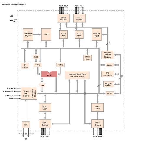
3 EE2324/ Microprocessors & Microcontrollers Department of EEE 3

4 EE2324/ Microprocessors & Microcontrollers Department of EEE 4

5 Pin Configuration: 8051: Types of Memory The 8051 has three very general types of memory. To effectively program the 8051 it is necessary to have a basic understanding of these memory types. EE2324/ Microprocessors & Microcontrollers Department of EEE 5
6 On-Chip Memory refers to any memory(code, RAM, or other) that physically exists on the microcontroller itself. On-chip memory can be of several types, but we'll get into that shortly. External Code Memory is code (or program) memory that resides off-chip. This is often in the form of an external EPROM. External RAM is RAM memory that resides off-chip. This is often in the form of standard static RAM or flash RAM. Code Memory Code memory is the memory that holds the actual 8051 program that is to be run. This memory is limited to 64K and comes in many shapes and sizes: Code memory may be found on-chip, either burned into the microcontroller as ROM or EPROM. Code may also be stored completely off-chip in an external ROM or, more commonly, an external EPROM. Flash RAM is also another popular method of storing a program. Various combinations of these memory types may also be used--that is to say, it is possible to have4k of code memory on-chip and 64k of code memory offchip in an EPROM. When the program is stored on-chip the 64K maximum is often reduced to 4k, 8k, or 16k. This varies depending on the version of the chip that is being used. Each version offers specific capabilities and one of the distinguishing factors from chip to chip is how much ROM/EPROM space the chip has. However, code memory is most commonly implemented as off-chip EPROM Programming Tip: Since code memory is restricted to 64K, 8051 programs are limited to 64K. Some assemblers and compilers offer ways to get around this limit when used with specially wired hardware. However, without such special compilers and hardware, programs are limited to 64K. External RAM As an obvious opposite of Internal RAM, the 8051 also supports what is called External RAM. As the name suggests, External RAM is any random access memory which is found off-chip. Since the memory is off-chip it is not as flexible in terms of accessing, and is also slower. For example, to increment an Internal RAM location by 1 requires only 1 instruction and 1 instruction cycle. To increment a 1-byte value stored in External RAM requires 4 instructions and 7 instruction cycles. In this case, external memory is 7 times slower! What External RAM loses in speed and flexibility EE2324/ Microprocessors & Microcontrollers Department of EEE 6
7 it gains in quantity? While Internal RAM is limited to 128 bytes the 8051 supports External RAM up to 64K. Programming Tip: The 8051 may only address 64k of RAM. To expand RAM beyond this limit requires programming and hardware tricks. You may have to do this "by hand" since many compilers and assemblers, while providing support for programs in excess of 64k, do not support more than 64k of RAM. This is rather strange since it has been my experience that programs can usually fit in 64k but often RAM is what is lacking. Thus if you need more than 64k of RAM, check to see if your compiler supports it-- but if it doesn't, be prepared to do it by hand. On-Chip Memory. The 8051 includes a certain amount of onchip memory. On-chip memory is really one of two (SFR) memories. the 8051 has bank of 128 bytes of Internal RAM. This Internal RAM is found on-chip on the 8051 so it is the fastest RAM available, and it is also the most flexible in terms of reading, writing, and modifying its contents. Internal RAM is volatile, so when the 8051 is reset this memory is cleared. The 128 bytes of internal ram is subdivided as shown on the memory map. The first 8 bytes (00h- 07h) are "register bank 0". By manipulating certain SFRs, a program may choose to use register banks1, 2, or 3. These alternative register banks are located in internal RAM in addresses 08h through1fh.the 80 bytes remaining of Internal RAM, from addresses 30h through 7Fh, may be used by user variables that need to be accessed frequently or at high-speed. This area is also utilized by the microcontroller as a storage area for the operating stack. This fact severely limits the 8051 s stack since, as illustrated in the memory map, the area reserved for the stack is only 80 bytes--and usually it is less since this 80 bytes has to be shared between the stack and user variables. Register Banks The 8051 uses 8 "R" registers which are used in many of its instructions. These "R"registers are numbered from 0 through 7 (R0, R1,R2, R3, R4, R5, R6, and R7). These registers are generally used to assist in manipulating values and moving data from one memory location to another. For example, to add the value of R4 to the Accumulator, we would execute the following instruction: ADD A,R4When the 8051 is first booted up, register bank 0(addresses 00h through 07h) is used by default. However, your program may instruct the 8051 to use one of the alternate register EE2324/ Microprocessors & Microcontrollers Department of EEE 7
8 banks; i.e. register banks 1, 2, or 3. In this case, R4 will no longer be the same as Internal RAM address 04h. For example, if your program instructs the 8051 to use register bank 3, "R" register R4 will now be synonymous with Internal RAM address 1Ch. The concept of register banks adds a great level of flexibility to the 8051, especially when dealing with interrupts However, always remember that the register banks really reside in the first 32 bytes Bit Memory The 8051, being a communications oriented microcontroller, gives the user the ability to access a number of bit variables. These variables may be either 1 or 0.There are 128 bit variables available to the user, numbered 00h through 7Fh. The user may make use of these variables with commands such as SETB and CLR. It is important to note that Bit Memory is really a part of Internal RAM. In fact, the 128 bit variables occupy the 16 bytes of Internal RAM from 20h through 2Fh. Thus, if you write the value FFh to Internal RAM address 20h you ve effectively set bits 00h through 07h.But since the 8051 provides special instructions to access these 16 bytes of memoryon a bit by bit basis it is useful to think of it as a separate type of memory. However, always keep in mind that it is just a subset of Internal RAM an that operations performed on Internal RAM can change the values of the bit variables. use bit variables, you may use Internal RAM locations Bit variables 00h through 7Fh are for user defined functions in their programs. However, bit variables 80h and above are actually used to access certain SFRs on a bit-by-bit basis. For example, if output lines P0.0 through P0.7 are all clear (0) and you want to turn on the P0.0 output line you may either execute: MOV P0,#01h SETB 80hBoth these instructions accomplish the same thing. However, using the SETB command will turn on the P0.0 line without affecting the status of any of the other P0 output lines. The MOV command effectively turns off all the other output lines which, in some cases, may not be acceptable. Special Function Register (SFR) Memory Special Function Registers (SFRs) area of memory that control specific functionality of the 8051 processor. For example, four SFRs permit access to the 8051 s 32 input/output lines. Another SFR allows a program to read or write to the 8051 s serial port. Other SFRs allow the use to set the serial baud rate, control and access timers, and configure the 8051 s interrupt system. When programming, SFRs have the illusion of being Internal Memory. For example, if you want to write the value "1" to EE2324/ Microprocessors & Microcontrollers Department of EEE 8
9 Internal RAM location 50 hex you would execute the instruction: MOV 50h,#01Similarly, if you want to write the value "1" to the 8051 s serial port you would write this value to the SBUF SFR, which has an SFR address of 99 Hex. Thus, to write the value "1" to the serial port you would execute the instruction: MOV 99h,#01hAs you can see, it appears that the SFR is part of Internal Memory. This is not the case. When using this method of memory access (it s called direct address), any instruction that has an address of 00h through 7Fh refers to an Internal RAM memory address; any instruction with an address of 80h through FFh refers to an SFR control register. What Are SFRs? The 8051 is a flexible microcontroller with a relatively large number of modes of operations. Your program may inspect and/or change the operating mode of the 8051 by manipulating the values of the 8051's Special Function Registers (SFRs). SFRs are accessed as if they were normal Internal RAM. The only difference is that Internal RAM is from address 00h through 7Fh where as SFR registers exist in the address range of 80h through FFh. Each SFR has an address (80h through FFh) and a name. The following chart provides a graphical presentation of the 8051's SFRs, their names, and their address. As you can see, although the address range of 80h through FFh offer 128 possible addresses, there are only 21 SFRs in a standard8051. All other addresses in the SFR range (80h through FFh) are considered invalid. Writing to or reading from these registers may produce undefined values or behavior. SFR Types As mentioned in the chart itself, the SFRs that have a blue background are SFRs related to the I/O ports. The 8051 has four I/O ports of 8 bits, for a total of 32 I/O lines. Whether a given I/O line is high or low and the value read from the line are controlled by the SFRs in green. The SFRs with yellow background are SFRs which in some way control the operation or the configuration of some aspect of the For example, TCON controls the timers, SCON controls the serial portthe remaining SFRs, with green backgrounds, are "other SFRs." These SFRs can be thought of as auxiliary SFRs in the sense that they don't directly configure the 8051 but obviously the 8051 cannot operate without them. For example, once the serial port has been configured using SCON, the program may read or write to the serial port using the SBUF register. EE2324/ Microprocessors & Microcontrollers Department of EEE 9
10 SFR Descriptions This section will endeavor to quickly overview each of the standard SFRs found in the above SFR chart map. It is not the intention of this section to fully explain the functionality of each SFR--this information will be covered in separate chapters of the tutorial. This section is to just give you a general idea of what each SFR does. P0 (Port 0, Address 80h, Bit-Addressable): This is input/output port 0. Each bit of this SFR corresponds to one of the pins on the microcontroller. For example, bit 0 of port 0 is pin P0.0, bit 7 is pin P0.7. Writing a value of 1 to a bit of this SFR will send a high level on the corresponding I/O pin whereas a value of 0 will bring it to a low level. Programming Tip: While the 8051 has four I/O port (P0, P1, P2, and P3), if your hardware uses external RAM or external code memory (i.e., your program is stored in an external ROM or EPROM chip or if you are using external RAM chips) you may not use P0 or P2. This is because the 8051 uses ports P0 and P2 to address the external memory. Thus if you are using external RAM or code memory you may only use ports P1 and P3 for your own use. SP (Stack Pointer, Address 81h): This is the stack pointer of the microcontroller. This SFR indicates where the next value to be taken from the stack will be read from in Internal RAM. If you push a value onto the stack, the value will be written to the address of SP + 1. That is to say, if SP holds the value 07h, a PUSH instruction will push the value onto the stack at address 08h. This SFR is modified by all instructions which modify the stack, such as PUSH, POP, LCALL, RET, RETI, and whenever interrupts are provoked by the microcontroller. Programming Tip: The SP SFR, on startup, is initialized to 07h. This means the stack will start at 08h and start expanding upward in internal RAM. Since alternate register banks 1, 2, and 3 as well as the user bit variables occupy internal RAM from addresses 08h through 2Fh, it is necessary to initialize SP in your program to some other value if you will be using the alternate register banks and/or bit memory. It's not a bad idea to initialize SP to 2Fh as the first instruction of every one of your programs unless you are 100% sure you will not be using the register banks and bit variables. DPL/DPH (Data Pointer Low/High, Addresses 82h/83h): The SFRs DPL and DPH work together to represent a 16-bit value called the Data Pointer. The data pointer is used in operations regarding external RAM and some instructions involving code EE2324/ Microprocessors & Microcontrollers Department of EEE 10
11 memory. Since it is an unsigned two-byte integer value, it can represent values from 0000h to FFFFh (0 through 65,535 decimal). Programming Tip: DPTR is really DPH and DPL taken together as a 16-bit value. In reality, you almost always have to deal with DPTR one byte at a time. For example, to push DPTR onto the stack you must first push DPL and then DPH. You can't simply plush DPTR onto the stack. Additionally, there is an instruction to "increment DPTR." When you execute this instruction, the two bytes are operated upon as a 16- bit value. However, there is no instruction that decrements DPTR. If you wish to decrement the value of DPTR, you must write your own code to do so. PCON (Power Control, Addresses 87h): The Power Control SFR is used to control the 8051's power control modes. Certain operation modes of the 8051 allow the 8051 to go into a type of "sleep" mode which requires much less power. These modes of operation are controlled through PCON. Additionally, one of the bits in PCON is used to double the effective baud rate of the 8051's serial port. TCON (Timer Control, Addresses 88h, Bit-Addressable): The Timer Control SFR is used to configure and modify the way in which the 8051's two timers operate. This SFR controls whether each of the two timers is running or stopped and contains a flag to indicate that each timer has overflowed. Additionally, some non-timer related bits are located in the TCON SFR. These bits are used to configure the way in which the external interrupts are activated and also contain the external interrupt flags which are set when an external interrupt has occurred. TMOD (Timer Mode, Addresses 89h): The Timer Mode SFR is used to configure the mode of operation of each of the two timers. Using this SFR your program may configure each timer to be a 16-bit timer, an 8-bit auto reload timer, a 13-bit timer, or two separate timers. Additionally, you may configure the timers to only count when an external pin is activated or to count "events" that are indicated on an external pin. TL0/TH0 (Timer 0 Low/High, Addresses 8Ah/8Bh): These two SFRs, taken together, represent timer 0. Their exact behavior depends on how the timer is configured in the TMOD SFR; however, these timers always count up. What is configurable is how and when they increment in value. TL1/TH1 (Timer 1 Low/High, Addresses 8Ch/8Dh): These two SFRs, taken together, represent timer 1. Their exact behavior depends on how the timer is EE2324/ Microprocessors & Microcontrollers Department of EEE 11
12 configured in the TMOD SFR; however, these timers always count up. What is configurable is how and when they increment in value. P1 (Port 1, Address 90h, Bit-Addressable): This is input/output port 1. Each bit of this SFR corresponds to one of the pins on the microcontroller. For example, bit 0 of port 1 is pin P1.0, bit 7 is pin P1.7. Writing a value of 1 to a bit of this SFR will send a high level on the corresponding I/O pin whereas a value of 0 will bring it to a low level. SCON (Serial Control, Addresses 98h, Bit-Addressable): The Serial Control SFR is used to configure the behavior of the 8051's on-board serial port. This SFR controls the baud rate of the serial port, whether the serial port is activated to receive data, and also contains flags that are set when a byte is successfully sent or received. Programming Tip: To use the 8051's on-board serial port, it is generally necessary to initialize the following SFRs: SCON, TCON, and TMOD. This is because SCON controls the serial port. However, in most cases the program will wish to use one of the timers to establish the serial port's baud rate. In this case, it is necessary to configure timer 1 by initializing TCON and TMOD. SBUF (Serial Control, Addresses 99h): The Serial Buffer SFR is used to send and receive data via the on-board serial port. Any value written to SBUF will be sent out the serial port's TXD pin. Likewise, any value which the 8051 receives via the serial port's RXD pin will be delivered to the user program via SBUF. In other words, SBUF serves as the output port when written to and as an input port when read from. P2 (Port 2, Address A0h, Bit-Addressable): This is input/output port 2. Each bit of this SFR corresponds to one of the pins on the microcontroller. For example, bit 0 of port 2 is pin P2.0, bit 7 is pin P2.7. Writing a value of 1 to a bit of this SFR will send a high level on the corresponding I/O pin whereas a value of 0 will bring it to a low level. Programming Tip: While the 8051 has four I/O port (P0, P1, P2, and P3), if your hardware uses external RAM or external code memory (i.e., your program is stored in an external ROM or EPROM chip or if you are using external RAM chips) you may not use P0 or P2. This is because the 8051 uses ports P0 and P2 to address the external memory. Thus if you are using external RAM or code memory you may only use ports P1 and P3 for your own use. EE2324/ Microprocessors & Microcontrollers Department of EEE 12
13 IE (Interrupt Enable, Addresses A8h): The Interrupt Enable SFR is used to enable and disable specific interrupts. The low 7 bits of the SFR are used to enable/disable the specific interrupts, where as the highest bit is used to enable or disable ALL interrupts. Thus, if the high bit of IE is 0 all interrupts are disabled regardless of whether an individual interrupt is enabled by setting a lower bit. P3 (Port 3, Address B0h, Bit-Addressable): This is input/output port 3. Each bit of this SFR corresponds to one of the pins on the microcontroller. For example, bit 0 of port 3 is pin P3.0, bit 7 is pin P3.7. Writing a value of 1 to a bit of this SFR will send a high level on the corresponding I/O pin whereas a value of 0 will bring it to a low level. IP (Interrupt Priority, Addresses B8h, Bit-Addressable): The Interrupt Priority SFR is used to specify the relative priority of each interrupt. On the 8051, an interrupt may either be of low (0) priority or high (1) priority. An interrupt may only interrupt interrupts of lower priority. For example, if we configure the 8051 so that all interrupts are of low priority except the serial interrupt, the serial interrupt will always be able to interrupt the system, even if another interrupt is currently executing. However, if a serial interrupt is executing no other interrupt will be able to interrupt the serial interrupt routine since the serial interrupt routine has the highest priority. PSW (Program Status Word, Addresses D0h, Bit-Addressable): The Program Status Word is used to store a number of important bits that are set and cleared by 8051 instructions. The PSW SFR contains the carry flag, the auxiliary carry flag, the overflow flag, and the parity flag. Additionally, the PSW register contains the register bank select flags which are used to select which of the "R" register banks are currently selected. Programming Tip: If you write an interrupt handler routine, it is a very good idea to always save the PSW SFR on the stack and restore it when your interrupt is complete. Many 8051 instructions modify the bits of PSW. If your interrupt routine does not guarantee that PSW is the same upon exit as it was upon entry, your program is bound to behave rather erratically and unpredictably--and it will be tricky to debug since the behavior will tend not to make any sense. ACC (Accumulator, Addresses E0h, Bit-Addressable): The Accumulator is one of the mostused SFRs on the 8051 since it is involved in so many instructions. The Accumulator resides as an SFR at E0h, which means the instruction MOV A,#20h is EE2324/ Microprocessors & Microcontrollers Department of EEE 13
14 really the same as MOV E0h,#20h. However, it is a good idea to use the first method since it only requires two bytes whereas the second option requires three bytes. B (B Register, Addresses F0h, Bit-Addressable): The "B" register is used in two instructions: the multiply and divide operations. The B register is also commonly used by programmers as an auxiliary register to temporarily store values Basic Registers The Accumulator. The Accumulator, as its name suggests, is used as a general register to accumulate the results of a large number of instructions. It can hold an 8-bit (1-byte) value and is the most versatile register the 8051 has due to the sheer number of instructions that make use of the accumulator. More than half of the 8051 s 255instructions manipulate or use the accumulator in some way. For example, if you want to add the number 10 and 20, the resulting 30 will be store in the Accumulator. Once you have a value in the Accumulator you may continue processing the value or you may store it in another register or in memory. The "R" registers The "R" registers are a set of eight registers that are named R0, R1, etc. up to and including R7.These registers are used as auxiliary registers in many operations. To continue with the above example, perhaps you are adding 10 and20. The original number 10 may be stored in the Accumulator whereas the value 20 may be stored in, say, register R4. To process the addition you would execute the command: ADD A,R4 After executing this instruction the Accumulator will contain the value 30.You may think of the "R" registers as very important auxiliary, or "helper", registers. The Accumulator alone would not be very useful if it were not for these "R" registers. The "R" registers are also used to temporarily store values. For example, let s say you want to add the values in R1 and R2 together and then subtract the values of R3 and R4. One way to do this would be: MOV A, R3 ;Move the value of R3 into the accumulator ADD A, R4 ; Add the value of R4 MOV R5, A ; Store the resulting value temporarily in R5 MOV A, R1 ; Move the value of R1 into the accumulator EE2324/ Microprocessors & Microcontrollers Department of EEE 14
15 ADD A, R2 ; Add the value of R2 SUBB A, R5 ; Subtract the value of R5 (which now contains R3 + R4) As you can see, we used R5 to temporarily hold the sum of R3 and R4. Of course, this isn t the most efficient way to calculate (R1+R2) - (R3 +R4) but it does illustrate the use of the "R" registers as a way to store values temporarily. The "B" Register The "B" register is very similar to the Accumulator in the sense that it may hold an 8- bit(1-byte) value. The "B" register is only used by two 8051instructions: MUL AB and DIV AB. Thus, if you want to quickly and easily multiply or divide A by another number, you may store the other number in "B" and make use of these two instruction Aside from the MUL and DIV instructions, the "B" register is often used as yet another temporary storage register much like a ninth "R" register. The Data Pointer (DPTR) The Data Pointer (DPTR) is the 8051 sonly user- accessible 16-bit (2-byte) register. The Accumulator, "R" registers, and "B" register are all1-byte values. DPTR, as the name suggests, is used to point to data. It is used by a number of commands which allow the 8051 to access external memory. When the 8051 accesses external memory it will access external memory at the address indicated by DPTR. While DPTR is most often used to point to data in external memory, many programmers often take advantge of the fact that it s the only true 16-bit register available. It is often used to store 2-byte values which have nothing to do with memory locations. The Program Counter (PC) The Program Counter (PC) is a 2-byteaddress which tells the 8051 where the next instruction to execute is found in memory. When the 8051 is initialized PC always starts at 0000hand is incremented each time an instruction is executed. It is important to note that PC isn t always incremented by one. Since some instructions require 2 or 3 bytes the PC will be incremented by 2 or 3 in these cases. The Program Counter is special in that there is no way to directly modify it s value. That is to say, you can t do something like PC=2430h. On the other hand, if you execute LJMP 2340h you ve effectively accomplished the same thing. It is also interesting to note that while you may change the value of PC (by executing a jump instruction, etc.) there is no way to read the value of PC. That is to say, there is no way to ask EE2324/ Microprocessors & Microcontrollers Department of EEE 15
16 the8051 "What address are you about to execute?"as it turns out, this is not completely true: There isone trick that may be used to determine the current value of PC The Stack Pointer (SP) The Stack Pointer, like all registers except DPTR and PC, may hold an 8-bit (1-byte) value. The Stack Pointer is used to indicate where the next value to be removed from the stack should be taken from. When you push a value onto the stack, the8051 first increments the value of SP and then stores the value at the resulting memory location. When you pop a value off the stack, the8051 returns the value from the memory location indicated by SP and then decrements the value of SP. This order of operation is important. When the 8051 is initialized SP will be initialized to 07h. If you immediately push a value onto the stack, the value will be stored in Internal RAM address 08h.This makes sense taking into account what was mentioned two paragraphs above: First the 8051 will increment the value of SP (from 07h to 08h)and then will store the pushed value at that memory address (08h).SP is modified directly by the 8051 by six instructions: PUSH, POP, ACALL, LCALL, RET, and RETI. It is also used intrinsically whenever an interrupt is triggered 2. Explain different operating modes of timer in 8051 microcontroller (AUC MAY 2012) Same as Q6 3. Explain program memory interfacing in 8051 microcontroller (AUC MAY 2012) Memory Organization The 8051 has two types of memory and these are Program Memory and Data Memory. Program Memory (ROM) is used to permanently save the program being executed, while Data Memory (RAM) is used for temporarily storing data and intermediate results created and used during the operation of the microcontroller. Depending on the model in use (we are still talking about the 8051 microcontroller family in general) at most a few Kb of ROM and 128 or 256 bytes of RAM is used. However All 8051 microcontrollers have a 16-bit addressing bus and are capable of addressing 64 kb memory. It is neither a mistake nor a big ambition of engineers who were working on basic core development. It is a matter of smart memory EE2324/ Microprocessors & Microcontrollers Department of EEE 16
. All later models have a few Kbyte ROM embedded.")

17 organization which makes these microcontrollers a real programmers goody. Program Memory The first models of the 8051 microcontroller family did not have internal program memory. It was added as an external separate chip. These models are recognizable by their label beginning with 803 (for example 8031 or 8032). All later models have a few Kbyte ROM embedded. Even though such an amount of memory is sufficient for writing most of the programs, there are situations when it is necessary to use additional memory as well. A typical example are so called lookup tables. They are used in cases when equations describing some processes are too complicated or when there is no time for solving them. In such cases all necessary estimates and approximates are executed in advance and the final results are put in the tables (similar to logarithmic tables). How does the microcontroller handle external memory depends on the EA pin logic state EE2324/ Microprocessors & Microcontrollers Department of EEE 17
18 EA=0 In this case, the microcontroller completely ignores internal program memory and executes only the program stored in external memory. EA=1 In this case, the microcontroller executes first the program from built-in ROM, then the program stored in external memory. In both cases, P0 and P2 are not available for use since being used for data and address transmission. Besides, the ALE and PSEN pins are also used. Data Memory As already mentioned, Data Memory is used for temporarily storing data and intermediate results created and used during the operation of the microcontroller. Besides, RAM memory built in the 8051 family includes many registers such as hardware counters and timers, input/output ports, serial data buffers etc. The previous models had 256 RAM locations, while for the later models this number was incremented by additional 128 registers. However, the first 256 memory locations (addresses 0-FFh) are the heart of memory common to all the models belonging to the 8051 family. Locations available to the user occupy memory space with addresses 0-7Fh, i.e. first 128 registers. This part of RAM is divided in several blocks. The first block consists of 4 banks each including 8 registers denoted by R0-R7. Prior to accessing any of these registers, it is necessary to select the bank containing it. The next memory block (address 20h-2Fh) is bit- addressable, which means that each bit has its own address (0-7Fh). Since there are 16 such registers, this block contains in total of 128 bits with separate addresses (address of bit 0 of the 20h byte is 0, while address of bit 7 of the 2Fh byte is 7Fh). The third group of registers occupy addresses 2Fh-7Fh, i.e. 80 locations, and does not have any special functions or features. Additional RAM In order to satisfy the programmers constant hunger for Data Memory, the manufacturers decided to embed an additional memory block of 128 locations into the latest versions of the 8051 microcontrollers. However, it s not as simple as it seems to be The problem is that electronics performing addressing has 1 byte (8 bits) on disposal and is capable of reaching only the first 256 locations, therefore. In order to keep already existing 8-bit architecture and compatibility with other existing EE2324/ Microprocessors & Microcontrollers Department of EEE 18

19 models a small trick was done.what does it mean? It means that additional memory block shares the same addresses with locations intended for the SFRs (80h- FFh). In order to differentiate between these two physically separated memory spaces, different ways of addressing are used. The SFRs memory locations are accessed by direct addressing, while additional RAM memory locations are accessed by indirect addressing. Memory expansion In case memory (RAM or ROM) built in the microcontroller is not sufficient, it is possible to add two external memory chips with capacity of 64Kb each. P2 and P3 I/O ports are used for their addressing and data transmission. EE2324/ Microprocessors & Microcontrollers Department of EEE 19
 and PSEN#.")
20 From the user s point of view, everything works quite simply when properly connected because most operations are performed by the microcontroller itself. The 8051 microcontroller has two pins for data read RD#(P3.7) and PSEN#. The first one is used for reading data from external data memory (RAM), while the other is used for reading data from external program memory (ROM). Both pins are active low. A typical example of memory expansion by adding RAM and ROM chips (Hardward architecture), is shown in figure above. Even though additional memory is rarely used with the latest versions of the microcontrollers, we will describe in short what happens when memory chips are connected according to the previous schematic. The whole process described below is performed automatically. When the program during execution encounters an instruction which resides in external memory (ROM), the microcontroller will activate its control output ALE and set the first 8 bits of address (A0-A7) on P0. IC circuit 74HCT573 passes the first 8 bits to memory address pins. A signal on the ALE pin latches the IC circuit 74HCT573 and immediately afterwards 8 higher bits of address (A8-A15) appear on the port. In this way, a desired location of additional program memory is addressed. It is left over to read its content. Port P0 pins are configured as inputs, the PSEN pin is activated and the microcontroller reads from memory chip. EE2324/ Microprocessors & Microcontrollers Department of EEE 20
 or WR (is short for write). 4.")
21 Similar occurs when it is necessary to read location from external RAM. Addressing is performed in the same way, while read and write are performed via signals appearing on the control outputs RD (is short for read) or WR (is short for write). 4. Explain the program memory & data memory structure of 8051 microcontroller. (AUC NOV 2011) same as Q3 5. Draw the pin diagram of 8051 microcontroller & explain its port structure. (AUC NOV 2011) Pinout Description Pins 1-8: Port 1 Each of these pins can be configured as an input or an output. Pin 9: RS A logic one on this pin disables the microcontroller and clears the contents of most registers. In other words, the positive voltage on this pin resets the microcontroller. By applying logic zero to this pin, the program starts execution from the beginning. Pins10-17: Port 3 Similar to port 1, each of these pins can serve as general input or output. Besides, all of them have alternative functions: Pin 10: RXD Serial asynchronous communication input or Serial synchronous communication output. Pin 11: TXD Serial asynchronous communication output or Serial synchronous communication clock output. Pin 12: INT0 Interrupt 0 input. EE2324/ Microprocessors & Microcontrollers Department of EEE 21
22 Pin 13: INT1 Interrupt 1 input. Pin 14: T0 Counter 0 clock input. Pin 15: T1 Counter 1 clock input. Pin 16: WR Write to external (additional) RAM. Pin 17: RD Read from external RAM. Pin 18, 19: X2, X1 Internal oscillator input and output. A quartz crystal which specifies operating frequency is usually connected to these pins. Instead of it, miniature ceramics resonators can also be used for frequency stability. Later versions of microcontrollers operate at a frequency of 0 Hz up to over 50 Hz. Pin 20: GND Ground. Pin 21-28: Port 2 If there is no intention to use external memory then these port pins are configured as general inputs/outputs. In case external memory is used, the higher address byte, i.e. addresses A8-A15 will appear on this port. Even though memory with capacity of 64Kb is not used, which means that not all eight port bits are used for its addressing, the rest of them are not available as inputs/outputs. Pin 29: PSEN If external ROM is used for storing program then a logic zero (0) appears on it every time the microcontroller reads a byte from memory. Pin 30: ALE Prior to reading from external memory, the microcontroller puts the lower address byte (A0-A7) on P0 and activates the ALE output. After receiving signal from the ALE pin, the external register (usually 74HCT373 or 74HCT375 addon chip) memorizes the state of P0 and uses it as a memory chip address. Immediately after that, the ALU pin is returned its previous logic state and P0 is now used as a Data Bus. As seen, port data multiplexing is performed by means of only one additional (and cheap) integrated circuit. In other words, this port is used for both data and address transmission. Pin 31: EA By applying logic zero to this pin, P2 and P3 are used for data and address transmission with no regard to whether there is internal memory or not. It means that even there is a program written to the microcontroller, it will not be executed. Instead, the program written to external ROM will be executed. By applying logic one to the EA pin, the microcontroller will use both memories, first internal then external (if exists). Pin 32-39: Port 0 Similar to P2, if external memory is not used, these pins can be used as general inputs/outputs. Otherwise, P0 is configured as address output (A0-A7) when the ALE pin is driven high (1) or as data output (Data Bus) when the ALE pin is driven low (0). EE2324/ Microprocessors & Microcontrollers Department of EEE 22
 or an output (0), depends on its logic state.")
23 Pin 40: VCC +5V power supply. Input / Output Ports (I/O Ports) All 8051 microcontrollers have 4 I/O ports each comprising 8 bits which can be configured as inputs or outputs. Accordingly, in total of 32 input/output pins enabling the microcontroller to be connected to peripheral devices are available for use. Pin configuration, i.e. whether it is to be configured as an input (1) or an output (0), depends on its logic state. In order to configure a microcontroller pin as an input, it is necessary to apply a logic zero (0) to appropriate I/O port bit. In this case, voltage level on appropriate pin will be 0. Similarly, in order to configure a microcontroller pin as an input, it is necessary to apply a logic one (1) to appropriate port. In this case, voltage level on appropriate pin will be 5V (as is the case with any TTL input). This may seem confusing but don't loose your patience. It all becomes clear after studying simple electronic circuits connected to an I/O pin. Input/ Output (I/O) pin Figure above illustrates a simplified schematic of all circuits within the microcontroller connected one of its pins. It refers to all the pins except those of the P0 port which do not have pull-up resistors built-in. EE2324/ Microprocessors & Microcontrollers Department of EEE 23


 of any pin can be changed or read at any moment.")

24 Output pin A logic zero (0) is applied to a bit of the P register. The output FE transistor is turned on, thus connecting the appropriate pin to ground. Input pin A logic one (1) is applied to a bit of the P register. The output FE transistor is turned off and the appropriate pin remains connected to the power supply voltage over a pull-up resistor of high resistance. Logic state (voltage) of any pin can be changed or read at any moment. A logic zero and logic one are not equal. A logic one represents a short circuit to ground. Such a pin acts as an output. A logic one is loosely connected to the power supply over a resistor of high resistance. Since this voltage can be easily reduced by an external signal, such pins acts as input. EE2324/ Microprocessors & Microcontrollers Department of EEE 24


25 Port 0 The P0 port is characterized by two functions. If external memory is used then the lower address byte (addresses A0-A7) is applied on it. Otherwise, all bits of this port are configured as inputs/outputs. The other function is expressed when it is configured as an output. Unlike other ports consisting of pins with built-in pull-up resistor connected by its end to 5 V power supply, pins of this port have this resistor left out. This apparently small difference has its consequences: If any pin of this port is configured as an input then it acts as if it floats. Such an input has unlimited input resistance and indetermined potential. When the pin is configured as an output, it acts as an open drain. By applying logic 0 to a port bit, the appropriate pin will be connected to ground (0V). By applying logic 1, the external output will keep on floating. In order to apply logic 1 (5V) on this output pin, it is necessary to built in an external pull-up resistor. Port 1 P1 is a true I/O port, because it doesn't have any alternative functions as is the case with P0, but can be cofigured as general I/O only. It has a pull-up resistor built-in and is completely compatible with TTL circuits. Port 2 P2 acts similarly to P0 when external memory is used. Pins of this port occupy addresses intended for external memory chip. This time it is about the higher address byte with addresses A8-A15. When no memory is added, this port can be used as a general input/output port showing features similar to P1. Port 3 EE2324/ Microprocessors & Microcontrollers Department of EEE 25
 must be applied to appropriate bit of the P3 register.")
26 All port pins can be used as general I/O, but they also have an alternative function. In order to use these alternative functions, a logic one (1) must be applied to appropriate bit of the P3 register. In terms of hardware, this port is similar to P0, with the difference that its pins have a pull-up resistor built-in. 6. Draw the TMOD register format & explain the different operating modes of timer in 8051 microcontroller. (AUC NOV 2011) Counters and Timers As you already know, the microcontroller oscillator uses quartz crystal for its operation. As the frequency of this oscillator is precisely defined and very stable, pulses it generates are always of the same width, which makes them ideal for time measurement. Such crystals are also used in quartz watches. In order to measure time between two events it is sufficient to count up pulses coming from this oscillator. That is exactly what the timer does. If the timer is properly programmed, the value stored in its register will be incremented (or decremented) with each coming pulse, i.e. once per each machine cycle. A single machine-cycle instruction lasts for 12 quartz oscillator periods, which means that by embedding quartz with oscillator frequency of 12MHz, a number stored in the timer register will be changed million times per second, i.e. each microsecond. The 8051 microcontroller has 2 timers/counters called T0 and T1. As their names suggest, their main purpose is to measure time and count external events. Besides, they can be used for generating clock pulses to be used in serial communication, so called Baud Rate. Timer T0 As seen in figure below, the timer T0 consists of two registers TH0 and TL0 representing a low and a high byte of one 16-digit binary number. Accordingly, if the content of the timer T0 is equal to 0 (T0=0) then both registers it consists of will contain 0. If the timer contains for example number 1000 (decimal), then the TH0 register (high byte) will contain the number 3, while the TL0 register (low byte) will contain decimal number 232. EE2324/ Microprocessors & Microcontrollers Department of EEE 26

 refer to the timer 0, while the high 4 bits (bit4 - it7) refer to the timer 1. There are 4 operational modes and each of them is escribed herein.")
27 Since the timer T0 is virtually 16-bit register, the largest value it can store is In case of exceeding this value, the timer will be automatically cleared and counting starts from 0. This condition is called an overflow. Two registers TMOD and TCON are closely connected to this timer and control its operation. TMOD Register (Timer Mode) The TMOD register selects the operational mode of the timers T0 and T1. As seen in figure below, the low 4 bits (bit0 - bit3) refer to the timer 0, while the high 4 bits (bit4 - it7) refer to the timer 1. There are 4 operational modes and each of them is escribed herein. Bits of this register have the following function: GATE1 enables and disables Timer 1 by means of a signal brought to the INT1 pin (P3.3): 1 - Timer 1 operates only if the INT1 bit is set. 0 - Timer 1 operates regardless of the logic state of the INT1 bit. EE2324/ Microprocessors & Microcontrollers Department of EEE 27
28 C/T1 selects pulses to be counted up by the timer/counter 1: 1 - Timer counts pulses brought to the T1 pin (P3.5). 0 - Timer counts pulses from internal oscillator. T1M1,T1M0 These two bits select the operational mode of the Timer 1 T1M1 T1MO MODE DESCRIPTION bit timer bit timer bit auto reload timer Split mode GATE0 enables and disables Timer 1 using a signal brought to the INT0 pin (P3.2): 1 - Timer 0 operates only if the INT0 bit is set, 0 - Timer 0 operates regardless of the logic state of the INT0 bit. C/T0 selects pulses to be counted up by the timer/counter 0: 1 - Timer counts pulses brought to the T0 pin (P3.4). 0 - Timer counts pulses from internal oscillator. T0M1,T0M0 These two bits select the operational mode of the Timer 0 T0M1 T0MO MODE DESCRIPTION bit timer bit timer bit auto reload timer Split mode Timer 0 in mode 0 (13-bit timer) This is one of the rarities being kept only for the purpose of compatibility with the previuos versions of microcontrollers. This mode configures timer 0 as a 13-bit timer which consists of all 8 bits of TH0 and the lower 5 bits of TL0. As a result, the Timer 0 EE2324/ Microprocessors & Microcontrollers Department of EEE 28
 is incremented by 1. This process is repeated until registers count up 8192 pulses.")
29 uses only 13 of 16 bits. How does it operate? Each coming pulse causes the lower register bits to change their states. After receiving 32 pulses, this register is loaded and automatically cleared, while the higher byte (TH0) is incremented by 1. This process is repeated until registers count up 8192 pulses. After that, both registers are cleared and counting starts from 0. Timer 0 in mode 1 (16-bit timer) Mode 1 configures timer 0 as a 16-bit timer comprising all the bits of both registers TH0 and TL0. That's why this is one of the most commonly used modes. Timer operates in the same way as in mode 0, with difference that the registers count up to as allowable by the 16 bits. Timer 0 in mode 2 (Auto-Reload Timer) Mode 2 configures timer 0 as an 8-bit timer. Actually, timer 0 uses only one 8-bit register for counting and never counts from 0, but from an arbitrary value (0-255) EE2324/ Microprocessors & Microcontrollers Department of EEE 29

30 stored in another (TH0) register.the following example shows the advantages of this mode. Suppose it is necessary to constantly count up 55 pulses generated by the clock.if mode 1 or mode 0 is used, It is necessary to write the number 200 to the timer registers and constantly check whether an overflow has occured, i.e. whether they reached the value 255. When it happens, it is necessary to rewrite the number 200 and repeat the whole procedure. The same procedure is automatically performed by the microcontroller if set in mode 2. In fact, only the TL0 register operates as a timer, while another (TH0) register stores the value from which the counting starts. When the TL0 register is loaded, instead of being cleared, the contents of TH0 will be reloaded to it. Referring to the previous example, in order to register each 55th pulse, the best solution is to write the number 200 to the TH0 register and configure the timer to operate in mode 2. Timer 0 in Mode 3 (Split Timer) Mode 3 configures timer 0 so that registers TL0 and TH0 operate as separate 8-bit timers. In other words, the 16-bit timer consisting of two registers TH0 and TL0 is split into two independent 8-bit timers. This mode is provided for applications requiring an additional 8-bit timer or counter. The TL0 timer turns into timer 0, while the TH0 timer turns into timer 1. In addition, all the control bits of 16-bit Timer 1 (consisting of the TH1 and TL1 register), now control the 8-bit Timer 1. Even though the 16-bit Timer 1 can still be configured to operate in any of modes (mode 1, 2 or 3), it is no longer possible to disable it as there is no control bit to do it. Thus, its operation is restricted when timer 0 is in mode 3. EE2324/ Microprocessors & Microcontrollers Department of EEE 30
 Register TCON register is also one of the registers whose bits are directly in control of timer operation.")
31 The only application of this mode is when two timers are used and the 16-bit Timer 1 the operation of which is out of control is used as a baud rate generator. Timer Control (TCON) Register TCON register is also one of the registers whose bits are directly in control of timer operation. Only 4 bits of this register are used for this purpose, while rest of them is used for interrupt control to be discussed later. TF1 bit is automatically set on the Timer 1 overflow. TR1 bit enables the Timer Timer 1 is enabled, 0 - Timer 1 is disabled. TF0 bit is automatically set on the Timer 0 overflow. TR0 bit enables the timer Timer 1 is enabled, 0 - Timer 1 is disabled. How to use the Timer 0? In order to use timer 0, it is first necessary to select it and configure the mode of its operation. Bits of the TMOD register are in control of it: EE2324/ Microprocessors & Microcontrollers Department of EEE 31

32 Referring to figure above, the timer 0 operates in mode 1 and counts pulses generated by internal clock the frequency of which is equal to 1/12 the quartz frequency. Turn on the timer: The TR0 bit is set and the timer starts operation. If the quartz crystal with frequency of 12MHz is embedded then its contents will be incremented every microsecond. After microseconds, the both registers the timer consists of will be loaded. The microcontroller automatically clears them and the timer keeps on repeating procedure from the beginning until the TR0 bit value is logic zero (0). How to 'read' a timer? Depending on application, it is necessary either to read a number stored in the timer registers or to register the moment they have been cleared. - It is extremely simple to read a timer by using only one register configured in mode 2 or 3. It is sufficient to read its state at any moment. That's all! - It is somehow complicated to read a timer configured to operate in mode 2. Suppose the lower byte is read first (TL0), then the higher byte (TH0). The result is: TH0 = 15 TL0 = 255 Everything seems to be ok, but the current state of the register at the moment of EE2324/ Microprocessors & Microcontrollers Department of EEE 32
, but at the moment the program counter was about to read the higher byte TH0, an overflow occurred and the contents of both registers have been changed (TH0: 14")
33 reading was: TH0 = 14 TL0 = 255 In case of negligence, such an error in counting (255 pulses) may occur for not so obvious but quite logical reason. The lower byte is correctly read (255), but at the moment the program counter was about to read the higher byte TH0, an overflow occurred and the contents of both registers have been changed (TH0: 14 15, TL0: 255 0). This problem has a simple solution. The higher byte should be read first, then the lower byte and once again the higher byte. If the number stored in the higher byte is different then this sequence should be repeated. It's about a short loop consisting of only 3 instructions in the program.there is another solution as well. It is sufficient to simply turn the timer off while reading is going on (the TR0 bit of the TCON register should be cleared), and turn it on again after reading is finished. Timer 0 Overflow Detection Usually, there is no need to constantly read timer registers. It is sufficient to register the moment they are cleared, i.e. when counting starts from 0. This condition is called an overflow. When it occurrs, the TF0 bit of the TCON register will be automatically set. The state of this bit can be constantly checked from within the program or by enabling an interrupt which will stop the main program execution when this bit is set. Suppose it is necessary to provide a program delay of 0.05 seconds ( machine cycles), i.e. time when the program seems to be stopped: First a number to be written to the timer registers should be calculated: Then it should be written to the timer registers TH0 and TL0: When enabled, the timer will resume counting from this number. The state of the EE2324/ Microprocessors & Microcontrollers Department of EEE 33

34 TF0 bit, i.e. whether it is set, is checked from within the program. It happens at the moment of overflow, i.e. after exactly machine cycles or 0.05 seconds. How to measure pulse duration? Suppose it is necessary to measure the duration of an operation, for example how long a device has been turned on? Look again at the figure illustrating the timer and pay attention to the function of the GATE0 bit of the TMOD register. If it is cleared then the state of the P3.2 pin doesn't affect timer operation. If GATE0 = 1 the timer will operate until the pin P3.2 is cleared. Accordingly, if this pin is supplied with 5V through some external switch at the moment the device is being turned on, the timer will measure duration of its operation, which actually was the objective. How to count up pulses? Similarly to the previous example, the answer to this question again lies in the TCON register. This time it's about the C/T0 bit. If the bit is cleared the timer counts pulses generated by the internal oscillator, i.e. measures the time passed. If the bit is set, the timer input is provided with pulses from the P3.4 pin (T0). Since these pulses are not always of the same width, the timer cannot be used for time measurement and is turned into a counter, therefore. The highest frequency that could be measured by such a counter is 1/24 frequency of used quartz-crystal. Timer 1 imer 1 is identical to timer 0, except for mode 3 which is a hold-count mode. It means that they have the same function, their operation is controlled by the same registers TMOD and TCON and both of them can operate in one out of 4 different modes. EE2324/ Microprocessors & Microcontrollers Department of EEE 34


35 Timer 1 is identical to timer 0, except for mode 3 which is a hold-count mode. It means that they have the same function, their operation is controlled by the same registers TMOD and TCON and both of them can operate in one out of 4 different modes 6. Explain how serial communication is performed in 8051 microcontroller. (AUC NOV 2011) One of the microcontroller features making it so powerful is an integrated UART, better known as a serial port. It is a full-duplex port, thus being able to transmit and receive data simultaneously and at different baud rates. Without it, serial data send EE2324/ Microprocessors & Microcontrollers Department of EEE 35
36 and receive would be an enormously complicated part of the program in which the pin state is constantly changed and checked at regular intervals. When using UART, all the programmer has to do is to simply select serial port mode and baud rate. When it's done, serial data transmit is nothing but writing to the SBUF register, while data receive represents reading the same register. The microcontroller takes care of not making any error during data transmission. Serial port must be configured prior to being used. In other words, it is necessary to determine how many bits is contained in one serial word, baud rate and synchronization clock source. The whole process is in control of the bits of the SCON register (Serial Control). Serial Port Control (SCON) Register. SM0 - Serial port mode bit 0 is used for serial port mode selection SM1 - Serial port mode bit 1 SM2 - Serial port mode 2 bit, also known as multiprocessor communication enable bit. When set, it enables multiprocessor communication in mode 2 and 3, and eventually mode 1. It should be cleared in mode 0 REN - Reception Enable bit enables serial reception when set. When cleared, serial reception is disabled TB8 - Transmitter bit 8. Since all registers are 8-bit wide, this bit solves the problem of transmiting the 9th bit in modes 2 and 3. It is set to transmit a logic 1 in the 9th bit. RB8 - Receiver bit 8 or the 9th bit received in modes 2 and 3. Cleared by hardware if 9th bit received is a logic 0. Set by hardware if 9th bit received is a logic 1. TI - Transmit Interrupt flag is automatically set at the moment the last bit of one byte is sent. It's a signal to the processor that the line is available for a new byte transmite. It must be cleared from within the software. RI - Receive Interrupt flag is automatically set upon one byte receive. It EE2324/ Microprocessors & Microcontrollers Department of EEE 36

37 signals that byte is received and should be read quickly prior to being replaced by a new data. This bit is also cleared from within the software. SM0 SM1 MODE DESCRIPTION BAUD RATE bit Shift Register 1/12 of the quartz frequency bit UART Determined by timer bit UART 1/12 of the quartz frequency bit UART Determined by timer1 In mode 0, serial data are transmitted and received through the RXD pin, while the TXD pin output clocks. The bout rate is fixed at 1/12 the oscillator frequency. On transmit, the least significant bit (LSB bit) is sent/received first. TRANSMIT - Data transmit is initiated by writing data to the SBUF register. In fact, this process starts after any instruction being performed upon this register. When all 8 bits have been sent, the TI bit of the SCON register is automatically set. EE2324/ Microprocessors & Microcontrollers Department of EEE 37

.")
38 RECEIVE - Data receive through the RXD pin starts upon the two following conditions are met: bit REN=1 and RI=0 (both of them are stored in the SCON register). When all 8 bits have been received, the RI bit of the SCON register is automatically set indicating that one byte receive is complete. Since there are no START and STOP bits or any other bit except data sent from the SBUF register in the pulse sequence, this mode is mainly used when the distance between devices is short, noise is minimized and operating speed is of importance. A typical example is I/O port expansion by adding a cheap IC (shift registers 74HC595, 74HC597 and similar). EE2324/ Microprocessors & Microcontrollers Department of EEE 38

39 In mode 1, 10 bits are transmitted through the TXD pin or received through the RXD pin in the following manner: a START bit (always 0), 8 data bits (LSB first) and a STOP bit (always 1). The START bit is only used to initiate data receive, while the STOP bit is automatically written to the RB8 bit of the SCON register. TRANSMIT - Data transmit is initiated by writing data to the SBUF register. End of data transmission is indicated by setting the TI bit of the SCON register. RECEIVE - The START bit (logic zero (0)) on the RXD pin initiates data receive. The following two conditions must be met: bit REN=1 and bit RI=0. Both of them are stored in the SCON register. The RI bit is automatically set upon data reception is complete. EE2324/ Microprocessors & Microcontrollers Department of EEE 39
, 8 data bits (LSB first), a programmable 9th data bit and a STOP bit")
.The baud rate is either 1/32 or 1/64 the oscillator frequency.")
40 The Baud rate in this mode is determined by the timer 1 overflow. In mode 2, 11 bits are transmitted through the TXD pin or received through the RXD pin: a START bit (always 0), 8 data bits (LSB first), a programmable 9th data bit and a STOP bit (always 1). On transmit, the 9th data bit is actually the TB8 bit of the SCON register. This bit usually has a function of parity bit. On receive, the 9th data bit goes into the RB8 bit of the same register (SCON).The baud rate is either 1/32 or 1/64 the oscillator frequency. TRANSMIT - Data transmit is initiated by writing data to the SBUF register. End of data transmission is indicated by setting the TI bit of the SCON register. EE2324/ Microprocessors & Microcontrollers Department of EEE 40


41 RECEIVE - The START bit (logic zero (0)) on the RXD pin initiates data receive. The following two conditions must be met: bit REN=1 and bit RI=0. Both of them are stored in the SCON register. The RI bit is automatically set upon data reception is complete. Mode 3 Mode 3 is the same as Mode 2 in all respects except the baud rate. The baud rate in Mode 3 is variable. The parity bit is the P bit of the PSW register. The simplest way to check correctness of the received byte is to add a parity bit to it. Simply, before initiating data transmit, the byte to transmit is stored in the accumulator and the P bit goes into the TB8 bit in order to be a part of the message. The procedure is opposite on receive, received byte is stored in the accumulator and the P bit is compared with the RB8 bit. If they are the same- everything is OK! Baud Rate Baud Rate is a number of sent/received bits per second. In case the UART is used, baud rate depends on: selected mode, oscillator frequency and in some cases on the state of the SMOD bit of the SCON register. All the necessary formulas are specified in the table: EE2324/ Microprocessors & Microcontrollers Department of EEE 41
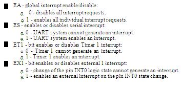
42 7. Discuss about the organization of internal RAM & Special Function Registers of 8051 microcontroller. (AUC MAY 2011) Same as Q1 8. Explain about the interrupt structure with the associated registers in 8051 microprocessor. (AUC MAY 2011) Interrupts An interrupt is a special feature which allows the 8051 to provide the illusion of "multitasking" although in reality the 8051 is only doing one thing at a time. The word "interrupt" can often be substituted with the word "event."an interrupt is triggered whenever a corresponding event occurs. When the event occurs, the 8051 temporarily puts "on hold" the normal execution of the program and executes a special section of code referred to as an interrupt handler. The interrupt handler performs whatever special functions are required to handle the event and then returns control to the 8051 at which point program execution continues as if it had never been interrupted. There are five interrupt sources for the 8051, which means that they can recognize 5 different events that can interrupt regular program execution. Each interrupt can be enabled or disabled by setting bits of the IE register. Likewise, the whole interrupt system can be disabled by clearing the EA bit of the same register. Refer to figure below. Now, it is necessary to explain a few details referring to external interrupts- INT0 and INT1. If the IT0 and IT1 bits of the TCON register are set, an interrupt will be generated on high to low transition, i.e. on the falling pulse edge (only in that moment). If these bits are cleared, an interrupt will be continuously executed as far as the pins are held low. EE2324/ Microprocessors & Microcontrollers Department of EEE 42
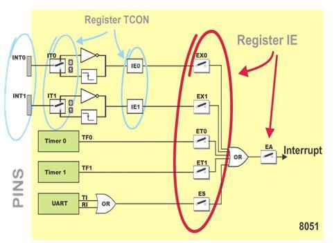

43 EE2324/ Microprocessors & Microcontrollers Department of EEE 43
 is written to the program counter in accordance to the table below: 4.")
44 Handling Interrupt When an interrupt request arrives the following occurs: 1. Instruction in progress is ended. 2. The address of the next instruction to execute is pushed on the stack. 3. Depending on which interrupt is requested, one of 5 vectors (addresses) is written to the program counter in accordance to the table below: 4. Interrupt Source Vector (Address) IE0 3h TF0 Bh TF1 1Bh RI, TI 23h 5. These addresses store appropriate subroutines processing interrupts. Instead of them, there are usually jump instructions specifying locations on which these subroutines reside. 6. When an interrupt routine is executed, the address of the next instruction to execute is poped from the stack to the program counter and interrupted program resumes operation from where it left off. From the moment the interrupt is enabled, the microcontroller is on alert all the time. When an interrupt request arrives, the program execution is stopped, the normal program execution is stopped & the control jumps to the appropriate address as shown in the table above. This address usually stores a jump instruction specifying the start of appropriate subroutine. After its execution the program resumes operation from where it left off. EE2324/ Microprocessors & Microcontrollers Department of EEE 44

45 Reset Reset occurs when the RS pin is supplied with a positive pulse in duration of at least 2 machine cycles (24 clock cycles of crystal oscillator). After that, the microcontroller generates an internal reset signal which clears all SFRs, except SBUF registers, Stack Pointer and ports (the state of the first two ports is not defined, while FF value is written to the ports configuring all their pins as inputs). Depending on surrounding and purpose of device, the RS pin is usually connected to a power-on reset push button or circuit or to both of them. Figure below illustrates one of the simplest circuit providing safe power-on reset. Basically, everything is very simple: after turning the power on, electrical capacitor is being charged for several milliseconds through a resistor connected to the ground. The pin is driven high during this process. When the capacitor is charged, power supply voltage is already stable and the pin remains connected to the ground, thus providing normal operation of the microcontroller. Pressing the reset button causes the capacitor to be temporarily discharged and the microcontroller is reset. When released, the whole process is repeated Through the program- step by step... Microcontrollers normally operate at very high speed. The use of 12 Mhz quartz crystal enables instructions to be executed per second. Basically, there is no need for higher operating rate. In case it is needed, it is easy to built in a crystal for high frequency. The problem arises when it is necessary to slow down the operation of the microcontroller. For example during testing in real environment when it is necessary to execute several instructions step by step in order to check EE2324/ Microprocessors & Microcontrollers Department of EEE 45

46 I/O pins' logic state. Interrupt system of the 8051 microcontroller practically stops operation of the microcontroller and enables instructions to be executed one after another by pressing the button. Two interrupt features enable that: Interrupt request is ignored if an interrupt of the same priority level is in progress. Upon interrupt routine execution, a new interrupt is not executed until at least one instruction from the main program is executed. In order to use this in practice, the following steps should be done: 1. External interrupt sensitive to the signal level should be enabled (for example INT0). 2. Three following instructions should be inserted into the program (at the 03hex. address): What is going on? As soon as the P3.2 pin is cleared (for example, by pressing the button), the microcontroller will stop program execution and jump to the 03hex address will be executed. This address stores a short interrupt routine consisting of 3 instructions. The first instruction is executed until the push button is realized (logic one (1) on the P3.2 pin). The second instruction is executed until the push button is pressed again. Immediately after that, the RETI instruction is executed and the processor resumes operation of the main program. Upon execution of any program instruction, the interrupt INT0 is generated and the whole procedure is repeated (push button is still pressed). In other words, one button press - one instruction. EE2324/ Microprocessors & Microcontrollers Department of EEE 46
e-pg Pathshala Subject : Computer Science Paper: Embedded System Module: 8051 Architecture Module No: CS/ES/5 Quadrant 1 e-text
 e-pg Pathshala Subject : Computer Science Paper: Embedded System Module: 8051 Architecture Module No: CS/ES/5 Quadrant 1 e-text In this lecture the detailed architecture of 8051 controller, register bank,
Memory Organization. Program Memory
 Memory Organization The 8051 has two types of memory and these are Program Memory and Data Memory. Program Memory (ROM) is used to permanently save the program being executed, while Data Memory (RAM) is
UNIT 5. Microcontrollers. Syllabus
 UNIT 5 Microcontrollers Syllabus Architecture of 8051 Signals Operational features Memory and I/O addressing Interrupts Instruction set Applications. OVERVIEW The past three decades have seen the introduction
8051 Microcontroller
 8051 Microcontroller 1 Salient Features (1). 8 bit microcontroller originally developed by Intel in 1980. (2). High-performance CMOS Technology. (3). Contains Total 40 pins. (4). Address bus is of 16 bit
Memory organization Programming model - Program status word - register banks - Addressing modes - instruction set Programming examples.
 MICROCONTROLLERS AND APPLICATIONS 1 Module 2 Module-2 Contents: Memory organization Programming model - Program status word - register banks - Addressing modes - instruction set Programming examples. MEMORY
8051 Microcontroller. Ali Ziya Alkar 1
 8051 Microcontroller Ali Ziya Alkar 1 8051 Introduction 8051 is one of the most popular microcontrollers in use today. Many derivative microcontrollers have since been developed that are based on--and
THE 8051 MICROCONTROLLER Simple comparison: Pentium vs. 8051
 THE 8051 MICROCONTROLLER Simple comparison: Pentium vs. 8051 FEATURE 8051 PENTIUM COMMENT Clock Speed 12Mhz. typical 1,000 MHz. (1GHz.) but 60MHz. ICs available 8051 internally divides clock by 12 so for
EEE3410 Microcontroller Applications Department of Electrical Engineering Lecture 4 The 8051 Architecture
 Department of Electrical Engineering Lecture 4 The 8051 Architecture 1 In this Lecture Overview General physical & operational features Block diagram Pin assignments Logic symbol Hardware description Pin
Module I. Microcontroller can be classified on the basis of their bits processed like 8bit MC, 16bit MC.
 MICROCONTROLLERS AND APPLICATIONS 1 Module 1 Module I Introduction to Microcontrollers: Comparison with Microprocessors Harvard and Von Neumann Architectures - 80C51 microcontroller features - internal
8051 MICROCONTROLLER
 8051 MICROCONTROLLER Mr.Darshan Patel M.Tech (Power Electronics & Drives) Assistant Professor Department of Electrical Engineering Sankalchand Patel College of Engineering-Visnagar WHY DO WE NEED TO LEARN
8051 Microcontroller
 8051 Microcontroller The 8051, Motorola and PIC families are the 3 leading sellers in the microcontroller market. The 8051 microcontroller was originally developed by Intel in the late 1970 s. Today many
8051 Microcontrollers
 8051 Microcontrollers Richa Upadhyay Prabhu NMIMS s MPSTME richa.upadhyay@nmims.edu March 8, 2016 Controller vs Processor Controller vs Processor Introduction to 8051 Micro-controller In 1981,Intel corporation
 8051 Memory Organization BY D. BALAKRISHNA, Research Assistant, IIIT-H Chapter 1: Memory Organization There are 2 types of memories available in 8051 microcontroller. Program memory/c code memory (ROM)
Three criteria in Choosing a Microcontroller
 The 8051 Microcontroller architecture Contents: Introduction Block Diagram and Pin Description of the 8051 Registers Some Simple Instructions Structure of Assembly language and Running an 8051 program
8-bit Microcontroller with 8K Bytes In-System Programmable Flash AT89S52
 Features Compatible with MCS -51 Products 8K Bytes of In-System Programmable (ISP) Flash Memory Endurance: 10,000 Write/Erase Cycles 4.0V to 5.5V Operating Range Fully Static Operation: 0 Hz to 33 MHz
MICROPROCESSORS AND MICROCONTROLLERS MATERIAL. Features of 8051:
 DEPARTMENT OF ECE MICROPROCESSORS AND MICROCONTROLLERS MATERIAL UNIT V 8051 MICROCONTROLLERS To make a complete microcomputer system, only microprocessor is not sufficient. It is necessary to add other
EE6502- MICROPROCESSOR AND MICROCONTROLLER
 . EE6502- MICROPROCESSOR AND MICROCONTROLLER UNIT III - 8051 MICROCONTROLLER PART - A 1. What is Microcontroller? A device which contains the microprocessor with integrated peripherals like memory, serial
MODULE-1. Short Answer Questions
 MODULE-1 Short Answer Questions 1. Give the comparison between microprocessor and microcontroller. It is very clear from figure that in microprocessor we have to interface additional circuitry for providing
8051 microcontrollers
 8051 microcontrollers Presented by: Deepak Kumar Rout Synergy Institute of Engineering and Technology, Dhenkanal Chapter 2 Introduction Intel MCS-51 family of microcontrollers consists of various devices
The Microcontroller. Lecture Set 3. Major Microcontroller Families. Example Microcontroller Families Cont. Example Microcontroller Families
 The Microcontroller Lecture Set 3 Architecture of the 8051 Microcontroller Microcontrollers can be considered as self-contained systems with a processor, memory and I/O ports. In most cases, all that is
Introduction To MCS-51
 Introduction To MCS-51 By Charoen Vongchumyen Department of Computer Engineering Faculty of Engineering KMITLadkrabang 8051 Hardware Basic Content Overview Architechture Memory map Register Interrupt Timer/Counter
MICROCONTROLLER AND PLC LAB-436 SEMESTER-5
 MICROCONTROLLER AND PLC LAB-436 SEMESTER-5 Exp:1 STUDY OF MICROCONTROLLER 8051 To study the microcontroller and familiarize the 8051microcontroller kit Theory:- A Microcontroller consists of a powerful
MICROPROCESSOR & MICROCONTROLLER
 a) From road north to East From road east to north From road south to west From road west to south From road west to north b) From road north to East From road south to west From road south to north From
CS 320. Computer Architecture Core Architecture
 CS 320 Computer Architecture 8051 Core Architecture Evan Hallam 19 April 2006 Abstract The 8051 is an 8-bit microprocessor designed originally in the 1980 s by the Intel Corporation. This inexpensive and
Microcontrollers. Fig. 1 gives a comparison of a microprocessor system and a microcontroller system.
 Syllabus: : Introduction to, 8051 Microcontroller Architecture and an example of Microcontroller based stepper motor control system (only Block Diagram approach). (5 Hours) Introduction to A microcontroller
Understanding the basic building blocks of a microcontroller device in general. Knows the terminologies like embedded and external memory devices,
 Understanding the basic building blocks of a microcontroller device in general. Knows the terminologies like embedded and external memory devices, CISC and RISC processors etc. Knows the architecture and
8051 MICROCONTROLLER
 What is a Microcontroller? UNIT 5 8051 MICROCONTROLLER A Microcontroller is a programmable digital processor with necessary peripherals. Both microcontrollers and microprocessors are complex sequential
8051 Overview and Instruction Set
 8051 Overview and Instruction Set Curtis A. Nelson Engr 355 1 Microprocessors vs. Microcontrollers Microprocessors are single-chip CPUs used in microcomputers Microcontrollers and microprocessors are different
MAHALAKSHMI ENGINEERING COLLEGE TIRUCHIRAPALLI UNIT- IV
 UNIT- IV PART A (2 MARK QUESTIONS) 1. What is the need for de-bouncing the keyboard? (AUC NOV 2012) Debouncing is any kind of hardware device or software that ensures that only a single signal will be
UNIT IV MICROCONTROLLER
 UNIT IV 8051- MICROCONTROLLER Prepared by R. Kavitha Page 1 Application Prepared by R. Kavitha Page 2 Pin Description of the 8051 UNIT IV- 8051 MICROCONTROLLER P1.0 P1.1 P1.2 P1.3 P1.4 P1.5 P1.6 P1.7 RST
Serial I-O for Dinesh K. Sharma Electrical Engineering Department I.I.T. Bombay Mumbai (version 14/10/07)
") Serial I-O for 8051 Dinesh K. Sharma Electrical Engineering Department I.I.T. Bombay Mumbai 400 076 (version 14/10/07) 1 Motivation Serial communications means sending data a single bit at a time. But
Serial I-O for 8051 Dinesh K. Sharma Electrical Engineering Department I.I.T. Bombay Mumbai 400 076 (version 14/10/07) 1 Motivation Serial communications means sending data a single bit at a time. But
CPEG300 Embedded System Design. Lecture 3 Memory
 CPEG300 Embedded System Design Lecture 3 Memory Hamad Bin Khalifa University, Spring 2018 Review Von Neumann vs. Harvard architecture? System on Board, system on chip? Generic Hardware Architecture of
Question Bank Microprocessor and Microcontroller
 QUESTION BANK - 2 PART A 1. What is cycle stealing? (K1-CO3) During any given bus cycle, one of the system components connected to the system bus is given control of the bus. This component is said to
8051 Microcontroller
 8051 Microcontroller EE4380 Fall 2001 Pari vallal Kannan Center for Integrated Circuits and Systems University of Texas at Dallas 8051 Architecture Programmer s View Register Set Instruction Set Memory
ENE 334 Microprocessors
 Page 1 ENE 334 Microprocessors Lecture 7: MCS-51 Architecture I : Dejwoot KHAWPARISUTH http://webstaff.kmutt.ac.th/~dejwoot.kha/ ENE 334 MCS-51 Architecture I Page 2 Outlines: 8051 Microcontroller Hardware
80C51 Block Diagram. CSE Overview 1
 80C51 Block Diagram CSE 477 8051 Overview 1 80C51 Memory CSE 477 8051 Overview 3 8051 Memory The data width is 8 bits Registers are 8 bits Addresses are 8 bits i.e. addresses for only 256 bytes! PC is
3. (a) Explain the steps involved in the Interfacing of an I/O device (b) Explain various methods of interfacing of I/O devices.
 Explain the steps involved in the Interfacing of an I/O device (b) Explain various methods of interfacing of I/O devices.") Code No: R05320202 Set No. 1 1. (a) Discuss the minimum mode memory control signals of 8086? (b) Explain the write cycle operation of the microprocessor with a neat timing diagram in maximum mode. [8+8]
Code No: R05320202 Set No. 1 1. (a) Discuss the minimum mode memory control signals of 8086? (b) Explain the write cycle operation of the microprocessor with a neat timing diagram in maximum mode. [8+8]
Architecture & Instruction set of 8085 Microprocessor and 8051 Micro Controller
 of 8085 microprocessor 8085 is pronounced as "eighty-eighty-five" microprocessor. It is an 8-bit microprocessor designed by Intel in 1977 using NMOS technology. It has the following configuration 8-bit
Microcontroller and Embedded Systems:
 Microcontroller and Embedded Systems: Branches: 1. Electronics & Telecommunication Engineering 2. Electrical & Electronics Engineering Semester: 6 th Semester / 7 th Semester 1. Explain the differences
CHAPTER ASSEMBLY LANGUAGE PROGRAMMING
 CHAPTER 2 8051 ASSEMBLY LANGUAGE PROGRAMMING Registers Register are used to store information temporarily: A byte of data to be processed An address pointing to the data to be fetched The vast majority
UNIT V MICRO CONTROLLER PROGRAMMING & APPLICATIONS TWO MARKS. 3.Give any two differences between microprocessor and micro controller.
 UNIT V -8051 MICRO CONTROLLER PROGRAMMING & APPLICATIONS TWO MARKS 1. What is micro controller? Micro controller is a microprocessor with limited number of RAM, ROM, I/O ports and timer on a single chip
Introducing The MCS 251 Microcontroller -- 8XC251SB
 E AP- 708 APPLICATION NOTE Introducing The MCS 251 Microcontroller -- 8XC251SB YONG-YAP SOH TECHNICAL MARKETING EIGHT-BIT MICROCONTROLLERS February 1995 Order Number: 272670-001 Intel Corporation makes
Lecture 1. Course Overview and The 8051 Architecture
 Lecture 1 Course Overview and The 8051 Architecture MCUniversity Program Lectures 8051 architecture t System overview of C8051F020 8051 instruction set System clock, crossbar and GPIO Assembler directives
EXPERIMENT NO.1. A Microcontroller is a complete computer system built on a single chip.
 EXPERIMENT NO.1 AIM: Study of 8051 Microcontroller TOOLS: 8051 kit THEORY: Salient Features of 8051 A Microcontroller is a complete computer system built on a single chip. It contains all components like
UNIT MICROCONTROLLER AND ITS PROGRAMMING
 M i c r o p r o c e s s o r s a n d M i c r o c o n t r o l l e r s P a g e 1 UNIT-7 8051 MICROCONTROLLER AND ITS PROGRAMMING INTRODUCTION The microcontroller incorporates all the features that are found
 Distributed by: www.jameco.com 1-800-831-4242 The content and copyrights of the attached material are the property of its owner. 8051 8052 and 80C51 Hardware Description December 1992 Order Number 270252-006
MODEL ANSWER SUBJECT- MICROCONTROLLER(12187) CLASS-EJ5E CLASS TEST-02 Q1.)Attempt any THREE of the following.
 CLASS-EJ5E CLASS TEST-02 Q1.)Attempt any THREE of the following.") MODEL ANSWER SUBJECT- MICROCONTROLLER(12187) CLASS-EJ5E CLASS TEST-02 Q1.)Attempt any THREE of the following. (9M) 1) Describe the instructions SWAP A and MOVX@DPTR,A with one example. (3Marks) SWAP A
MODEL ANSWER SUBJECT- MICROCONTROLLER(12187) CLASS-EJ5E CLASS TEST-02 Q1.)Attempt any THREE of the following. (9M) 1) Describe the instructions SWAP A and MOVX@DPTR,A with one example. (3Marks) SWAP A
Rev. No. History Issue Date Remark
 Preliminary Bar Code Reader Document Title Bar Code Reader Revision History Rev. No. History Issue Date Remark 0.0 Initial issue June 5, 2000 Preliminary 0.1 Change document title from Bar Code Reader
CHAPTER 5 : Introduction to Intel 8085 Microprocessor Hardware BENG 2223 MICROPROCESSOR TECHNOLOGY
 CHAPTER 5 : Introduction to Intel 8085 Hardware BENG 2223 MICROPROCESSOR TECHNOLOGY The 8085A(commonly known as the 8085) : Was first introduced in March 1976 is an 8-bit microprocessor with 16-bit address
SANKALCHAND PATEL COLLEGE OF ENGINEERING, VISNAGAR. ELECTRONICS & COMMUNICATION DEPARTMENT Question Bank- 1
 SANKALCHAND PATEL COLLEGE OF ENGINEERING, VISNAGAR ELECTRONICS & COMMUNICATION DEPARTMENT Question Bank- 1 Subject: Microcontroller and Interfacing (151001) Class: B.E.Sem V (EC-I & II) Q-1 Explain RISC
Architecture and Programming of 8051 Microcontrollers
 Architecture and Programming of 8051 Microcontrollers Learn in a quick and easy way to program 8051 microcontroller using many practical examples we have provided for you. Despite its relative old age,
8051 Core Specification
 8051 Core Specification Authors: Jaka Simsic Simon Teran jakas@opencores.org simont@opencores.org Rev. 0.1 August 14, 2001 First Draft www.opencores.org Rev 0.1 First Draft 1 of 26 Revision History Rev.
ISSI. IS89C51 CMOS SINGLE CHIP 8-BIT MICROCONTROLLER with 4-Kbytes of FLASH ISSI IS89C51 NOVEMBER 1998 FEATURES GENERAL DESCRIPTION
 IS89C51 CMOS SINGLE CHIP 8-BIT MICROCONTROLLER with 4-Kbytes of FLASH NOVEMBER 1998 FEATURES 80C51 based architecture 4-Kbytes of on-chip Reprogrammable Flash Memory 128 x 8 RAM Two 16-bit Timer/Counters
SOLUTION MANUAL FOR THE 8051 MICROCONTROLLER 4TH EDITION BY MACKENZIE AND PHAN
 SOLUTION MANUAL FOR THE 8051 MICROCONTROLLER 4TH EDITION BY MACKENZIE AND PHAN Chapter 1 - Introduction to Microcontrollers 1. (a)the first widely used microprocessor was the 8080. (b) The 8080 was introduced
8051 Timers and Serial Port
 8051 Timers and Serial Port EE4380 Fall 2001 Class 10 Pari vallal Kannan Center for Integrated Circuits and Systems University of Texas at Dallas Timer: Mode 1 Operation (recap) 16 bit counter. Load the
MCS-51 Serial Port A T 8 9 C 5 2 1
 MCS-51 Serial Port AT89C52 1 Introduction to Serial Communications Serial vs. Parallel transfer of data Simplex, Duplex and half-duplex modes Synchronous, Asynchronous UART Universal Asynchronous Receiver/Transmitter.
MSM80C154S MSM83C154S MSM85C154HVS USER'S MANUAL
 MSM8C54S MSM83C54S MSM85C54HVS USER'S MANUAL Copyright 988, OKI ELECTRIC INDUSTRY COMPANY, LTD. OKI makes no warranty for the use of its products and assumes no responsibility for any errors which may
UNIT-III ASSEMBLY LANGUAGE PROGRAMMING. The CPU can access data in various ways, which are called addressing modes
 8051 Software Overview: 1. Addressing Modes 2. Instruction Set 3. Programming 8051 Addressing Modes: UNIT-III ASSEMBLY LANGUAGE PROGRAMMING The CPU can access data in various ways, which are called addressing
1. INTRODUCTION TO MICROPROCESSOR AND MICROCOMPUTER ARCHITECTURE:
 1. INTRODUCTION TO MICROPROCESSOR AND MICROCOMPUTER ARCHITECTURE: A microprocessor is a programmable electronics chip that has computing and decision making capabilities similar to central processing unit
8051 Microcontroller memory Organization and its Applications
 8051 Microcontroller memory Organization and its Applications Memory mapping in 8051 ROM memory map in 8051 family 0000H 4k 0000H 8k 0000H 32k 0FFFH DS5000-32 8051 1FFFH 8752 7FFFH from Atmel Corporation
Microcontroller Intel [Instruction Set]
![Microcontroller Intel [Instruction Set]](/thumbs/82/86620819.jpg "Microcontroller Intel [Instruction Set]") Microcontroller Intel 8051 [Instruction Set] Structure of Assembly Language [ label: ] mnemonic [operands] [ ;comment ] Example: MOV R1, #25H ; load data 25H into R1 2 8051 Assembly Language Registers
Microcontroller Intel 8051 [Instruction Set] Structure of Assembly Language [ label: ] mnemonic [operands] [ ;comment ] Example: MOV R1, #25H ; load data 25H into R1 2 8051 Assembly Language Registers
Department of EIE / Pondicherry Engineering College. Timer/Counters. Department of EIE / Pondicherry Engineering College 1
 Timer/Counters Department of EIE / Pondicherry Engineering College 1 The 8051 has two internal sixteen bit hardware Timer/Counters. Each Timer/Counter can be configured in various modes, typically based
8051 Microcontroller Interrupts
 8051 Microcontroller Interrupts There are five interrupt sources for the 8051, which means that they can recognize 5 different events that can interrupt regular program execution. Each interrupt can be
The Timers/Counters The Serial Interface The Interrupt System Reset P0.0-P0.7 P2.0-P2.7. Port 2 Drivers. Port 2 Latch
 HARDWARE DESCRIPTION This chapter provides a detailed description of the 80C51 microcontroller (see Figure 1). Included in this description are: The port drivers and how they function both as ports and,
Module Contents of the Module Hours COs
 Microcontrollers (EE45): Syllabus: Module Contents of the Module Hours COs 1 8051 MICROCONTROLLER ARCHITECTURE: Introduction to Microprocessors and Microcontrollers, the 8051 Architecture, 08 1 and pin
TUTORIAL. Donal Heffernan University of Limerick May Tutorial D.Heffernan 2000,
 8051 TUTORIAL Donal Heffernan University of Limerick May-2002 8051 Tutorial D.Heffernan 2000, 2001 1 Blank 8051 Tutorial D.Heffernan 2000, 2001 2 Some reference material: Test books + MacKenzie Scott.
CPEG300 Embedded System Design. Lecture 6 Interrupt System
 CPEG300 Embedded System Design Lecture 6 Interrupt System Hamad Bin Khalifa University, Spring 2018 Correction Lecture 3, page 18: Only direct addressing mode is allowed for pushing or popping the stack:
8051 Microcontrollers
 8051 Microcontrollers Author: Milan Verle compilation with Meisam Fanoody 1 Chapter 1: Introduction to Microcontrollers Chapter 2: 8051 Microcontroller Architecture Chapter 3: The 8051 Instruction Set
 VALLIAMMAI ENGINEERING COLLEGE S.R.M. NAGAR, KATTANKULATHUR-603203. DEPARTMENT OF ELECTRICAL AND ELECTRONICS ENGINEERING VII-EEE EE6502- MICROPROCESSORS AND MICROCONTROLLERS QUESTION BANK UNIT I 1. What
8051 Serial Communication
 8051 Serial Communication Basics of serial communication Parallel: transfers eight bits of data simultaneously over eight data lines expensive - short distance fast Serial : one bit at a time is transferred
SYLLABUS UNIT - I 8086/8088 ARCHITECTURE AND INSTRUCTION SET
 1 SYLLABUS UNIT - I 8086/8088 ARCHITECTURE AND INSTRUCTION SET Intel 8086/8088 Architecture Segmented Memory, Minimum and Maximum Modes of Operation, Timing Diagram, Addressing Modes, Instruction Set,
Fig 1. Block diagram of a microcomputer
 MICRO CONTROLLERS www.bookspar.com VTU NOTES QUESTION PAPERS UNIT - 1 Computer: A computer is a multipurpose programmable machine that reads binary instructions from its memory, accepts binary data as
Moodle WILLINGDON COLLEGE SANGLI (B. SC.-II) Digital Electronics
 Digital Electronics") Moodle 4 WILLINGDON COLLEGE SANGLI (B. SC.-II) Digital Electronics Advanced Microprocessors and Introduction to Microcontroller Moodle developed By Dr. S. R. Kumbhar Department of Electronics Willingdon
Moodle 4 WILLINGDON COLLEGE SANGLI (B. SC.-II) Digital Electronics Advanced Microprocessors and Introduction to Microcontroller Moodle developed By Dr. S. R. Kumbhar Department of Electronics Willingdon
Handshake Solutions. HT80C51 User Manual
 HT8C5 User Manual HT8C5 User Manual Document Information Document Information Document Title Date of Creation 27/6/25 Date of last change 27/6/25 File name Status Version Number.7 Client / Target Audience
Department of Electronics and Instrumentation Engineering Question Bank
 www.examquestionpaper.in Department of Electronics and Instrumentation Engineering Question Bank SUBJECT CODE / NAME: ET7102 / MICROCONTROLLER BASED SYSTEM DESIGN BRANCH : M.E. (C&I) YEAR / SEM : I / I
Microcontrollers can be considered as self-contained systems with a processor, memory and I/O ports.
 8051 Architecture 1 Microcontrollers can be considered as self-contained systems with a processor, memory and I/O ports. In most cases, all that is missing is the software to define the operation of the
Architecture of 8085 microprocessor
 Architecture of 8085 microprocessor 8085 consists of various units and each unit performs its own functions. The various units of a microprocessor are listed below Accumulator Arithmetic and logic Unit
_ V Intel 8085 Family In-Circuit Emulation. Contents. Technical Notes
 _ V9.12. 225 Technical Notes Intel 8085 Family In-Circuit Emulation This document is intended to be used together with the CPU reference manual provided by the silicon vendor. This document assumes knowledge
Embedded World Television, Radio, CD player, Washing Machine Microwave Oven Card readers, Palm devices
 A presentation on INTRODUCTION We are living in the Embedded World. We are surrounded with many embedded products and our daily life largely depends on the proper functioning of these gadgets. Television,
2. List the five interrupt pins available in INTR, TRAP, RST 7.5, RST 6.5, RST 5.5.
 DHANALAKSHMI COLLEGE OF ENGINEERING DEPARTMENT OF ELECTRICAL AND ELECTRONICS ENGINEERING EE6502- MICROPROCESSORS AND MICROCONTROLLERS UNIT I: 8085 PROCESSOR PART A 1. What is the need for ALE signal in
Module 3. Embedded Systems I/O. Version 2 EE IIT, Kharagpur 1
 Module 3 Embedded Systems I/O Version 2 EE IIT, Kharagpur 1 Lesson 15 Interrupts Version 2 EE IIT, Kharagpur 2 Instructional Objectives After going through this lesson the student would learn Interrupts
8XC51RA RB RC Hardware Description
 8XC51RA RB RC Hardware Description February 1995 Order Number 272668-001 Information in this document is provided in connection with Intel products Intel assumes no liability whatsoever including infringement
C51 Family. Architectural Overview of the C51 Family. Summary
 Architectural Overview of the C51 Family C51 Family Summary 1. Introduction............................................................ I.1. 1.1. TSC80C51/80C51/80C31.................................................................
SN8F5000 Family Instruction Set
 SONiX Technology Co., Ltd. 8051-based Microcontroller 1 Overview SN8F5000 is 8051 Flash Type microcontroller supports comprehensive assembly instructions and which are fully compatible with standard 8051.
ELEG3923 Microprocessor Ch.10 Serial Port Programming
 Department of Electrical Engineering University of Arkansas ELEG3923 Microprocessor Ch.10 Serial Port Programming Dr. Jingxian Wu wuj@uark.edu OUTLINE 2 Basics of Serial Communication Serial port programming
Description of the Simulator
 Description of the Simulator The simulator includes a small sub-set of the full instruction set normally found with this style of processor. It includes advanced instructions such as CALL, RET, INT and
Embedded Controller Programming
 Embedded Controller Programming Counters, Timers and I/O in Assembly Language Ken Arnold Copyright 2000-2004 Ken Arnold 1 Outline Timer/Counters Serial Port More 8051 Instructions Examples Copyright 2000-2004
Embedded Systems Lab Lab 1 Introduction to Microcontrollers Eng. Dalia A. Awad
 Embedded Systems Lab Lab 1 Introduction to Microcontrollers Eng. Dalia A. Awad Objectives To be familiar with microcontrollers, PIC18F4550 microcontroller. Tools PIC18F4550 Microcontroller, MPLAB software,
Control Unit: The control unit provides the necessary timing and control Microprocessor resembles a CPU exactly.
 Unit I 8085 and 8086 PROCESSOR Introduction to microprocessor A microprocessor is a clock-driven semiconductor device consisting of electronic logic circuits manufactured by using either a large-scale
b. List different system buses of 8085 microprocessor and give function of each bus. (8) Answer:
 Answer:") Q.2 a. Discuss and differentiate between a Microprocessor and a Microcontroller. Microprocessor is an IC which has only the CPU inside them i.e. only the processing powers such as Intel s Pentium 1,2,3,4,
Q.2 a. Discuss and differentiate between a Microprocessor and a Microcontroller. Microprocessor is an IC which has only the CPU inside them i.e. only the processing powers such as Intel s Pentium 1,2,3,4,
Principle and Interface Techniques of Microcontroller
 Principle and Interface Techniques of Microcontroller --8051 Microcontroller and Embedded Systems Using Assembly and C LI, Guang ( 李光 ) Prof. PhD, DIC, MIET WANG, You ( 王酉 ) PhD, MIET 杭州 浙江大学 2014 Chapter
QUESTION BANK CS2252 MICROPROCESSOR AND MICROCONTROLLERS
 FATIMA MICHAEL COLLEGE OF ENGINEERING & TECHNOLOGY Senkottai Village, Madurai Sivagangai Main Road, Madurai -625 020 QUESTION BANK CS2252 MICROPROCESSOR AND MICROCONTROLLERS UNIT 1 - THE 8085 AND 8086
Chapter 9. Programming Framework
 Chapter 9 Programming Framework Lesson 1 Registers Registers Pointers Accumulator Status General Purpose Outline CPU Registers Examples 8-bitA (Accumulator) Register 8-bit B Register 8-bitPSW (Processor
MICROCONTROLLER UNIT 1
 MICROCONTROLLER UNIT 1 OUTLINE INTRODUCTION MICROCONTROLLERS AND EMBEDDED PROCESSORS OVERVIEW OF THE 8051 8051 MICTROCONTROLLER HARDWARE ADDRESSING MODES INTRODUCTION The first task to use a new computer
8051 Peripherals. On-Chip Memory Timers Serial Port Interrupts. Computer Engineering Timers
 8051 Peripherals On-Chip Memory Timers Serial Port Interrupts Computer Engineering 2 2-1 8051 Timers 8051 Timers The 8051 has 2 internal 16-bit timers named Timer 0 and Timer 1 Each timer is a 16-bit counter
Chapter Operation Pinout Operation 35
 68000 Operation 35 Chapter 6 68000 Operation 6-1. 68000 Pinout We will do no construction in this chapter; instead, we will take a detailed look at the individual pins of the 68000 and what they do. Fig.
ENE 334 Microprocessors
 Page 1 ENE 334 Microprocessors Lecture 9: MCS-51: Moving Data : Dejwoot KHAWPARISUTH http://webstaff.kmutt.ac.th/~dejwoot.kha/ ENE 334 MCS-51 Moving Data Page 2 Moving Data: Objectives Use commands that
UNIT 2 THE 8051 INSTRUCTION SET AND PROGRAMMING
 UNIT 2 THE 8051 INSTRUCTION SET AND PROGRAMMING Instructions Alphabetical List of Instructions ACALL: Absolute Call ADD, ADDC: Add Accumulator (With Carry) AJMP: Absolute Jump ANL: Bitwise AND CJNE: Compare
ELEG3924 Microprocessor
 Department of Electrical Engineering University of Arkansas ELEG3924 Microprocessor Ch.2 Assembly Language Programming Dr. Jing Yang jingyang@uark.edu 1 OUTLINE Inside 8051 Introduction to assembly programming
ENE 334 Microprocessors
 Page 1 ENE 334 Microprocessors Lecture 10: MCS-51: Logical and Arithmetic : Dejwoot KHAWPARISUTH http://webstaff.kmutt.ac.th/~dejwoot.kha/ ENE 334 MCS-51 Logical & Arithmetic Page 2 Logical: Objectives