Understanding the basic building blocks of a microcontroller device in general. Knows the terminologies like embedded and external memory devices,
|
|
|
- Gloria Logan
- 6 years ago
- Views:
Transcription
1 Understanding the basic building blocks of a microcontroller device in general. Knows the terminologies like embedded and external memory devices, CISC and RISC processors etc. Knows the architecture and silent features of 8051 microcontrollers. Knows the architecture of Intel bit microcontroller. Knows about configuring the 8096

2 Microcontroller Contents Introduction Inside 8051 Instructions Interfacing Introduction Definition of a Microcontroller Difference with a Microprocessor Microcontroller is used where ever Definition It is a single chip Consists of Cpu, Memory I/O ports, timers and other peripherals
3 Where ever Small size Low cost Low power Architecture Harvard university The Architecture given by Harvard University has the following advantages: 1: Data Space and Program Space are distinct 2: There is no Data corruption or loss of data Disadvantage is: 1: The circuitry is very complex. Features 8 bit cpu 64k Program memory (4k on chip) 64k Data memory 128 Bytes on chip 32 I/O Two 16 bit timers Full duplex UART 6 Source/5 Vector interrupts with two level priority levels On chip clock Oscillator.
4 Block Diagram
5 Memory Architecture
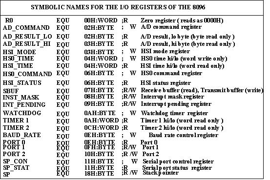
6 SFR Map
7 Internal Memory

8 Pin connections Overview of bit microcontroller Features 232 Byte Register File. Register to Register Architecture. 10 bit A/D Converter with S/H. Five 8 bit I/O ports. 20 Interrupt Sources. Pulse Width Modulation Output. High speed I/O subsystem. Dedicated Baud Rate Generator. Full Duplex Serial Port. 16 bit Watchdog Timer. Introduction The MSC-96 family members are all high performance microcontroller with a 16 bit CPU and atleast 230 bytes of on-chip RAM. Intel MSC-96 family easily handles high speed calculations and fast input/out operations. All of the MCS-96 components share a common instruction set and architecture.
9 However the CHMOS components have enhancements to provide higher performance with lower power consumption. These microcontroller contains dedicated I/O subsystem and perform 16-bit arithmetic instructions including multiply and divide operations. CPU :The major components of the MCS-96 CPU are the Register File and the Register / Arithmetic Logic Unit (RALU). Location 00H through 17H are the I/O control registers or Special function registers (SFR). Locations 18H and 19H contains the stack pointer, which can serve as general purpose RAM when not performing stack operations. The remaining bytes of the register file serve as general purpose RAM, accessible as bytes, words or double-words. Calculations performed by the CPU take place in the RALU. The RALU contains a 17bit ALU, the program status word (PSW), the program Counter (PC), a loop counter and three temporary registers. The RALU operates directly on the Register Files, thus eliminating accumulator bottleneck and providing for direct control of I/O operations through the SFR. Architecture The MCS-96 supports a complete instruction set which includes bit operations, byte operations, word operations, double-word operations (unsigned 32 bit), long operations (signed 32 bit), flag manipulations as well as jump and call instructions. All the standard logical and arithmetic instructions function as both byte and word operations. The jump bit set and jump bit clear instructions can operate on any of the SFR or bytes in the lower register files. These fast bit manipulations allow for rapid I/O functions. Byte and word operations make up the instruction set. The assembly language ASM-96 uses a B suffix on a mnemonic for a byte operation or for word operation. Addressing modes: This supports the following modes. Register-direct, indirect, indirect with auto-increment, immediate, short-indexed and long-indexed. These modes increase the flexibility and overall execution speed of the MCS-96 devices.
10
11
12 8096 Peripherals Standard I/O Ports The 8096 has five 8 bit I/O ports. Port 0 is an input port that is also the analog input for the A/D converter. Port 1 is a quasi-bidirectional port. Port 2 contains three types of port lines. Quasi-Bidirectional, input and output. Other functions on the 8096 share the input and output lines with Port 2. Port 3 and 4 are open-drain bidirectional ports that share their pins with the address/data bus. Timers The 8096 has two 16 bit timers. Timer 1 and Timer 2. An internal clock increments the Timer 1 value every 8 state times. ( A state time is 3 oscillator periods) An external clock increments Timer 2 on every positive and negative transition. Either an internal or external source can reset Timer 2. This two timers can generate an interrupt when crossing the 0FFFFH/0000H boundary. The 8096 includes separate, dedicated timers for serial port baud rate generator and watchdog timer. The watchdog Timer is an internal timer that resets the system if the software fails to operate properly. High Speed Input Unit (HSI) The 8096 HIS unit can record times of external events with a 9 state time resolution. It can monitor four independently configurable HSI lines and captures the value of timer 1 when events takes place. The four types of events that can trigger captures include: rising edge only, falling edge only, rising or falling edges, or every eight rising edge. The HSI unit can store upto 8 entries ( Timer 1 values ). Reading the HSI holding register unloads the earliest entry placed in the FIFO. The HSI unit can generate an interrupt when loading an entry into the HSI holding register or loading the sixth entry into the FIFO. High Speed Output Unit (HSO) The 8096 HSO unit can trigger events at specified times based on Timer1 or Timer2. These programmable events include: starting an A/D conversion, resetting Timer2, generating upto four software time delays, and setting or clearing one or more of the six HSO output lines. The HSO unit stores pending event and specified times in a Content Addressable Memory (CAM) file. This file stores upto 8 commands. Each command specifies the action time, the nature of the action, whether an interrupt is to occur, and whether Timer1 or Timer2 is the reference timer. Every 8 state times the HSO compares the CAM locations for time matches. The HSO unit triggers the specified event when it finds a time match. A command is cleared from the CAM as soon as it executes.
13 Serial Port The serial port on the 8096 has one synchronous (Mode 0) and three asynchronous modes (Modes 1, 2 and 3). The asynchronous modes are full duplex. Mode 0, the synchronous mode, is to expand the I/O capability of the 8096 using shift register. Mode 1 is the standard asynchronous mode used for normal serial communication. Modes 2, 3 are 9-bit modes commonly used for multiprocessor communications. Pulse Width Modulator (PWM) The PWM output waveform is a variable duty cycle pulse that repeats every 256 state times. The PWM output can perform digital to analog conversions and drive several types of motors that require a PWM waveform for more efficient operation. A/D Converter The 8096 A/D converts an analog input to a 10 bit digital equivalent. The main components of the A/D Converter are: 8 analog inputs, an 8 to 1 multiplexer, a sample and hold capacitor and resistor ladder. The A/D Converter can start a conversion immediately or the High Speed Output unit can trigger a conversion at a preprogrammed time. The A/D converter performs a conversion in 88 state times. Upon completion of each conversion the converter can generate a conversion complete interrupt. The 8X9X provides separate VREF and ANGND supply pins to isolate noise on the Vcc or Vss lines. Interrupts There are 21 interrupts sources and 8 interrupt vector on the When the interrupt controller detects one of the 8 interrupts it sets the corresponding bit in the interrupt pending register. Individual interrupts are enabled or disabled by setting or clearing bits in the interrupt mask register. When the interrupt controller decides to process an interrupt, it executes a call to an interrupt service routine ISR. The corresponding interrupt vector contains the address of the ISR. The interrupt controller then clears the associated pending bit.
14 Configuring the 8096 The 8096 can be operated in either the single-chip mode, or two of its ports can be redefined to bring out the internal address bus and data bus. For the single chip mode, the internal ROM and EPROM must be accessed. This choice is made by tying the EA# pin high. When EA pin is tied high, the internal ROM or EPROM is accessed during instruction and data fetches from addresses 2080 to 3FFFH and for interrupt vectors located at addresses 2000 to 2011H.
15
16
17 When operated in the expanded mode the internal ROM or EPROM can still be used by tying EA# high. Accesses to the addresses 2000 to 2011H and 2080 to 3FFFH can be made to access off-chip memory by tying the EA# pin low. If the EA pin is high, then we have the option of using the internal ROM or EPROM together with external memory and devices. One of the options made available by the BH series over the original 8096 family is the option to deal with either a 16 bit external data bus or else an 8 bit external data bus. The latter options permits expanding the 8096 with a single byte wide static RAM chip or with a single byte wide EPROM chip for program memory. The latter is particularly convenient for users who can either put their application program into a single EPROM or who do not have the EPROM programming capability to separate their object code into even addresses and odd addresses as required for the two byte wide EPROM used with a 16 bit data bus. The choice of bus width is made in two places. When the 8096 comes out of reset, it reads the content of address 2018H of our ROM or EPROM. This is called the chip configuration CCB. The 8096 stores this byte in a chip configuration register which is unaccessable by our software. Bit 1 works together with the external BUSWIDTH pin to determine the data bus width (when the EA pin is tied low). While the BUSWIDTH pin is tied either high or low, it can actually be changed during each bus cycle of normal operation. If it is tied to the A15 address lines, then accesses to external addresses 8000 to FFFFH would use a 16-bit data bus while accesses to external addresses below
18 this would use an 8-bit data bus. In either case, the full 16 bit address bus is brought out. When an 8-bit data bus is brought out, the lines which bring out the upper half of the address bus do not have to be multiplexed. In this case, the designers of the chip have saved users the need for an external latch for the upper half of the address bus by latching the address internally. The original 8096 parts gave the user of the expanded chip an ALE output. This was used to latch the address. The new option is selected with a 0 in bit 3 of CCB. The ADV# line remains high during any machine cycles which are not accessing external memory, but goes low during external accesses. Because of this ADV# can be used to simplify the decoding to enable external devices. In addition to the external access, ADV# drop low at precisely the current time to latch the multiplexed address. Consequently, it can serve double duty, both helping with decoding and also latching the multiplexed address. Another feature of the original 8096 parts operating in the expanded mode was the need to decode a BHE# signal. This was used during writes to a byte at an odd address so that the lower byte on the 16-bit data bus could be left unchanged. Users of the original 8096 parts had to gate BHE# together with a WR# signal to generate two write signals. One for chips connected to the upper half of the data bus and one for chip connected to the lower half of the data bus. This option is selected with 0 bit 2 of CCB. INST output is a signal which takes on when the RD# line is active, signaling that a read from an external device is taking place. If the read is an instruction fetch, then INST will be high. Otherwise it will be low during the read cycle. Users of logia analyzers and designers of 8096 emulators can use this signal to help sort out the activity on external bus. The READY control line permits the 8096 to run at full speed for its internal accesses and yet to slow down for some of its external accesses. It is used in conjunction with bits 4 and 5 of CCB to introduce extra 250ns ( assuming a 12 MHz crystal) wait states into external read and write cycles. If the READY line is tied high then the CCB bits do not matter and no external wait states are introduced into external read or writes. If the READY line is tied low( signifying that external devices are not ready), then this READY signal can be overridden by the CCB bits. Thus 00 in bits 4 and 5 of CCB will now limit the delay to a signal wait state. READY line can be changed by dynamically from cycle to cycle. If it is tied to the upper address lines, then we can position external devices which can run at full speed in the 8000 to FFFF address range and slower external device needing an extra wait state at lower addresses. The lock mode is selected by the coding of bit 6 and 7. whether the software is in on-chip manage to get the chip to execute code from external memory and then have that external program dump the internal memory to the serial port. In a read-protected mode, only code executing from internal memory can read from memory addresses between 2020 to 3FFFH.
19 In a write-protected mode, no code can write to memory address between 2000 and 3FFFH. One problem arises with a memory protection scheme such as, if we purchase ROM-protected parts from Intel, then before we use them, we would like to test them. We can drive the EA# line low and use our own program to test all the resource on the chip. This does not test the ROM contents. Intel supports the verification of ROM by including a 16byte security key, located at address 2020 to 202FH. Before protected memory can read, the chip must read external memory locations 4020 to 402FH and compare the contents with the internal security key. Access to protected memory will only be allowed if a match I found for all 16 bytes. The first 26 addresses from the register file, used to set up and access almost all of the on-chip resources. The rest of the page 0 is dedicated to internal RAM, for a total of 230 bytes of RAM. While the ROM or EPROM extends from 2000 to 3FFFH, Intel reserves addresses 2012 to 2017H.
20
21
22 General Purpose I/O Ports Port 0 whose lines can serve as either general purpose inputs or alternatively as input to the analog-to-digital converter family. Port 1 is a quasi-bidirectional I/O port. Port 2 includes four input lines, two output lines, and two quasi-bidirectional I/O lines. Port 3 and 4 when used as ports, they have open drain outputs. By writing anything but a 1 to a line, it can serve as an input even as other lines serve as an outputs. Each output line needs the addition of a pullup resistor having a value of 15kΩ. In the expanded mode the bus lines gain the ability to drive both high and low, forming the expansion bus without the need of pullup resistors.
23
24
25 1. The 8051 microcontroller is of pin package as a processor. a) 30, 1byte b) 20, 1 byte c) 40, 8 bit d) 40, 8 byte 2. The SP is of wide register. And this may be defined anywhere in the. a) 8 byte, on-chip 128 byte RAM. b) 8 bit, on chip 256 byte RAM. c) 16 bit, on-chip 128 byte ROM d) 8 bit, on chip 128 byte RAM.. 3. After reset, SP register is initialized to address. a) 8H b) 9H c) 7H d) 6H 4. What is the address range of SFR Register bank? a) 00H-77H b) 40H-80H c) 80H-7FH d) 80H-FFH 5. Which pin of port 3 is has an alternative function as write control signal for external data memory? a) P3.8 b) P3.3 c) P3.6 d) P What is the Address (SFR) for TCON, SCON, SBUF, PCON and PSW respectively? a) 88H, 98H, 99H, 87H, 0D0H. b) 98H, 99H, 87H, 88H, 0D0H c) 0D0H, 87H, 88H, 99H, 98H d) 87H, 88H, 0D0H, 98H, 99H 7. Match the following: 1) TCON i) contains status information 2) SBUF ii) timer / counter control register. 3) TMOD iii) idle bit, power down bit 4) PSW iv) serial data buffer for Tx and Rx. 5) PCON v) timer/ counter modes of operation. a) 1->ii, 2->iv, 3->v, 4->i, 5->iii. b) 1->i, 2->v, 3->iv, 4->iii, 5->ii. c) 1->v, 2->iii, 3->ii, 4->iv, 5->i. d) 1->iii, 2->ii, 3->i, 4->v, 5->iv. 8. Which of the following is of bit operations? i) SP ii) P2 iii) TMOD iv) SBUF v) IP a) ii, v only b) ii, iv, v only c) i, v only d) iii, ii only 9. Serial port interrupt is generated, if bits are set a) IE b) RI, IE c) IP, TI d) RI, TI 10. In 8051 which interrupt has highest priority? a)ie1 b)tf0 c)ie0 d)tf1
26 11. Intel 8096 is of bit microcontroller family called as. a) 8, MCS51 b) 16, MCS51 c) 8, MCS96 d) 16, MCS has following features fill up the following, i) Register file, ii) I/O Ports iii) architecture. a) 256 byte, five 8bit, register to register b) 256 byte, four 8bit, register to register c) 232 byte, five 8bit, register to register d) 232 byte, six 8 bit, register to register 13. How many synchronous and asynchronous modes are there in serial port of 8096? a) 2, 2 respectively b) 3,1 respectively c) 1, 3 respectively d) 1, 2 respectively 14. In 8096 we have interrupt sources and interrupt vectors. a) 18, 8 b) 21, 6 c) 21, 8 d) 16, has general purpose I/O ports, Port 2 includes of the following i) two quasi-bidirectional I/O lines ii) two output lines iii) four input lines iv) open drain outputs a) 4, i, iv b) 6, ii, iii c) 4, i,ii,iii d) 6, i, ii, iv write-protected mode, no code can write to memory address between. a) 2020 to 3FFFH b) 8000 to FFFFH c) 2000 to 3FFFH d) 2020 to 202FH 17. If the pin is, then we have the option of using the ROM or EPROM together with memory and devices. a) EA, high, internal, external b) EA, low, internal, external c) EA, high, external, internal d) EA, low, external, internal 18. In 8096, CCB bit 3 is. a) write strobe mode select b) address valid strobe select c) bus width select d) Internal read control mode 19. In 8096, mode of serial port are modes commonly used for communications. a) 1, 8bit, single processor b) 0, 7bit, multiple microcontroller c) 2, 9 bit, multiple processors d) 3, 8 bit, multiple microcontroller
27 20. What is the function of watchdog timer? a) The watchdog Timer is an external timer that resets the system if the software fails to operate properly. b) The watchdog Timer is an internal timer that sets the system if the software fails to operate properly. c) The watchdog Timer is an internal timer that resets the system if the software fails to operate properly. d) None of them Key: 5.1 C 5.2 D 5.3 C 5.4 D 5.5 C 5.6 A 5.7 A 5.8 A 5.9 D 5.10 C 5.11 D 5.12 C 5.13 C 5.14 C 5.15 C 5.16 C 5.17 A 5.18 B 5.19 C 5.20 C
CPU CPU MEMORY MICRO CONTROLLER MICRO PROCESSER. Consists Memory, I/o ports. Memory, I/O Ports to be connected externally. MEMORY I/O PORTS I/O PORTS
 Microcontroller Contents Introduction Inside 8051 Instructions Interfacing Introduction Definition of a Microcontroller Difference with a Microprocessor Microcontroller is used where ever Definition It
Features. M. Krishna Kumar MAM/M5/LU13/2004 1
 Features 232 Byte Register File. Register to Register Architecture. 10 bit A/D Converter with S/H. Five 8 bit I/O ports. 20 Interrupt Sources. Pulse Width Modulation Output. High speed I/O subsystem. Dedicated
8051 Microcontroller
 8051 Microcontroller The 8051, Motorola and PIC families are the 3 leading sellers in the microcontroller market. The 8051 microcontroller was originally developed by Intel in the late 1970 s. Today many
8051 Microcontroller
 8051 Microcontroller 1 Salient Features (1). 8 bit microcontroller originally developed by Intel in 1980. (2). High-performance CMOS Technology. (3). Contains Total 40 pins. (4). Address bus is of 16 bit
8-bit Microcontroller with 8K Bytes In-System Programmable Flash AT89S52
 Features Compatible with MCS -51 Products 8K Bytes of In-System Programmable (ISP) Flash Memory Endurance: 10,000 Write/Erase Cycles 4.0V to 5.5V Operating Range Fully Static Operation: 0 Hz to 33 MHz
UNIT IV MICROCONTROLLER
 UNIT IV 8051- MICROCONTROLLER Prepared by R. Kavitha Page 1 Application Prepared by R. Kavitha Page 2 Pin Description of the 8051 UNIT IV- 8051 MICROCONTROLLER P1.0 P1.1 P1.2 P1.3 P1.4 P1.5 P1.6 P1.7 RST
e-pg Pathshala Subject : Computer Science Paper: Embedded System Module: 8051 Architecture Module No: CS/ES/5 Quadrant 1 e-text
 e-pg Pathshala Subject : Computer Science Paper: Embedded System Module: 8051 Architecture Module No: CS/ES/5 Quadrant 1 e-text In this lecture the detailed architecture of 8051 controller, register bank,
Module 2. Embedded Processors and Memory. Version 2 EE IIT, Kharagpur 1
 Module 2 Embedded Processors and Memory Version 2 EE IIT, Kharagpur 1 Lesson 11 Embedded Processors - II Version 2 EE IIT, Kharagpur 2 Signals of a Typical Microcontroller In this lesson the student will
8051 microcontrollers
 8051 microcontrollers Presented by: Deepak Kumar Rout Synergy Institute of Engineering and Technology, Dhenkanal Chapter 2 Introduction Intel MCS-51 family of microcontrollers consists of various devices
MICROPROCESSORS AND MICROCONTROLLERS MATERIAL. Features of 8051:
 DEPARTMENT OF ECE MICROPROCESSORS AND MICROCONTROLLERS MATERIAL UNIT V 8051 MICROCONTROLLERS To make a complete microcomputer system, only microprocessor is not sufficient. It is necessary to add other
ENE 334 Microprocessors
 Page 1 ENE 334 Microprocessors Lecture 7: MCS-51 Architecture I : Dejwoot KHAWPARISUTH http://webstaff.kmutt.ac.th/~dejwoot.kha/ ENE 334 MCS-51 Architecture I Page 2 Outlines: 8051 Microcontroller Hardware
EEE3410 Microcontroller Applications Department of Electrical Engineering Lecture 4 The 8051 Architecture
 Department of Electrical Engineering Lecture 4 The 8051 Architecture 1 In this Lecture Overview General physical & operational features Block diagram Pin assignments Logic symbol Hardware description Pin
SYLLABUS UNIT - I 8086/8088 ARCHITECTURE AND INSTRUCTION SET
 1 SYLLABUS UNIT - I 8086/8088 ARCHITECTURE AND INSTRUCTION SET Intel 8086/8088 Architecture Segmented Memory, Minimum and Maximum Modes of Operation, Timing Diagram, Addressing Modes, Instruction Set,
CS 320. Computer Architecture Core Architecture
 CS 320 Computer Architecture 8051 Core Architecture Evan Hallam 19 April 2006 Abstract The 8051 is an 8-bit microprocessor designed originally in the 1980 s by the Intel Corporation. This inexpensive and
The Microcontroller. Lecture Set 3. Major Microcontroller Families. Example Microcontroller Families Cont. Example Microcontroller Families
 The Microcontroller Lecture Set 3 Architecture of the 8051 Microcontroller Microcontrollers can be considered as self-contained systems with a processor, memory and I/O ports. In most cases, all that is
8051 Microcontrollers
 8051 Microcontrollers Richa Upadhyay Prabhu NMIMS s MPSTME richa.upadhyay@nmims.edu March 8, 2016 Controller vs Processor Controller vs Processor Introduction to 8051 Micro-controller In 1981,Intel corporation
Module I. Microcontroller can be classified on the basis of their bits processed like 8bit MC, 16bit MC.
 MICROCONTROLLERS AND APPLICATIONS 1 Module 1 Module I Introduction to Microcontrollers: Comparison with Microprocessors Harvard and Von Neumann Architectures - 80C51 microcontroller features - internal
 Distributed by: www.jameco.com 1-800-831-4242 The content and copyrights of the attached material are the property of its owner. 8051 8052 and 80C51 Hardware Description December 1992 Order Number 270252-006
Question Bank Microprocessor and Microcontroller
 QUESTION BANK - 2 PART A 1. What is cycle stealing? (K1-CO3) During any given bus cycle, one of the system components connected to the system bus is given control of the bus. This component is said to
Lecture 1. Course Overview and The 8051 Architecture
 Lecture 1 Course Overview and The 8051 Architecture MCUniversity Program Lectures 8051 architecture t System overview of C8051F020 8051 instruction set System clock, crossbar and GPIO Assembler directives
1. Internal Architecture of 8085 Microprocessor
 1. Internal Architecture of 8085 Microprocessor Control Unit Generates signals within up to carry out the instruction, which has been decoded. In reality causes certain connections between blocks of the
Introduction To MCS-51
 Introduction To MCS-51 By Charoen Vongchumyen Department of Computer Engineering Faculty of Engineering KMITLadkrabang 8051 Hardware Basic Content Overview Architechture Memory map Register Interrupt Timer/Counter
Architecture of 8085 microprocessor
 Architecture of 8085 microprocessor 8085 consists of various units and each unit performs its own functions. The various units of a microprocessor are listed below Accumulator Arithmetic and logic Unit
8XC51RA RB RC Hardware Description
 8XC51RA RB RC Hardware Description February 1995 Order Number 272668-001 Information in this document is provided in connection with Intel products Intel assumes no liability whatsoever including infringement
Rev. No. History Issue Date Remark
 Preliminary Bar Code Reader Document Title Bar Code Reader Revision History Rev. No. History Issue Date Remark 0.0 Initial issue June 5, 2000 Preliminary 0.1 Change document title from Bar Code Reader
2. List the five interrupt pins available in INTR, TRAP, RST 7.5, RST 6.5, RST 5.5.
 DHANALAKSHMI COLLEGE OF ENGINEERING DEPARTMENT OF ELECTRICAL AND ELECTRONICS ENGINEERING EE6502- MICROPROCESSORS AND MICROCONTROLLERS UNIT I: 8085 PROCESSOR PART A 1. What is the need for ALE signal in
Serial I-O for Dinesh K. Sharma Electrical Engineering Department I.I.T. Bombay Mumbai (version 14/10/07)
") Serial I-O for 8051 Dinesh K. Sharma Electrical Engineering Department I.I.T. Bombay Mumbai 400 076 (version 14/10/07) 1 Motivation Serial communications means sending data a single bit at a time. But
Serial I-O for 8051 Dinesh K. Sharma Electrical Engineering Department I.I.T. Bombay Mumbai 400 076 (version 14/10/07) 1 Motivation Serial communications means sending data a single bit at a time. But
1 MALP ( ) Unit-1. (1) Draw and explain the internal architecture of 8085.
 Unit-1. (1) Draw and explain the internal architecture of 8085.") (1) Draw and explain the internal architecture of 8085. The architecture of 8085 Microprocessor is shown in figure given below. The internal architecture of 8085 includes following section ALU-Arithmetic
(1) Draw and explain the internal architecture of 8085. The architecture of 8085 Microprocessor is shown in figure given below. The internal architecture of 8085 includes following section ALU-Arithmetic
Microcontrollers. Fig. 1 gives a comparison of a microprocessor system and a microcontroller system.
 Syllabus: : Introduction to, 8051 Microcontroller Architecture and an example of Microcontroller based stepper motor control system (only Block Diagram approach). (5 Hours) Introduction to A microcontroller
Control Unit: The control unit provides the necessary timing and control Microprocessor resembles a CPU exactly.
 Unit I 8085 and 8086 PROCESSOR Introduction to microprocessor A microprocessor is a clock-driven semiconductor device consisting of electronic logic circuits manufactured by using either a large-scale
ISSI. IS89C51 CMOS SINGLE CHIP 8-BIT MICROCONTROLLER with 4-Kbytes of FLASH ISSI IS89C51 NOVEMBER 1998 FEATURES GENERAL DESCRIPTION
 IS89C51 CMOS SINGLE CHIP 8-BIT MICROCONTROLLER with 4-Kbytes of FLASH NOVEMBER 1998 FEATURES 80C51 based architecture 4-Kbytes of on-chip Reprogrammable Flash Memory 128 x 8 RAM Two 16-bit Timer/Counters
Department of Electronics and Instrumentation Engineering Question Bank
 www.examquestionpaper.in Department of Electronics and Instrumentation Engineering Question Bank SUBJECT CODE / NAME: ET7102 / MICROCONTROLLER BASED SYSTEM DESIGN BRANCH : M.E. (C&I) YEAR / SEM : I / I
8051 MICROCONTROLLER
 8051 MICROCONTROLLER Mr.Darshan Patel M.Tech (Power Electronics & Drives) Assistant Professor Department of Electrical Engineering Sankalchand Patel College of Engineering-Visnagar WHY DO WE NEED TO LEARN
Chapter 1: Basics of Microprocessor [08 M]
![Chapter 1: Basics of Microprocessor [08 M]](/thumbs/77/75860546.jpg "Chapter 1: Basics of Microprocessor [08 M]") Microprocessor: Chapter 1: Basics of Microprocessor [08 M] It is a semiconductor device consisting of electronic logic circuits manufactured by using either a Large scale (LSI) or Very Large Scale (VLSI)
Microprocessor: Chapter 1: Basics of Microprocessor [08 M] It is a semiconductor device consisting of electronic logic circuits manufactured by using either a Large scale (LSI) or Very Large Scale (VLSI)
CHAPTER 5 : Introduction to Intel 8085 Microprocessor Hardware BENG 2223 MICROPROCESSOR TECHNOLOGY
 CHAPTER 5 : Introduction to Intel 8085 Hardware BENG 2223 MICROPROCESSOR TECHNOLOGY The 8085A(commonly known as the 8085) : Was first introduced in March 1976 is an 8-bit microprocessor with 16-bit address
Computer Hardware Requirements for ERTSs: Microprocessors & Microcontrollers
 Lecture (4) Computer Hardware Requirements for ERTSs: Microprocessors & Microcontrollers Prof. Kasim M. Al-Aubidy Philadelphia University-Jordan DERTS-MSc, 2015 Prof. Kasim Al-Aubidy 1 Lecture Outline:
Microprocessors and Microcontrollers (EE-231)
") Microprocessors and Microcontrollers (EE-231) Main Objectives 8088 and 80188 8-bit Memory Interface 8086 t0 80386SX 16-bit Memory Interface I/O Interfacing I/O Address Decoding More on Address Decoding
Microprocessors and Microcontrollers (EE-231) Main Objectives 8088 and 80188 8-bit Memory Interface 8086 t0 80386SX 16-bit Memory Interface I/O Interfacing I/O Address Decoding More on Address Decoding
1. INTRODUCTION TO MICROPROCESSOR AND MICROCOMPUTER ARCHITECTURE:
 1. INTRODUCTION TO MICROPROCESSOR AND MICROCOMPUTER ARCHITECTURE: A microprocessor is a programmable electronics chip that has computing and decision making capabilities similar to central processing unit
MICROPROCESSOR AND MICROCONTROLLER BASED SYSTEMS
 MICROPROCESSOR AND MICROCONTROLLER BASED SYSTEMS UNIT I INTRODUCTION TO 8085 8085 Microprocessor - Architecture and its operation, Concept of instruction execution and timing diagrams, fundamentals of
 UNIT II SYSTEM BUS STRUCTURE 1. Differentiate between minimum and maximum mode 2. Give any four pin definitions for the minimum mode. 3. What are the pins that are used to indicate the type of transfer
SANKALCHAND PATEL COLLEGE OF ENGINEERING, VISNAGAR. ELECTRONICS & COMMUNICATION DEPARTMENT Question Bank- 1
 SANKALCHAND PATEL COLLEGE OF ENGINEERING, VISNAGAR ELECTRONICS & COMMUNICATION DEPARTMENT Question Bank- 1 Subject: Microcontroller and Interfacing (151001) Class: B.E.Sem V (EC-I & II) Q-1 Explain RISC
Module 2. Embedded Processors and Memory. Version 2 EE IIT, Kharagpur 1
 Module 2 Embedded Processors and Memory Version 2 EE IIT, Kharagpur 1 Lesson 10 Embedded Processors - I Version 2 EE IIT, Kharagpur 2 In this lesson the student will learn the following Architecture of
Vidyalankar T.E. Sem. V [ETRX] Microprocessors and Microcontrollers I Prelim Question Paper Solution
![Vidyalankar T.E. Sem. V [ETRX] Microprocessors and Microcontrollers I Prelim Question Paper Solution](/thumbs/74/70555699.jpg "Vidyalankar T.E. Sem. V [ETRX] Microprocessors and Microcontrollers I Prelim Question Paper Solution") 1. (a) 1. (b) T.E. Sem. V [ETRX] Microprocessors and Microcontrollers I Prelim Question Paper Solution Priority modes. 1) Fully Nested Mode : It is a general purpose mode. IR 0 highest priority IR 1 lowest
1. (a) 1. (b) T.E. Sem. V [ETRX] Microprocessors and Microcontrollers I Prelim Question Paper Solution Priority modes. 1) Fully Nested Mode : It is a general purpose mode. IR 0 highest priority IR 1 lowest
MCS-51 Serial Port A T 8 9 C 5 2 1
 MCS-51 Serial Port AT89C52 1 Introduction to Serial Communications Serial vs. Parallel transfer of data Simplex, Duplex and half-duplex modes Synchronous, Asynchronous UART Universal Asynchronous Receiver/Transmitter.
Migrating from the 8XC251Sx to the 8XC251Tx
 Migrating from the 8XC251Sx to the 8XC251Tx Application Note May 1999 Order Number: 273252-001 Information in this document is provided in connection with Intel products. No license, express or implied,
Fig 1. Block diagram of a microcomputer
 MICRO CONTROLLERS www.bookspar.com VTU NOTES QUESTION PAPERS UNIT - 1 Computer: A computer is a multipurpose programmable machine that reads binary instructions from its memory, accepts binary data as
C8051 Legacy-Speed 8-Bit Processor Core
 C051 Legacy-Speed -Bit Processor Core General Description The C051 processor core is a single-chip, -bit microcontroller that executes all ASM51 instructions and has the same instruction set and timing
System Reset / C167. Figure 17-1 External Reset Circuitry. Semiconductor Group 17-1
 17 System Reset The internal system reset function provides initialization of the C167 into a defined default state and is invoked either by asserting a hardware reset signal on pin RSTIN (Hardware Reset
8051 Serial Communication
 8051 Serial Communication Basics of serial communication Parallel: transfers eight bits of data simultaneously over eight data lines expensive - short distance fast Serial : one bit at a time is transferred
UNIT V MICRO CONTROLLER PROGRAMMING & APPLICATIONS TWO MARKS. 3.Give any two differences between microprocessor and micro controller.
 UNIT V -8051 MICRO CONTROLLER PROGRAMMING & APPLICATIONS TWO MARKS 1. What is micro controller? Micro controller is a microprocessor with limited number of RAM, ROM, I/O ports and timer on a single chip
THE 8051 MICROCONTROLLER
 SECOND EDITION THE 8051 MICROCONTROLLER I. Scott MacKenzie University of Guelph Guelph, Ontario 'v ' ' Prentice Hall, Upper Saddle River, New Jersey 07458 INTRODUCTION TO MICROCONTROLLERS 1 1.1 Introduction
FIFTH SEMESTER B.TECH DEGREE EXAMINATION MODEL TEST QUESTION PAPER, NOVEMBER CS 305: Microprocessor and Microcontrollers PART A
 Reg No Name FIFTH SEMESTER B.TECH DEGREE EXAMINATION MODEL TEST QUESTION PAPER, NOVEMBER 2017 CS 305: Microprocessor and Microcontrollers Max. Marks: 100 Duration: 3 Hours PART A Answer all questions.
Three criteria in Choosing a Microcontroller
 The 8051 Microcontroller architecture Contents: Introduction Block Diagram and Pin Description of the 8051 Registers Some Simple Instructions Structure of Assembly language and Running an 8051 program
AVR Microcontrollers Architecture
 ก ก There are two fundamental architectures to access memory 1. Von Neumann Architecture 2. Harvard Architecture 2 1 Harvard Architecture The term originated from the Harvard Mark 1 relay-based computer,
Microcomputer Architecture and Programming
 IUST-EE (Chapter 1) Microcomputer Architecture and Programming 1 Outline Basic Blocks of Microcomputer Typical Microcomputer Architecture The Single-Chip Microprocessor Microprocessor vs. Microcontroller
ENE 334 Microprocessors
 Page 1 ENE 334 Microprocessors Lecture 9: MCS-51: Moving Data : Dejwoot KHAWPARISUTH http://webstaff.kmutt.ac.th/~dejwoot.kha/ ENE 334 MCS-51 Moving Data Page 2 Moving Data: Objectives Use commands that
CoE3DJ4 Digital Systems Design. Chapter 5: Serial Port Operation
 CoE3DJ4 Digital Systems Design Chapter 5: Serial Port Operation Serial port 8051 includes an on-chip serial port Hardware access to the port is through TXD and RXD (Port 3 bits 1 and 0) Serial port is
MICROPROCESSOR PROGRAMMING AND SYSTEM DESIGN
 MICROPROCESSOR PROGRAMMING AND SYSTEM DESIGN ROAD MAP SDK-86 Intel 8086 Features 8086 Block Diagram 8086 Architecture Bus Interface Unit Execution Unit 8086 Architecture 8086 Programmer s Model Flag Register
Introducing The MCS 251 Microcontroller -- 8XC251SB
 E AP- 708 APPLICATION NOTE Introducing The MCS 251 Microcontroller -- 8XC251SB YONG-YAP SOH TECHNICAL MARKETING EIGHT-BIT MICROCONTROLLERS February 1995 Order Number: 272670-001 Intel Corporation makes
Chapter 8 Summary: The 8086 Microprocessor and its Memory and Input/Output Interface
 Chapter 8 Summary: The 8086 Microprocessor and its Memory and Input/Output Interface Figure 1-5 Intel Corporation s 8086 Microprocessor. The 8086, announced in 1978, was the first 16-bit microprocessor
PIN DIAGRAM. Richa Upadhyay Prabhu. NMIMS s MPSTME January 19, 2016
 PIN DIAGRAM Richa Upadhyay Prabhu NMIMS s MPSTME richa.upadhyay@nmims.edu January 19, 2016 Richa Upadhyay Prabhu (MPSTME) 8080 Microprocessor January 19, 2016 1 / 51 Pin Diagram of 8086 Richa Upadhyay
MODULE-1. Short Answer Questions
 MODULE-1 Short Answer Questions 1. Give the comparison between microprocessor and microcontroller. It is very clear from figure that in microprocessor we have to interface additional circuitry for providing
THE 8051 MICROCONTROLLER
 THIRD EDITION THE 8051 MICROCONTROLLER I. Scott MacKenzie University of Guelph Prentice Hall Upper Saddle River, New Jersey Columbus, Ohio 1 INTRODUCTION TO MICROCONTROLLERS 1 1.1 Introduction 1 1.2 Terminology
EC 6504 Microprocessor and Microcontroller. Unit II System Bus Structure
 EC 6504 Microprocessor and Microcontroller Unit II 8086 System Bus Structure Syllabus: 8086 Signals Basic Configurations System bus timing System Design using 8086 IO Programming Introduction to multiprogramming
Infineon C167CR microcontroller, 256 kb external. RAM and 256 kb external (Flash) EEPROM. - Small single-board computer (SBC) with an
 EEPROM. - Small single-board computer (SBC) with an") Microcontroller Basics MP2-1 week lecture topics 2 Microcontroller basics - Clock generation, PLL - Address space, addressing modes - Central Processing Unit (CPU) - General Purpose Input/Output (GPIO)
Microcontroller Basics MP2-1 week lecture topics 2 Microcontroller basics - Clock generation, PLL - Address space, addressing modes - Central Processing Unit (CPU) - General Purpose Input/Output (GPIO)
Pin Description, Status & Control Signals of 8085 Microprocessor
 Pin Description, Status & Control Signals of 8085 Microprocessor 1 Intel 8085 CPU Block Diagram 2 The 8085 Block Diagram Registers hold temporary data. Instruction register (IR) holds the currently executing
Am186ER/Am188ER AMD continues 16-bit innovation
 Am186ER/Am188ER AMD continues 16-bit innovation 386-Class Performance, Enhanced System Integration, and Built-in SRAM Am186ER and Am188ER Am186 System Evolution 80C186 Based 3.37 MIP System Am186EM Based
These three counters can be programmed for either binary or BCD count.
 S5 KTU 1 PROGRAMMABLE TIMER 8254/8253 The Intel 8253 and 8254 are Programmable Interval Timers (PTIs) designed for microprocessors to perform timing and counting functions using three 16-bit registers.
SOLUTION MANUAL FOR THE 8051 MICROCONTROLLER 4TH EDITION BY MACKENZIE AND PHAN
 SOLUTION MANUAL FOR THE 8051 MICROCONTROLLER 4TH EDITION BY MACKENZIE AND PHAN Chapter 1 - Introduction to Microcontrollers 1. (a)the first widely used microprocessor was the 8080. (b) The 8080 was introduced
Pin diagram Common SignalS Architecture: Sub: 8086 HARDWARE
 1 CHAPTER 6 HARDWARE ARCHITECTURE OF 8086 8086 Architecture: 6.1 8086 Pin diagram 8086 is a 40 pin DIP using CHMOS technology. It has 2 GND s as circuit complexity demands a large amount of current flowing
 8051 Memory Organization BY D. BALAKRISHNA, Research Assistant, IIIT-H Chapter 1: Memory Organization There are 2 types of memories available in 8051 microcontroller. Program memory/c code memory (ROM)
QUESTION BANK CS2252 MICROPROCESSOR AND MICROCONTROLLERS
 FATIMA MICHAEL COLLEGE OF ENGINEERING & TECHNOLOGY Senkottai Village, Madurai Sivagangai Main Road, Madurai -625 020 QUESTION BANK CS2252 MICROPROCESSOR AND MICROCONTROLLERS UNIT 1 - THE 8085 AND 8086
EE6502- MICROPROCESSOR AND MICROCONTROLLER
 . EE6502- MICROPROCESSOR AND MICROCONTROLLER UNIT III - 8051 MICROCONTROLLER PART - A 1. What is Microcontroller? A device which contains the microprocessor with integrated peripherals like memory, serial
The Timers/Counters The Serial Interface The Interrupt System Reset P0.0-P0.7 P2.0-P2.7. Port 2 Drivers. Port 2 Latch
 HARDWARE DESCRIPTION This chapter provides a detailed description of the 80C51 microcontroller (see Figure 1). Included in this description are: The port drivers and how they function both as ports and,
QUESTION BANK. EE 6502 / Microprocessor and Microcontroller. Unit I Processor. PART-A (2-Marks)
") QUESTION BANK EE 6502 / Microprocessor and Microcontroller Unit I- 8085 Processor PART-A (2-Marks) YEAR/SEM : III/V 1. What is meant by Level triggered interrupt? Which are the interrupts in 8085 level
QUESTION BANK EE 6502 / Microprocessor and Microcontroller Unit I- 8085 Processor PART-A (2-Marks) YEAR/SEM : III/V 1. What is meant by Level triggered interrupt? Which are the interrupts in 8085 level
Microprocessors and Microcontrollers. Assignment 1:
 Microprocessors and Microcontrollers Assignment 1: 1. List out the mass storage devices and their characteristics. 2. List the current workstations available in the market for graphics and business applications.
UNIT-I. 1.Draw and explain the Architecture of a 8085 Microprocessor?
 UNIT-I INTRODUCTION TO MICROPROCESSOR A common way of categorizing microprocessors is by the no. of bits that their ALU can work with at a time. (i) The first commercially available microprocessor was
PART - B (Answer all five units, 5 X 10 = 50 Marks)
") Code: 13A04507 R13 B.Tech III Year I Semester (R13) Supplementary Examinations June 2017 MICROPROCESSS & INTERFACING (Common to CSE & IT) PART - A (a) Mention the function of the instruction ADD M of 8085
Code: 13A04507 R13 B.Tech III Year I Semester (R13) Supplementary Examinations June 2017 MICROPROCESSS & INTERFACING (Common to CSE & IT) PART - A (a) Mention the function of the instruction ADD M of 8085
UNIT II OVERVIEW MICROPROCESSORS AND MICROCONTROLLERS MATERIAL. Introduction to 8086 microprocessors. Architecture of 8086 processors
 OVERVIEW UNIT II Introduction to 8086 microprocessors Architecture of 8086 processors Register Organization of 8086 Memory Segmentation of 8086 Pin Diagram of 8086 Timing Diagrams for 8086 Interrupts of
MSM80C154S MSM83C154S MSM85C154HVS USER'S MANUAL
 MSM8C54S MSM83C54S MSM85C54HVS USER'S MANUAL Copyright 988, OKI ELECTRIC INDUSTRY COMPANY, LTD. OKI makes no warranty for the use of its products and assumes no responsibility for any errors which may
MICROCONTROLLER UNIT 1
 MICROCONTROLLER UNIT 1 OUTLINE INTRODUCTION MICROCONTROLLERS AND EMBEDDED PROCESSORS OVERVIEW OF THE 8051 8051 MICTROCONTROLLER HARDWARE ADDRESSING MODES INTRODUCTION The first task to use a new computer
MICROPROCESSOR BASED SYSTEM DESIGN
 MICROPROCESSOR BASED SYSTEM DESIGN Lecture 5 Xmega 128 B1: Architecture MUHAMMAD AMIR YOUSAF VON NEUMAN ARCHITECTURE CPU Memory Execution unit ALU Registers Both data and instructions at the same system
2. (2 pts) If an external clock is used, which pin of the 8051 should it be connected to?
 If an external clock is used, which pin of the 8051 should it be connected to?") ECE3710 Exam 2. Name _ Spring 2013. 5 pages. 102 points, but scored out of 100. You may use any non-living resource to complete this exam. Any hint of cheating will result in a 0. Part 1 Short Answer 1.
ECE3710 Exam 2. Name _ Spring 2013. 5 pages. 102 points, but scored out of 100. You may use any non-living resource to complete this exam. Any hint of cheating will result in a 0. Part 1 Short Answer 1.
Lecture Note On Microprocessor and Microcontroller Theory and Applications
 Lecture Note On Microprocessor and Microcontroller Theory and Applications MODULE: 1 1. INTRODUCTION TO MICROPROCESSOR AND MICROCOMPUTER ARCHITECTURE: A microprocessor is a programmable electronics chip
8XC151SA and 8XC151SB Hardware Description
 8XC151SA and 8XC151SB Hardware Description June 1996 Order Number 272832-001 Information in this document is provided in connection with Intel products Intel assumes no liability whatsoever including infringement
Memory Expansion. Lecture Embedded Systems
 Memory Expansion Lecture 22 22-1 In These Notes... Memory Types Memory Expansion Interfacing Parallel Serial Direct Memory Access controllers 22-2 Memory Characteristics and Issues Volatility - Does it
8051 Microcontroller memory Organization and its Applications
 8051 Microcontroller memory Organization and its Applications Memory mapping in 8051 ROM memory map in 8051 family 0000H 4k 0000H 8k 0000H 32k 0FFFH DS5000-32 8051 1FFFH 8752 7FFFH from Atmel Corporation
MICROCONTROLLER AND PLC LAB-436 SEMESTER-5
 MICROCONTROLLER AND PLC LAB-436 SEMESTER-5 Exp:1 STUDY OF MICROCONTROLLER 8051 To study the microcontroller and familiarize the 8051microcontroller kit Theory:- A Microcontroller consists of a powerful
CHAPTER 11 INTERRUPTS PROGRAMMING
 CHAPTER 11 INTERRUPTS PROGRAMMING Interrupts vs. Polling An interrupt is an external or internal event that interrupts the microcontroller To inform it that a device needs its service A single microcontroller
Chapter x96 Family Microcontrollers
 Chapter 14 80x96 Family Microcontrollers Port P0 Reset Osc PTS AMUX S/H ADC IR ID Interrupt Control HSO HSI T1 Baud Execution unit PC WDT SI PSW AD0-AD8 T2 P3 PWM SP P4 T2CAP IO and internal devices SFRs
8051 Microcontroller Interrupts
 8051 Microcontroller Interrupts There are five interrupt sources for the 8051, which means that they can recognize 5 different events that can interrupt regular program execution. Each interrupt can be
Unit I. Introduction Microcontrollers and Embedded processors Overview of the 8051 Inside the 8051 Addressing Modes
 Unit I Introduction Microcontrollers and Embedded processors Overview of the 8051 Inside the 8051 Addressing Modes 1.1.1. Basic Introduction 1.1.1. Basic Introduction (contd.) 1.1.1. Basic Introduction
3. The MC6802 MICROPROCESSOR
 3. The MC6802 MICROPROCESSOR This chapter provides hardware detail on the Motorola MC6802 microprocessor to enable the reader to use of this microprocessor. It is important to learn the operation and interfacing
MICROPROCESSOR TECHNOLOGY
 MICROPROCESSOR TECHNOLOGY Assis. Prof. Hossam El-Din Moustafa Lecture 13 Ch.6 The 80186, 80188, and 80286 Microprocessors 21-Apr-15 1 Chapter Objectives Describe the hardware and software enhancements
Microprocessors/Microcontrollers
 Microprocessors/Microcontrollers A central processing unit (CPU) fabricated on one or more chips, containing the basic arithmetic, logic, and control elements of a computer that are required for processing
Introduction to Microcontrollers
 Introduction to Microcontrollers Embedded Controller Simply an embedded controller is a controller that is embedded in a greater system. One can define an embedded controller as a controller (or computer)
Lecture 6: memory structure 8086 Outline: 1.introduction 2.memory reserve 3.bus operation
 Lecture 6: memory structure 8086 Outline: 1.introduction 2.memory reserve 3.bus operation 1 1.INRTODUCTION The 8086 memory is a sequence of up to 1 million 8-bit bytes, a considerable increase over the
M68HC08 Microcontroller The MC68HC908GP32. General Description. MCU Block Diagram CPU08 1
 M68HC08 Microcontroller The MC68HC908GP32 Babak Kia Adjunct Professor Boston University College of Engineering Email: bkia -at- bu.edu ENG SC757 - Advanced Microprocessor Design General Description The
C509-L 8-Bit CMOS Microcontroller. User's Manual Semiconductor/
 8-Bit CMOS Microcontroller User's Manual 11.97 http://www.siemens.de/ Semiconductor/ Data Sheet Revision History : 11.97 Previous Releases : 06.96 (Original Version) Page (new version) 1-6 1-11 3-1 3-12
DQ8051. Revolutionary Quad-Pipelined Ultra High performance 8051 Microcontroller Core
 DQ8051 Revolutionary Quad-Pipelined Ultra High performance 8051 Microcontroller Core COMPANY OVERVIEW Digital Core Design is a leading IP Core provider and a System-on-Chip design house. The company was