Hybrid Memory Cube (HMC)
|
|
|
- Evelyn Douglas
- 6 years ago
- Views:
Transcription

1 23 Hybrid Memory Cube (HMC) J. Thomas Pawlowski, Fellow Chief Technologist, Architecture Development Group, Micron 2011 Micron Technology, I nc. All rights reserved. Products are warranted only to meet Micron s production data sheet specifications. I nformation, products, and/ or specifications are subject to change without notice. All information is provided on an AS IS basis without warranties of any kind. Dates are estimates only. Drawings are not to scale. Micron and the Micron logo are trademarks of Micron Technology, Inc. All other trademarks are the property of their respective owners. August 4, Micron Technology, Inc. 1
2 Outline Problems Goals HMC introduction New relationship between CPU and memory I nternal architecture Performance Summary August 4, Micron Technology, Inc. 2

3 Observed Problems: The Problems Latency (classic memory wall ) Bandwidth related issues Power / energy Many-core, Multi-threaded CPUs generate higher random request rates Memory capacity per unit footprint Future Problems: Scalability of bandwidth, densities, request rates and lower latencies Essential Underlying Issue: Direct control of memory must give way to memory abstraction Mitigate negative characteristics of next generation DRAM processes I ntroduction of future DRAM replacement technologies August 4, Micron Technology, Inc. 3
4 Historic Energy x Bandwidth I mprovement Per DRAM Generation Average = 4.5x per generation DDR DDR II DDR3 DDR Micron Technology, Inc. 4
5 Hybrid Memory Cube Goals 1. Higher bandwidth 2. Higher signaling rate 3. Lower energy per useful unit of work done 4. Lower system latency 5. I ncreased request rate, for many-core: 6. Higher memory packing density CONCURRENCY! 7. Abstracted interface 1. lighten CPU/ DRAM interaction 2. enable new DRAM management concepts 3. manage future process scaling and future technology introductions 8. Scalability for higher future bandwidths and density footprint 9. Reduce customer and Micron time to market August 4, Micron Technology, Inc. 5
 Abstraction")


6 Hybrid Memory Cube (HMC) Through-Silicon Vias (TSV) Abstraction Protocol DRAM DRAM DRAM DRAM Many Buses > 1Tb/ s Processor Logic Die High-Speed Links Notes: Tb/ s = Terabits / second HMC height is exaggerated 2011 Micron Technology, Inc. 6

7 HMC Near Memory MCM Configuration All links are between host CPU and HMC logic layer Maximum bandwidth per GB capacity TSVs Wide Data Path High-Speed Link DRAM CPU Logic Chip Notes: MCM = multi-chip module I llustrative purposes only; height is exaggerated 2011 Micron Technology, Inc. 7
8 Far memory HMC Far Memory Some HMC links connect to host, some to other cubes Serial links form networks of cubes the memory = the network Scalable to meet system requirements Can be in module form or soldereddown Can form a variety of topologies e.g., tree, ring, double-ring, mesh Future interfaces Higher speed electrical (SERDES) Optical Whatever the most appropriate interface for the job August 4, Micron Technology, Inc. 8
9 Processor Memory I nteraction Yesterday: multi-core CPU direct connection to DRAM-specific buses Complex scheduler, deep queues, high reordering especially writes Many DRAM timing parameters standardized across vendors Worst case everything Result is conservative, evolutionary, uncreative, slow performance growth Now: direct connect to HMC logic chip via abstracted high-speed interface No need for complex scheduler, just thin arbiter, shallow queues Only the high-speed interface, protocol, form-factor might be standardized NO TI MI NG constraints, overrun is prevented Great innovations can occur under the hood Maximize performance growth Logic layer flexibility allows HMC cubes to be designed for multiple platforms and applications without changing the high-volume DRAM HMC takes requests, delivers results in most advantageous order August 4, Micron Technology, Inc. 9
10 HMC Architecture Start with a clean slate DRAM August Micron Technology, Inc. 10
11 HMC Architecture Re-partition the DRAM and strip away the common logic DRAM August Micron Technology, Inc. 11
12 HMC Architecture Stack multiple DRAMs DRAM August Micron Technology, Inc. 12
13 HMC Architecture Re-insert common logic on to the Logic Base die 3DI & TSV Technology DRAM7 DRAM6 DRAM5 DRAM4 DRAM3 DRAM2 DRAM1 DRAM0 Logic Chip DRAM Vertical Slice Vertical Slices are managed to maximize overall device availability Optimized management of energy and refresh Self test, error detection, correction, and repair in the logic base layer Logic Base August Micron Technology, Inc. 13


14 Logic Base Slice Control Slice Control Slice Control Slice Control Memory Control Crossbar Switch HMC Architecture Add sophisticated switching and optimized memory control And now we have a whole new set of capabilities Link Interface Controller Link Interface Controller Processor Links Link Interface Controller Logic Base Wide, high-speed local bus for data movement Advanced memory controller functions DRAM control at memory rather than distant host controller Reduced memory controller complexity and increased efficiency Link Interface Controller Vertical Slice 3DI & TSV Technology Vertical Slices are managed to maximize overall device availability DRAM7 DRAM6 DRAM5 DRAM4 DRAM3 DRAM2 DRAM1 DRAM0 Logic Chip Optimized management of energy and refresh DRAM Self test, error detection, correction, and repair in the logic base layer Logic Base August Micron Technology, Inc. 14
15 Vastly More Responders Conventional DRAM DI MM example: 8 devices, 8 banks/ device Banks of all devices run in lock-step One of 8 potential responders will answer a typical request Not only does HMC give excellent concurrency HMC gen 1 example: 4 DRAMs * 16 slices * 2 banks = 128 One of 128 potential responders will answer a typical request Double that to 256 if 8 DRAMs are in the stack Vast improvement in response to random request stream Significant impact on system latency DRAM trc is lower by design Lower queue delays and higher bank availability further shortens latency Serial links slightly increase latency Net effect is a substantial system latency reduction August 4, Micron Technology, Inc. 15
16 Available Total Bandwidth Link Transmit Lanes ( differential) 16 Receive Lanes ( differential) 10 Gbps/ Lane 32 Lanes = 4 bytes 40 GBps per Link 4 Links per Cube 160 GBps per Cube 8 Links per Cube 320 GBps per Cube August 4, Micron Technology, Inc. 16
17 RAS Features Reliability, Availability, and Serviceability (RAS) features are built into HMC Systemic RAS features Array repair DRAM/ Logic I O interface repair I nternal ECC is utilized for detection and short term correction Upon detection, repair is scheduled so that ECC is not a perpetual crutch for an identified issue and is free to cover future errors Link I O has means to detect communication errors Worst case hard failure shuts down only one of many links 2011 Micron Technology, Inc. 17
18 I nternal DRAM Efficiency 4-8 High Stacks 100 % Memory Bandwidth Utilization (of 160GB/s) % 53% 55% 57% 67% 75% 100% 1:1 2:1 3:1 % Reads of Overall Traffic 4 High % Memory Bandwidth Utilization (of 160GB/s) 128 Byte 64 Byte 32 Byte High 128 Byte 64 Byte 32 Byte 0 50% 53% 55% 57% 67% 75% 100% 1:1 2:1 3:1 % Reads of Overall Traffic 2011 Micron Technology, Inc. 18
19 Effective Read/ Write External Link Efficiency 2011 Micron Technology, Inc. 19
20 Other Unique System Capabilities Request rate capability 3.2G operations per second (32 byte data transactions) Limited by external data links 2.3Gops at 128GB/ s, 2.9Gops at 160GB/ s Random request capability Historically this gets worse as bandwidth is increased DDR3 SDRAM is ~ 29% at BL8, DDR4 is worse, GDDR5 is worse yet HMC achieves 75% of peak bandwidth (64B data transactions) Network of HMCs E.g., double-ring or mesh of interconnected HMCs Average latency grows but is a constant regardless of the individual HMC s depth in the mesh 2011 Micron Technology, Inc. 20


21 HMC Gen1 : Technology Comparison Generation 1 ( memory configuration) Technology VDD I DD BW GB/ s Power ( W) mw/ GB/ s pj/ bit real pj/ bit SDRAM PC133 1GB Module DDR-333 1GB Module DDRII-667 2GB Module DDR GB Module DDR GB Module HMC, 4 DRAM w/ Logic Gb 50nm DRAM Array 90nm prototype logic 512MB total DRAM cube 128GB/ s Bandwidth 27mm x 27mm prototype Functional demonstrations! Reduced host CPU energy Simple calculation from I DD7 (SDRAM I DD4) HMC Gen 1 DRAM Real system, some with lower density modules August Micron Technology, Inc. 21

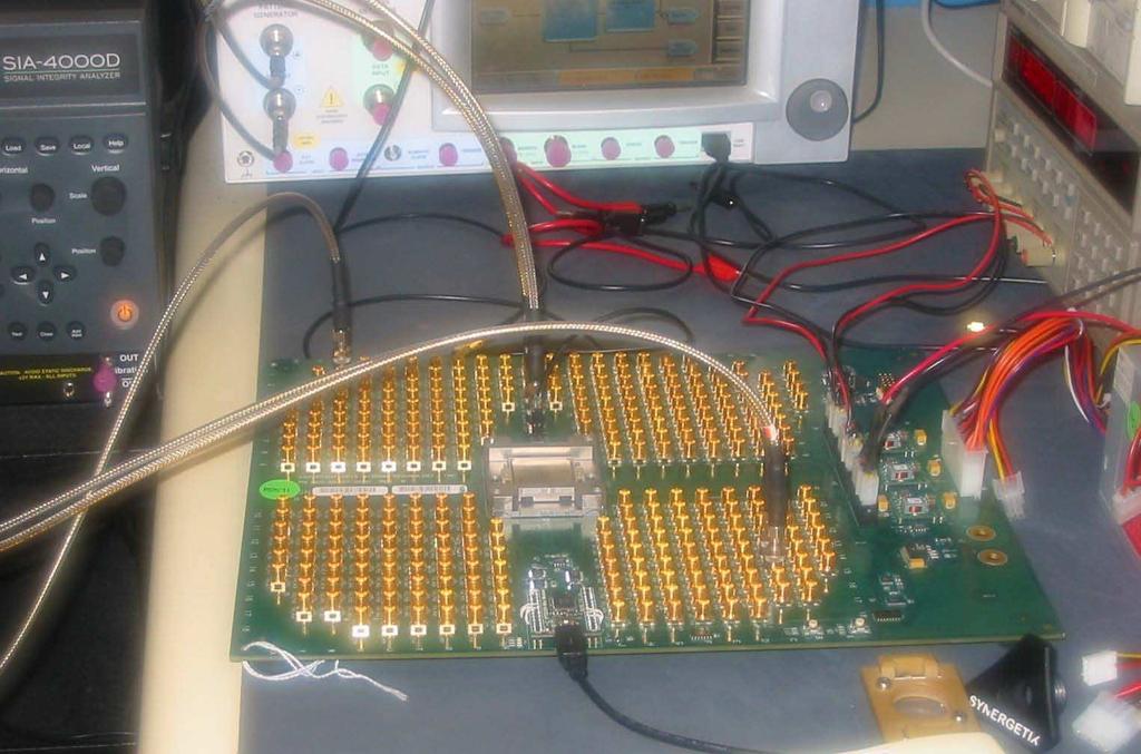


22 HMC Demonstration Platform August 4, Micron Technology, Inc. 22
23 Summary Revolutionary DRAM performance improvement demonstrated by Changing to abstracted high-speed buses Employing 3D packaging using a hybrid of DRAM and logic technologies Pulling in and improving the DRAM controller Marrying DRAM and logic together using many TSVs Completely rethinking DRAM architecture to exploit 3D Managing component health for robust system solutions Result is > 10x bandwidth, < 1/ 3 energy, lower latency Request rates far beyond 2 billion operations per second Logic layer flexibility allows HMC to be tailor-made for multiple platforms and applications Scalable to ANY performance level. I magine the possibilities. August 4, Micron Technology, Inc. 23


24 Energy x Bandwidth I mprovement Per DRAM Generation HMC DDR DDR II DDR3 DDR4 HMC Processor High Speed Links Logic Layer 2011 Micron Technology, Inc. 24
Five Emerging DRAM Interfaces You Should Know for Your Next Design
 Five Emerging DRAM Interfaces You Should Know for Your Next Design By Gopal Raghavan, Cadence Design Systems Producing DRAM chips in commodity volumes and prices to meet the demands of the mobile market
Sort vs. Hash Join Revisited for Near-Memory Execution. Nooshin Mirzadeh, Onur Kocberber, Babak Falsafi, Boris Grot
 Sort vs. Hash Join Revisited for Near-Memory Execution Nooshin Mirzadeh, Onur Kocberber, Babak Falsafi, Boris Grot 1 Near-Memory Processing (NMP) Emerging technology Stacked memory: A logic die w/ a stack
Extending the Benefits of GDDR Beyond Graphics
 Extending the Benefits of GDDR Beyond Graphics Micron High-Performance Graphics Memory Addresses the High-Bandwidth Demands of Networking Today and Tomorrow Overview Key Benefits of High- Performance Graphics
Memory as We Approach a New Horizon
 Memory as We Approach a New Horizon Hot Chips 2016 Memory Tutorial J. Thomas Pawlowski, Chief Technologist, Fellow 2015 2016 Micron Technology, Inc. All rights reserved. Information, products, and/or specifications
High Performance Memory Opportunities in 2.5D Network Flow Processors
 High Performance Memory Opportunities in 2.5D Network Flow Processors Jay Seaton, VP Silicon Operations, Netronome Larry Zu, PhD, President, Sarcina Technology LLC August 6, 2013 2013 Netronome 1 Netronome
White paper FUJITSU Supercomputer PRIMEHPC FX100 Evolution to the Next Generation
 White paper FUJITSU Supercomputer PRIMEHPC FX100 Evolution to the Next Generation Next Generation Technical Computing Unit Fujitsu Limited Contents FUJITSU Supercomputer PRIMEHPC FX100 System Overview
How Good Is Your Memory? An Architect s Look Inside SSDs
 How Good Is Your Memory? An Architect s Look Inside SSDs Michael Abraham (mabraham@micron.com) Business Line Manager Micron Technology, Inc. August 2015 1 Early Storage Optimizations µc NAND Camera SmartMedia
Addressing the Memory Wall
 Lecture 26: Addressing the Memory Wall Parallel Computer Architecture and Programming CMU 15-418/15-618, Spring 2015 Tunes Cage the Elephant Back Against the Wall (Cage the Elephant) This song is for the
Technical Note. Adding ECC to a Data Bus with DDR4 x16 Components. Introduction. TN-40-41: Adding ECC With DDR4 x16 Components.
 Technical Note TN-40-41: Adding ECC With DDR4 Components Introduction Adding ECC to a Data Bus with DDR4 Components Introduction Systems with lower density memory requirements use DRAM components to save
Emerging IC Packaging Platforms for ICT Systems - MEPTEC, IMAPS and SEMI Bay Area Luncheon Presentation
 Emerging IC Packaging Platforms for ICT Systems - MEPTEC, IMAPS and SEMI Bay Area Luncheon Presentation Dr. Li Li Distinguished Engineer June 28, 2016 Outline Evolution of Internet The Promise of Internet
The Memory Hierarchy 1
 The Memory Hierarchy 1 What is a cache? 2 What problem do caches solve? 3 Memory CPU Abstraction: Big array of bytes Memory memory 4 Performance vs 1980 Processor vs Memory Performance Memory is very slow
EFFICIENTLY ENABLING CONVENTIONAL BLOCK SIZES FOR VERY LARGE DIE- STACKED DRAM CACHES
 EFFICIENTLY ENABLING CONVENTIONAL BLOCK SIZES FOR VERY LARGE DIE- STACKED DRAM CACHES MICRO 2011 @ Porte Alegre, Brazil Gabriel H. Loh [1] and Mark D. Hill [2][1] December 2011 [1] AMD Research [2] University
M7: Next Generation SPARC. Hotchips 26 August 12, Stephen Phillips Senior Director, SPARC Architecture Oracle
 M7: Next Generation SPARC Hotchips 26 August 12, 2014 Stephen Phillips Senior Director, SPARC Architecture Oracle Safe Harbor Statement The following is intended to outline our general product direction.
PUSHING THE LIMITS, A PERSPECTIVE ON ROUTER ARCHITECTURE CHALLENGES
 PUSHING THE LIMITS, A PERSPECTIVE ON ROUTER ARCHITECTURE CHALLENGES Greg Hankins APRICOT 2012 2012 Brocade Communications Systems, Inc. 2012/02/28 Lookup Capacity and Forwarding
Stacking Untested Wafers to Improve Yield. The 3D Enigma
 Stacking Untested Wafers to Improve Yield or 3D: Where the Timid Go to Die The 3D Enigma The Promise High Performance Low Power Improved Density More than Moore or at least as much as Moore The Reality
3DIC and the Hybrid Memory Cube
 3DIC and the Hybrid Memory Cube Dean Klein Micron Technology, Inc. 2012 Micron Technology, Inc. All rights reserved. Products are warranted only to meet Micron s production data sheet specifications. Information,
1 Copyright 2013 Oracle and/or its affiliates. All rights reserved.
 1 Copyright 2013 Oracle and/or its affiliates. All rights reserved. Bixby: the Scalability and Coherence Directory ASIC in Oracle's Highly Scalable Enterprise Systems Thomas Wicki and Jürgen Schulz Senior
NAND Flash Architecture and Specification Trends
 NAND Flash Architecture and Specification Trends Michael Abraham (mabraham@micron.com) NAND Solutions Group Architect Micron Technology, Inc. August 2011 1 Topics NAND Flash trends SSD/Enterprise application
IMM128M72D1SOD8AG (Die Revision F) 1GByte (128M x 72 Bit)
 1GByte (128M x 72 Bit)") Product Specification Rev. 1.0 2015 IMM128M72D1SOD8AG (Die Revision F) 1GByte (128M x 72 Bit) 1GB DDR Unbuffered SO-DIMM RoHS Compliant Product Product Specification 1.0 1 IMM128M72D1SOD8AG Version: Rev.
Product Specification Rev. 1.0 2015 IMM128M72D1SOD8AG (Die Revision F) 1GByte (128M x 72 Bit) 1GB DDR Unbuffered SO-DIMM RoHS Compliant Product Product Specification 1.0 1 IMM128M72D1SOD8AG Version: Rev.
An introduction to SDRAM and memory controllers. 5kk73
 An introduction to SDRAM and memory controllers 5kk73 Presentation Outline (part 1) Introduction to SDRAM Basic SDRAM operation Memory efficiency SDRAM controller architecture Conclusions Followed by part
40Gbps+ Full Line Rate, Programmable Network Accelerators for Low Latency Applications SAAHPC 19 th July 2011
 40Gbps+ Full Line Rate, Programmable Network Accelerators for Low Latency Applications SAAHPC 19 th July 2011 Allan Cantle President & Founder www.nallatech.com Company Overview ISI + Nallatech + Innovative
Facilitating IP Development for the OpenCAPI Memory Interface Kevin McIlvain, Memory Development Engineer IBM. Join the Conversation #OpenPOWERSummit
 Facilitating IP Development for the OpenCAPI Memory Interface Kevin McIlvain, Memory Development Engineer IBM Join the Conversation #OpenPOWERSummit Moral of the Story OpenPOWER is the best platform to
Green Memory Solution. Jung-Bae Lee
 Green Memory Solution Jung-Bae Lee Contents Introduction Data Explosion and Data Center Expansion Data Center Issues: Power & Performance Samsung Green Memory Solution History of Green Memory Memory &
IMM64M64D1SOD16AG (Die Revision D) 512MByte (64M x 64 Bit)
 512MByte (64M x 64 Bit)") Product Specification Rev. 2.0 2015 IMM64M64D1SOD16AG (Die Revision D) 512MByte (64M x 64 Bit) 512MB DDR Unbuffered SO-DIMM RoHS Compliant Product Product Specification 2.0 1 IMM64M64D1SOD16AG Version:
Product Specification Rev. 2.0 2015 IMM64M64D1SOD16AG (Die Revision D) 512MByte (64M x 64 Bit) 512MB DDR Unbuffered SO-DIMM RoHS Compliant Product Product Specification 2.0 1 IMM64M64D1SOD16AG Version:
The 3D-Memory Evolution
 The 3D-Memory Evolution ISC 2015 /, Director Marcom + SBD EMEA Legal Disclaimer This presentation is intended to provide information concerning computer and memory industries. We do our best to make sure
DRAM Main Memory. Dual Inline Memory Module (DIMM)
") DRAM Main Memory Dual Inline Memory Module (DIMM) Memory Technology Main memory serves as input and output to I/O interfaces and the processor. DRAMs for main memory, SRAM for caches Metrics: Latency,
DRAM Main Memory Dual Inline Memory Module (DIMM) Memory Technology Main memory serves as input and output to I/O interfaces and the processor. DRAMs for main memory, SRAM for caches Metrics: Latency,
Samsung Memory DDR4 SDRAM
 Samsung Memory SDRAM The new generation of high-performance, power-efficient memory that delivers great reliability for enterprise applications 205 Samsung Electronics Co. Brochure An optimized memory
Industry Trends in 3D and Advanced Packaging
 Industry Trends in 3D and Advanced Packaging Outline Industry System and Component Challenges & Trends 3D and Advanced Packaging Value-proposition and Client Examples 3D Technology Details 3DIC / 3DTSV
Agenda. System Performance Scaling of IBM POWER6 TM Based Servers
 System Performance Scaling of IBM POWER6 TM Based Servers Jeff Stuecheli Hot Chips 19 August 2007 Agenda Historical background POWER6 TM chip components Interconnect topology Cache Coherence strategies
Future of Interconnect Fabric A Contrarian View. Shekhar Borkar June 13, 2010 Intel Corp. 1
 Future of Interconnect Fabric A ontrarian View Shekhar Borkar June 13, 2010 Intel orp. 1 Outline Evolution of interconnect fabric On die network challenges Some simple contrarian proposals Evaluation and
IMM128M64D1DVD8AG (Die Revision F) 1GByte (128M x 64 Bit)
 1GByte (128M x 64 Bit)") Product Specification Rev. 1.0 2015 IMM128M64D1DVD8AG (Die Revision F) 1GByte (128M x 64 Bit) 1GB DDR VLP Unbuffered DIMM RoHS Compliant Product Product Specification 1.0 1 IMM128M64D1DVD8AG Version: Rev.
Product Specification Rev. 1.0 2015 IMM128M64D1DVD8AG (Die Revision F) 1GByte (128M x 64 Bit) 1GB DDR VLP Unbuffered DIMM RoHS Compliant Product Product Specification 1.0 1 IMM128M64D1DVD8AG Version: Rev.
THE PATH TO EXASCALE COMPUTING. Bill Dally Chief Scientist and Senior Vice President of Research
 THE PATH TO EXASCALE COMPUTING Bill Dally Chief Scientist and Senior Vice President of Research The Goal: Sustained ExaFLOPs on problems of interest 2 Exascale Challenges Energy efficiency Programmability
DDR SDRAM UDIMM. Draft 9/ 9/ MT18VDDT6472A 512MB 1 MT18VDDT12872A 1GB For component data sheets, refer to Micron s Web site:
 DDR SDRAM UDIMM MT18VDDT6472A 512MB 1 MT18VDDT12872A 1GB For component data sheets, refer to Micron s Web site: www.micron.com 512MB, 1GB (x72, ECC, DR) 184-Pin DDR SDRAM UDIMM Features Features 184-pin,
DDR2 SDRAM UDIMM MT16HTF25664AZ 2GB MT16HTF51264AZ 4GB For component data sheets, refer to Micron s Web site:
 DDR2 SDRAM UDIMM MT16HTF25664AZ 2GB MT16HTF51264AZ 4GB For component data sheets, refer to Micron s Web site: www.micron.com 2GB, 4GB (x64, DR): 240-Pin DDR2 SDRAM UDIMM Features Features 240-pin, unbuffered
Memories: Memory Technology
 Memories: Memory Technology Z. Jerry Shi Assistant Professor of Computer Science and Engineering University of Connecticut * Slides adapted from Blumrich&Gschwind/ELE475 03, Peh/ELE475 * Memory Hierarchy
CS311 Lecture 21: SRAM/DRAM/FLASH
 S 14 L21-1 2014 CS311 Lecture 21: SRAM/DRAM/FLASH DARM part based on ISCA 2002 tutorial DRAM: Architectures, Interfaces, and Systems by Bruce Jacob and David Wang Jangwoo Kim (POSTECH) Thomas Wenisch (University
NVIDIA nforce IGP TwinBank Memory Architecture
 NVIDIA nforce IGP TwinBank Memory Architecture I. Memory Bandwidth and Capacity There s Never Enough With the recent advances in PC technologies, including high-speed processors, large broadband pipelines,
Industry Collaboration and Innovation
 Industry Collaboration and Innovation OpenCAPI Topics Industry Background Technology Overview Design Enablement OpenCAPI Consortium Industry Landscape Key changes occurring in our industry Historical microprocessor
Netronome NFP: Theory of Operation
 WHITE PAPER Netronome NFP: Theory of Operation TO ACHIEVE PERFORMANCE GOALS, A MULTI-CORE PROCESSOR NEEDS AN EFFICIENT DATA MOVEMENT ARCHITECTURE. CONTENTS 1. INTRODUCTION...1 2. ARCHITECTURE OVERVIEW...2
DDR SDRAM UDIMM MT16VDDT6464A 512MB MT16VDDT12864A 1GB MT16VDDT25664A 2GB
 DDR SDRAM UDIMM MT16VDDT6464A 512MB MT16VDDT12864A 1GB MT16VDDT25664A 2GB For component data sheets, refer to Micron s Web site: www.micron.com 512MB, 1GB, 2GB (x64, DR) 184-Pin DDR SDRAM UDIMM Features
IMM64M72D1SCS8AG (Die Revision D) 512MByte (64M x 72 Bit)
 512MByte (64M x 72 Bit)") Product Specification Rev. 1.0 2015 IMM64M72D1SCS8AG (Die Revision D) 512MByte (64M x 72 Bit) RoHS Compliant Product Product Specification 1.0 1 IMM64M72D1SCS8AG Version: Rev. 1.0, MAY 2015 1.0 - Initial
Product Specification Rev. 1.0 2015 IMM64M72D1SCS8AG (Die Revision D) 512MByte (64M x 72 Bit) RoHS Compliant Product Product Specification 1.0 1 IMM64M72D1SCS8AG Version: Rev. 1.0, MAY 2015 1.0 - Initial
IBM XIV Storage System
 IBM XIV Storage System Technical Description IBM XIV Storage System Storage Reinvented Performance The IBM XIV Storage System offers a new level of high-end disk system performance and reliability. It
Maximizing heterogeneous system performance with ARM interconnect and CCIX
 Maximizing heterogeneous system performance with ARM interconnect and CCIX Neil Parris, Director of product marketing Systems and software group, ARM Teratec June 2017 Intelligent flexible cloud to enable
A Single Chip Shared Memory Switch with Twelve 10Gb Ethernet Ports
 A Single Chip Shared Memory Switch with Twelve 10Gb Ethernet Ports Takeshi Shimizu, Yukihiro Nakagawa, Sridhar Pathi, Yasushi Umezawa, Takashi Miyoshi, Yoichi Koyanagi, Takeshi Horie, Akira Hattori Hot
Boosting the Performance of FPGA-based Graph Processor using Hybrid Memory Cube: A Case for Breadth First Search
 Boosting the Performance of FPGA-based Graph Processor using Hybrid Memory Cube: A Case for Breadth First Search Jialiang Zhang, Soroosh Khoram and Jing Li 1 Outline Background Big graph analytics Hybrid
4GB Unbuffered VLP DDR3 SDRAM DIMM with SPD
 4GB Unbuffered VLP DDR3 SDRAM DIMM with SPD Ordering Information Part Number Bandwidth Speed Grade Max Frequency CAS Latency Density Organization Component Composition 78.B1GE3.AFF0C 12.8GB/sec 1600Mbps
DDR SDRAM UDIMM MT8VDDT3264A 256MB MT8VDDT6464A 512MB For component data sheets, refer to Micron s Web site:
 DDR SDRAM UDIMM MT8VDDT3264A 256MB MT8VDDT6464A 512MB For component data sheets, refer to Micron s Web site: www.micron.com 256MB, 512MB (x64, SR) 184-Pin DDR SDRAM UDIMM Features Features 184-pin, unbuffered
Key Points. Rotational delay vs seek delay Disks are slow. Techniques for making disks faster. Flash and SSDs
 IO 1 Today IO 2 Key Points CPU interface and interaction with IO IO devices The basic structure of the IO system (north bridge, south bridge, etc.) The key advantages of high speed serial lines. The benefits
Open Innovation with Power8
 2011 IBM Power Systems Technical University October 10-14 Fontainebleau Miami Beach Miami, FL IBM Open Innovation with Power8 Jeffrey Stuecheli Power Processor Development Copyright IBM Corporation 2013
Organization Row Address Column Address Bank Address Auto Precharge 128Mx8 (1GB) based module A0-A13 A0-A9 BA0-BA2 A10
 based module A0-A13 A0-A9 BA0-BA2 A10") GENERAL DESCRIPTION The Gigaram is ECC Registered Dual-Die DIMM with 1.25inch (30.00mm) height based on DDR2 technology. DIMMs are available as ECC modules in 256Mx72 (2GByte) organization and density,
GENERAL DESCRIPTION The Gigaram is ECC Registered Dual-Die DIMM with 1.25inch (30.00mm) height based on DDR2 technology. DIMMs are available as ECC modules in 256Mx72 (2GByte) organization and density,
TETRIS: Scalable and Efficient Neural Network Acceleration with 3D Memory
 TETRIS: Scalable and Efficient Neural Network Acceleration with 3D Memory Mingyu Gao, Jing Pu, Xuan Yang, Mark Horowitz, Christos Kozyrakis Stanford University Platform Lab Review Feb 2017 Deep Neural
Options. Data Rate (MT/s) CL = 3 CL = 2.5 CL = 2-40B PC PC PC
 CL = 3 CL = 2.5 CL = 2-40B PC PC PC") DDR SDRAM UDIMM MT16VDDF6464A 512MB 1 MT16VDDF12864A 1GB 1 For component data sheets, refer to Micron s Web site: www.micron.com 512MB, 1GB (x64, DR) 184-Pin DDR SDRAM UDIMM Features Features 184-pin,
DDR SDRAM UDIMM MT16VDDF6464A 512MB 1 MT16VDDF12864A 1GB 1 For component data sheets, refer to Micron s Web site: www.micron.com 512MB, 1GB (x64, DR) 184-Pin DDR SDRAM UDIMM Features Features 184-pin,
2GB DDR3 SDRAM SODIMM with SPD
 2GB DDR3 SDRAM SODIMM with SPD Ordering Information Part Number Bandwidth Speed Grade Max Frequency CAS Latency Density Organization Component Composition Number of Rank 78.A2GC6.AF1 10.6GB/sec 1333Mbps
Samsung emcp. WLI DDP Package. Samsung Multi-Chip Packages can help reduce the time to market for handheld devices BROCHURE
 Samsung emcp Samsung Multi-Chip Packages can help reduce the time to market for handheld devices WLI DDP Package Deliver innovative portable devices more quickly. Offer higher performance for a rapidly
Main Memory Systems. Department of Electrical Engineering Stanford University Lecture 5-1
 Lecture 5 Main Memory Systems Department of Electrical Engineering Stanford University http://eeclass.stanford.edu/ee282 Lecture 5-1 Announcements If you don t have a group of 3, contact us ASAP HW-1 is
Memory Systems IRAM. Principle of IRAM
 Memory Systems 165 other devices of the module will be in the Standby state (which is the primary state of all RDRAM devices) or another state with low-power consumption. The RDRAM devices provide several
Overcoming the Memory System Challenge in Dataflow Processing. Darren Jones, Wave Computing Drew Wingard, Sonics
 Overcoming the Memory System Challenge in Dataflow Processing Darren Jones, Wave Computing Drew Wingard, Sonics Current Technology Limits Deep Learning Performance Deep Learning Dataflow Graph Existing
Networks for Multi-core Chips A A Contrarian View. Shekhar Borkar Aug 27, 2007 Intel Corp.
 Networks for Multi-core hips A A ontrarian View Shekhar Borkar Aug 27, 2007 Intel orp. 1 Outline Multi-core system outlook On die network challenges A simple contrarian proposal Benefits Summary 2 A Sample
Future Memories. Jim Handy OBJECTIVE ANALYSIS
 Future Memories Jim Handy OBJECTIVE ANALYSIS Hitting a Brick Wall OBJECTIVE ANALYSIS www.objective-analysis.com Panelists Michael Miller VP Technology, Innovation & Systems Applications MoSys Christophe
Toward a Memory-centric Architecture
 Toward a Memory-centric Architecture Martin Fink EVP & Chief Technology Officer Western Digital Corporation August 8, 2017 1 SAFE HARBOR DISCLAIMERS Forward-Looking Statements This presentation contains
Messaging Overview. Introduction. Gen-Z Messaging
 Page 1 of 6 Messaging Overview Introduction Gen-Z is a new data access technology that not only enhances memory and data storage solutions, but also provides a framework for both optimized and traditional
DDR SDRAM SODIMM MT8VDDT1664H 128MB 1. MT8VDDT3264H 256MB 2 MT8VDDT6464H 512MB For component data sheets, refer to Micron s Web site:
 SODIMM MT8VDDT1664H 128MB 1 128MB, 256MB, 512MB (x64, SR) 200-Pin SODIMM Features MT8VDDT3264H 256MB 2 MT8VDDT6464H 512MB For component data sheets, refer to Micron s Web site: www.micron.com Features
POWER7: IBM's Next Generation Server Processor
 Hot Chips 21 POWER7: IBM's Next Generation Server Processor Ronald Kalla Balaram Sinharoy POWER7 Chief Engineer POWER7 Chief Core Architect Acknowledgment: This material is based upon work supported by
Lecture 15: DRAM Main Memory Systems. Today: DRAM basics and innovations (Section 2.3)
") Lecture 15: DRAM Main Memory Systems Today: DRAM basics and innovations (Section 2.3) 1 Memory Architecture Processor Memory Controller Address/Cmd Bank Row Buffer DIMM Data DIMM: a PCB with DRAM chips
Lecture 15: DRAM Main Memory Systems Today: DRAM basics and innovations (Section 2.3) 1 Memory Architecture Processor Memory Controller Address/Cmd Bank Row Buffer DIMM Data DIMM: a PCB with DRAM chips
Innovations in Non-Volatile Memory 3D NAND and its Implications May 2016 Rob Peglar, VP Advanced Storage,
 Innovations in Non-Volatile Memory 3D NAND and its Implications May 2016 Rob Peglar, VP Advanced Storage, Micron @peglarr 2015 Micron Technology, Inc All rights reserved Products are warranted only to
BREAKING THE MEMORY WALL
 BREAKING THE MEMORY WALL CS433 Fall 2015 Dimitrios Skarlatos OUTLINE Introduction Current Trends in Computer Architecture 3D Die Stacking The memory Wall Conclusion INTRODUCTION Ideal Scaling of power
Technology challenges and trends over the next decade (A look through a 2030 crystal ball) Al Gara Intel Fellow & Chief HPC System Architect
 Al Gara Intel Fellow & Chief HPC System Architect") Technology challenges and trends over the next decade (A look through a 2030 crystal ball) Al Gara Intel Fellow & Chief HPC System Architect Today s Focus Areas For Discussion Will look at various technologies
Technology challenges and trends over the next decade (A look through a 2030 crystal ball) Al Gara Intel Fellow & Chief HPC System Architect Today s Focus Areas For Discussion Will look at various technologies
A 400Gbps Multi-Core Network Processor
 A 400Gbps Multi-Core Network Processor James Markevitch, Srinivasa Malladi Cisco Systems August 22, 2017 Legal THE INFORMATION HEREIN IS PROVIDED ON AN AS IS BASIS, WITHOUT ANY WARRANTIES OR REPRESENTATIONS,
HEAT (Hardware enabled Algorithmic tester) for 2.5D HBM Solution
 for 2.5D HBM Solution") HEAT (Hardware enabled Algorithmic tester) for 2.5D HBM Solution Kunal Varshney, Open-Silicon Ganesh Venkatkrishnan, Open-Silicon Pankaj Prajapati, Open-Silicon May 9, 9, 2016 1 Agenda High Bandwidth Memory
HEAT (Hardware enabled Algorithmic tester) for 2.5D HBM Solution Kunal Varshney, Open-Silicon Ganesh Venkatkrishnan, Open-Silicon Pankaj Prajapati, Open-Silicon May 9, 9, 2016 1 Agenda High Bandwidth Memory
Rethinking On-chip DRAM Cache for Simultaneous Performance and Energy Optimization
 Rethinking On-chip DRAM Cache for Simultaneous Performance and Energy Optimization Fazal Hameed and Jeronimo Castrillon Center for Advancing Electronics Dresden (cfaed), Technische Universität Dresden,
POWER7: IBM's Next Generation Server Processor
 POWER7: IBM's Next Generation Server Processor Acknowledgment: This material is based upon work supported by the Defense Advanced Research Projects Agency under its Agreement No. HR0011-07-9-0002 Outline
Features. DDR2 UDIMM with ECC Product Specification. Rev. 1.2 Aug. 2011
 Features 240pin, unbuffered dual in-line memory module (UDIMM) Error Check Correction (ECC) Support Fast data transfer rates: PC2-4200, PC3-5300, PC3-6400 Single or Dual rank 512MB (64Meg x 72), 1GB(128
Interposer Technology: Past, Now, and Future
 Interposer Technology: Past, Now, and Future Shang Y. Hou TSMC 侯上勇 3D TSV: Have We Waited Long Enough? Garrou (2014): A Little More Patience Required for 2.5/3D All things come to those who wait In 2016,
DDR2 SDRAM UDIMM MT8HTF12864AZ 1GB
 Features DDR2 SDRAM UDIMM MT8HTF12864AZ 1GB For component data sheets, refer to Micron's Web site: www.micron.com Figure 1: 240-Pin UDIMM (MO-237 R/C D) Features 240-pin, unbuffered dual in-line memory
DFT Trends in the More than Moore Era. Stephen Pateras Mentor Graphics
 DFT Trends in the More than Moore Era Stephen Pateras Mentor Graphics steve_pateras@mentor.com Silicon Valley Test Conference 2011 1 Outline Semiconductor Technology Trends DFT in relation to: Increasing
Thermal-Aware Memory Management Unit of 3D- Stacked DRAM for 3D High Definition (HD) Video
 Video") Thermal-Aware Memory Management Unit of 3D- Stacked DRAM for 3D High Definition (HD) Video Chih-Yuan Chang, Po-Tsang Huang, Yi-Chun Chen, Tian-Sheuan Chang and Wei Hwang Department of Electronics Engineering
Thermal-Aware Memory Management Unit of 3D- Stacked DRAM for 3D High Definition (HD) Video Chih-Yuan Chang, Po-Tsang Huang, Yi-Chun Chen, Tian-Sheuan Chang and Wei Hwang Department of Electronics Engineering
IMM64M64D1DVS8AG (Die Revision D) 512MByte (64M x 64 Bit)
 512MByte (64M x 64 Bit)") Product Specification Rev. 1.0 2015 IMM64M64D1DVS8AG (Die Revision D) 512MByte (64M x 64 Bit) 512MB DDR VLP Unbuffered DIMM RoHS Compliant Product Product Specification 1.0 1 IMM64M64D1DVS8AG Version:
Product Specification Rev. 1.0 2015 IMM64M64D1DVS8AG (Die Revision D) 512MByte (64M x 64 Bit) 512MB DDR VLP Unbuffered DIMM RoHS Compliant Product Product Specification 1.0 1 IMM64M64D1DVS8AG Version:
World s most advanced data center accelerator for PCIe-based servers
 NVIDIA TESLA P100 GPU ACCELERATOR World s most advanced data center accelerator for PCIe-based servers HPC data centers need to support the ever-growing demands of scientists and researchers while staying
Enabling Technology for the Cloud and AI One Size Fits All?
 Enabling Technology for the Cloud and AI One Size Fits All? Tim Horel Collaborate. Differentiate. Win. DIRECTOR, FIELD APPLICATIONS The Growing Cloud Global IP Traffic Growth 40B+ devices with intelligence
3D TECHNOLOGIES: SOME PERSPECTIVES FOR MEMORY INTERCONNECT AND CONTROLLER
 3D TECHNOLOGIES: SOME PERSPECTIVES FOR MEMORY INTERCONNECT AND CONTROLLER CODES+ISSS: Special session on memory controllers Taipei, October 10 th 2011 Denis Dutoit, Fabien Clermidy, Pascal Vivet {denis.dutoit@cea.fr}
Tile Processor (TILEPro64)
") Tile Processor Case Study of Contemporary Multicore Fall 2010 Agarwal 6.173 1 Tile Processor (TILEPro64) Performance # of cores On-chip cache (MB) Cache coherency Operations (16/32-bit BOPS) On chip bandwidth
Tile Processor Case Study of Contemporary Multicore Fall 2010 Agarwal 6.173 1 Tile Processor (TILEPro64) Performance # of cores On-chip cache (MB) Cache coherency Operations (16/32-bit BOPS) On chip bandwidth
Chapter 2: Memory Hierarchy Design (Part 3) Introduction Caches Main Memory (Section 2.2) Virtual Memory (Section 2.4, Appendix B.4, B.
 Introduction Caches Main Memory (Section 2.2) Virtual Memory (Section 2.4, Appendix B.4, B.") Chapter 2: Memory Hierarchy Design (Part 3) Introduction Caches Main Memory (Section 2.2) Virtual Memory (Section 2.4, Appendix B.4, B.5) Memory Technologies Dynamic Random Access Memory (DRAM) Optimized
Chapter 2: Memory Hierarchy Design (Part 3) Introduction Caches Main Memory (Section 2.2) Virtual Memory (Section 2.4, Appendix B.4, B.5) Memory Technologies Dynamic Random Access Memory (DRAM) Optimized
1. The values of t RCD and t RP for -335 modules show 18ns to align with industry specifications; actual DDR SDRAM device specifications are 15ns.
 UDIMM MT4VDDT1664A 128MB MT4VDDT3264A 256MB For component data sheets, refer to Micron s Web site: www.micron.com 128MB, 256MB (x64, SR) 184-Pin UDIMM Features Features 184-pin, unbuffered dual in-line
Intel: Driving the Future of IT Technologies. Kevin C. Kahn Senior Fellow, Intel Labs Intel Corporation
 Research @ Intel: Driving the Future of IT Technologies Kevin C. Kahn Senior Fellow, Intel Labs Intel Corporation kp Intel Labs Mission To fuel Intel s growth, we deliver breakthrough technologies that
Forging a Future in Memory: New Technologies, New Markets, New Applications
 Forging a Future in Memory: New Technologies, New Markets, New Applications Ed Doller V.P. Chief Memory Systems Architect Non-Volatile Memory Seminar Hot Chips Conference August 22, 2010 Memorial Auditorium
Optimize your system designs using Flash memory
 Optimize your system designs using Flash memory Howard Cheng Sr. Segment Applications Manager Embedded Solutions Group, Micron 2012 Micron Technology, Inc. All rights reserved. Products are warranted only
Kevin Donnelly, General Manager, Memory and Interface Division
 Kevin Donnelly, General Manager, Memory and Interface Division Robust system solutions including memory and serial link interfaces that increase SoC and system quality. Driving Factors for Systems Today
DDR SDRAM SODIMM MT16VDDF6464H 512MB MT16VDDF12864H 1GB
 SODIMM MT16VDDF6464H 512MB MT16VDDF12864H 1GB 512MB, 1GB (x64, DR) 200-Pin DDR SODIMM Features For component data sheets, refer to Micron s Web site: www.micron.com Features 200-pin, small-outline dual
The Evolution of Mobile
 The Evolution of Mobile and its impact on storage architecture Jonathan Hubert Director, Strategic Marketing Micron Technology Mobile Memory Workshop 2011 Wireless Data Rates Doubling Every 18 Months 2
Interconnect Challenges in a Many Core Compute Environment. Jerry Bautista, PhD Gen Mgr, New Business Initiatives Intel, Tech and Manuf Grp
 Interconnect Challenges in a Many Core Compute Environment Jerry Bautista, PhD Gen Mgr, New Business Initiatives Intel, Tech and Manuf Grp Agenda Microprocessor general trends Implications Tradeoffs Summary
Technical Note Using Micron Asynchronous PSRAM with the NXP LPC2292 and LPC2294 Microcontrollers
 TN-45-29: Using Micron Async PSRAM with NXP LPC2292/2294 Introduction Technical Note Using Micron Asynchronous PSRAM with the NXP LPC2292 and LPC2294 Microcontrollers Introduction The NXP LPC2292 and LPC2294
p5 520 server Robust entry system designed for the on demand world Highlights
 Robust entry system designed for the on demand world IBM p5 520 server _` p5 520 rack system with I/O drawer Highlights Innovative, powerful, affordable, open and adaptable UNIX and Linux environment system
Extreme Scale Computer Architecture: Energy Efficiency from the Ground Up
 Extreme Scale Computer Architecture: Energy Efficiency from the Ground Up Josep Torrellas Department of Computer Science University of Illinois at Urbana-Champaign http://iacoma.cs.uiuc.edu Design, Automation
Linux Storage System Bottleneck Exploration
 Linux Storage System Bottleneck Exploration Bean Huo / Zoltan Szubbocsev Beanhuo@micron.com / zszubbocsev@micron.com 215 Micron Technology, Inc. All rights reserved. Information, products, and/or specifications
Comparing UFS and NVMe Storage Stack and System-Level Performance in Embedded Systems
 Comparing UFS and NVMe Storage Stack and System-Level Performance in Embedded Systems Bean Huo, Blair Pan, Peter Pan, Zoltan Szubbocsev Micron Technology Introduction Embedded storage systems have experienced
NetSpeed ORION: A New Approach to Design On-chip Interconnects. August 26 th, 2013
 NetSpeed ORION: A New Approach to Design On-chip Interconnects August 26 th, 2013 INTERCONNECTS BECOMING INCREASINGLY IMPORTANT Growing number of IP cores Average SoCs today have 100+ IPs Mixing and matching
Memory Challenges. Issues & challenges in memory design: Cost Performance Power Scalability
 Memory Devices 1 Memory Challenges Issues & challenges in memory design: Cost Performance Power Scalability 2 Memory - Overview Definitions: RAM random access memory DRAM dynamic RAM SRAM static RAM Volatile
Introduction to Multiprocessors (Part I) Prof. Cristina Silvano Politecnico di Milano
 Prof. Cristina Silvano Politecnico di Milano") Introduction to Multiprocessors (Part I) Prof. Cristina Silvano Politecnico di Milano Outline Key issues to design multiprocessors Interconnection network Centralized shared-memory architectures Distributed
Introduction to Multiprocessors (Part I) Prof. Cristina Silvano Politecnico di Milano Outline Key issues to design multiprocessors Interconnection network Centralized shared-memory architectures Distributed
Power Technology For a Smarter Future
 2011 IBM Power Systems Technical University October 10-14 Fontainebleau Miami Beach Miami, FL IBM Power Technology For a Smarter Future Jeffrey Stuecheli Power Processor Development Copyright IBM Corporation
3D systems-on-chip. A clever partitioning of circuits to improve area, cost, power and performance. The 3D technology landscape
 Edition April 2017 Semiconductor technology & processing 3D systems-on-chip A clever partitioning of circuits to improve area, cost, power and performance. In recent years, the technology of 3D integration