Mike Mitchell DSP Specialist, Austin, TX
|
|
|
- Jody Patterson
- 6 years ago
- Views:
Transcription


1 Zynq for Video Applications Mike Mitchell DSP Specialist, Austin, TX
2 Serial vs. Parallel DSP Processing Standard DSP Processor ALU Sequential (Generic DSP) Data In Data In FPGA - Fully Parallel Implementation (Virtex-6 FPGA) Reg Reg Reg Reg Coefficients 2016 clock cycles needed X + Reg Single-MAC Unit C0 X C1 X C operations in 1 clock cycle C2 X + C3 Data Out X C2015 X Data Out 1.2 GHz 2016 clock cycles = 595 KSPS 600 MHz 1 clock cycle = 600 MSPS demuxed filter architectures can enable even higher data rates
3 Software vs Hardware Acceleration Different FFT architectures can push performance even higher, consider sub 5us 2D FFT (GSPS) 550MSPS rate After pipeline is filled 5.4MSPS rate

4 Xilinx DSP Performance Leadership DSP Performance Gap Performanc ce (Algorithmic and Proces ssor Forecast) 2300 GMACs 1000 GMACs 32 GMACs 10 GMACs Virtex -7 Virtex -6 Spartan -6 Traditional DSP Architectures DSP Processors: TI DM GHz: 8.8GMACs (16 bit mults/cycle) TI DM MHz: 6GMACs (16 bit mults/cycle) Time Source: Forward Concepts
5 Comparing TI DM648 Functionality and Zynq

 8.")
6 TI TMS320DM MB address space DDR2 (32 bit) EMIFA 16 bit interface MHz MHz Table 6.42 pg 112 tms320dm648.pdf Up to 1,1GHz C64x clock rates 8 MIPs/MHz 6 ALUs, 2 Multipliers (32, 16 or 8 bit ops) 8.8GMACs 90nm process technology 32KB I/D L1 Cache 512KB L2 64KB ROM
7 TI DM648 vs Zynq TI TMS320DM648 90nm process Up to 1.1GHz C64x 8.0 DMIPS/MHz max (based on clock frequency) 32KB I/D cache 512KB L2 cache 64KB ROM 8.8GMACs max (based on 1.1GHz clock frequency) Zynq 28nm process Dual, MHz Cortex A9 + NEON coprocessor 2.5 DMIPs/MHz & 2.88 CoreMark/MHz 32KB I/D cache 512KB L2 cache 256KB on chip memory NEON has FP (2MFLOPS/MHz) + fixed point SIMD capability per core 7020 device has 220 DSP48s (628MHz -3 speed grade) for 138.1GMACs of performance Speed grades -1 (464MHz), -2 (550), -3 (628)
8 Comparing TI DM8148 Functionality and Zynq
9 TI TMS320DM8148 Up to 750MHz C674x 32KB L1, 256KB L2 6 ALUs, 2 Multipliers (32, 16 or 8 bit ops) 8.8GMACs, 6 MFLOPs/MHz 45nm process technology Cortex A8 32KB I/D L1 Cache 512KB L2 Cache 64KB RAM
10 TI DM8148 vs Zynq TI TMS320DM648 45nm process Up to 1GHz Cortex A8 + NEON coprocessor 2.0 DMIPs/MHz 32KB I/D cache 512KB L2 cache 64KB on chip memory Up to 750MHz C674x 8.0 MMACs/MHz max (based on clock frequency) 6MFLOPs/MHz (based on clock frequency) Zynq 28nm process Dual, MHz Cortex A9 + NEON coprocessor 2.5 DMIPs/MHz 32KB I/D cache 512KB L2 cache 256KB on chip memory NEON has FP (2MFLOPS/MHz) + fixed point SIMD capability per core 7020 device has 220 DSP48s (628MHz -3 speed grade) for 138.1GMACs of performance Speed grades -1 (464MHz), -2 (550), -3 (628)
11 Zynq A Full Custom, Single Chip ASSP 16/32 bit, 533MHz Processing System I/O MUX 2x SPI 2x I2C 2x CAN 2x UART GPIO 2x SDIO with DMA 2x USB with DMA 2x GigE with DMA Static Memory Controller Quad-SPI, NAND, NOR AMBA Switches MI O Dynamic Memory Controller DDR3, DDR2, LPDDR2 ARM CoreSight Multi-core & Trace Debug NEON / FPU Engine AMBA Switches NEON / FPU Engine Cortex -A9 MPCore Cortex -A9 MPCore 32/32 KB I/D Caches 32/32 KB I/D Caches 512 KB L2 Cache Timer Counters Snoop Control Unit (SCU) 256 KB On-Chip Memory General Interrupt Controller DMA Configuration AMBA AMBA Switches ACP Programmable Logic: System Gates, DSP, RAM AXI HP Ports Path to OCM/DDR ACP 64 bit cache coherent access to CPU Data in L1/L2 cache Multi-Standards I/Os (3.3V & High Speed 1.8V) XADC 2x32 bit AXI master 2x32 bit AXI slaves PCIe Multi-Standards I/Os (3.3V & High Speed 1.8V) Multi Gigabit Transceivers
12 Zynq Targeted to Signal Processing Applications Processor Core Complex Dual ARM Cortex -A9 MPCore with NEON extensions Single / Double Precision Floating Point support 2 MFLOPS/MHz Up to 800 MHz operation Over 3000 Internal Interconnects Up to 100Gb of BW Memory-mapped interfaces Enables Massive Parallel Processing Up to 900 DSP blocks delivering over 1080 GMACs (symmetric FIR implementation) Application specific custom hardware accelerator AMBA Open Standard Interconnnect High bandwidth interconnect between processing system and programmable logic ACP port for enhanced hardware acceleration and cache coherency for additional soft processors Processing System Ready to Program
13 Zynq High Performance (HP) Ports
14 SW vs HW Task Implementation Decisions Keep it in Software Not in critical path Enough free cycles Easier to code in software than hardware Use math library functions NEON coprocessor Supports integer vector operations Single floating point operations Move to Hardware Higher performance Architecture determines area / throughput (ie: reference FFT page 3 & size vs latency discussion) Customize to meet your needs & reduce processor bandwidth requirements Excellent for iterative, pipelined & parallel processing Move to another processor Both Microblaze & Picoblaze can exist in the fabric
.")

15 TI OMAP35xx vs Zynq for H.264 CODEC - h.264 Base CODEC is C code (ie: not optimized for NEON coprocessor or C64x VLIW). C code was also optimized for C64x VLIW core & CA8 NEON coprocessor. Use of Cortex A8 + NEON shows better performance than the C64x VLIW core in an OMAP3530. Demonstrates required processor clock rate compared to achieve the same VGA 30fps 1Mbps video streams for a Cortex A8 vs. OMAP3430 lower clock rate MHz means better performance Demonstrates NEON coprocessor is better than OMAP3530 C64x VLIW core.

16 Zynq NEON 3 rd party ecosystem Image, Audio, Video H.264, VC1, MPEG-4 VP6/7, MPEG-4, VC-1, H.264 (enc+dec), video stabilization MPEG-4, MPEG-2, H.263, H.264, WMV9, VC1, DD+ MPEG-4, H.263, H.264, WMV9, audio H.264, VC1 TEAMSpirit voice & video drawelements Finland Espico Ltd MPEG-4 GUI visual efffects 2D GUI library Audio: low-bitrate & digital theater, consulting CoreAVC ultra fast codec H.264, MPEG-4, H.263, WMV MobiClip ARM NEON widely supported by software partners Adobe Codecs Multichannel audio processing Flash products Full list on NEON ecosystem page


17 Xilinx IP Library for Camera Systems Same IP supports video processing applications and displays Memory Buffer Image Sensor Image Processing Video Processing Compression Connectivity Video Out, Ethernet, etc. Cortex A9 Command and control Auto White Balance Auto Exposure Auto Focus Image Processing Defective Pixel Correction Color Filter Array Interp Color Correction Matrix Gamma Correction Color Space conversion Statistics Module Noise Reduction Edge Enhancement Video Processing Video Scaler On-Screen-Display Motion Adaptive Noise Reduction Image Characterization Object Segmentation Memory and timing Timing Controller MPMC + VFBC Video DMA Compression H.264/MPEG-4 MPEG-2 MPEG-4 JPEG JPEG-2000 Connectivity 10/100/1G Ethernet SDI Ethernet AVB Display port Vx1, Vx4 HDMI/DVI Firewire GigE Vision Camera Link


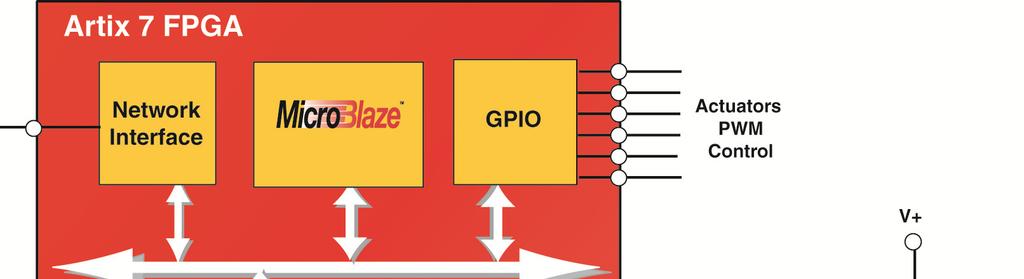
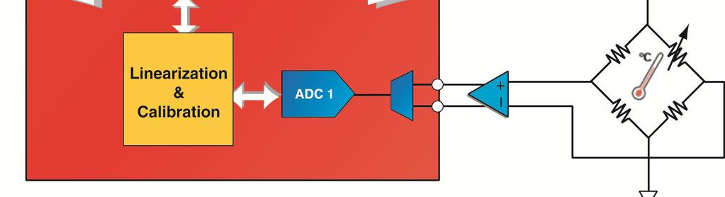
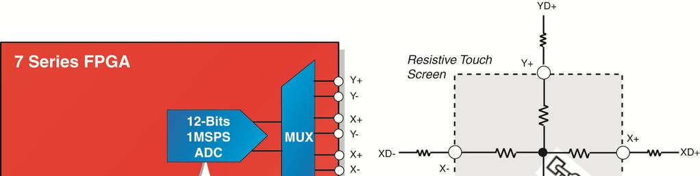
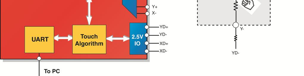
18 Some XADC Examples Motor Control / Energy Conversion Sensor Interfacing Off load CPU Sensor Compensation Touch Interface
19 Video Applications
20 Computer Vision Processing Complexity High to medium data rates Medium algorithm complexity Image Pre-processing Lens Correction Segmentation And Object Analysis Heuristics or Expert System Ultra high data rates Low algorithm complexity (complexity implies code amount for a HLL) Low data rates High algorithm complexity CPU type tasks Realm of objects vs pixels Better Processor fit Better FPGA fit
21 Computer Vision Implementing Computer Vision Applications is challenging Limited engineering experience in building practical systems Most solutions are ad hoc and highly application specific Embedded systems are often highly constrained in cost, size, and power consumption Computer Vision Is Computationally Intensive A 720p optical flow algorithm optimized for a C64x VLIW DSP architecture, consumed about 200MHz/frame/second for a throughput of 5 frames per second Embedded Computer Vision is a Good Fit for FPGAs Highly custom designs based on application High computational requirements, algorithms are diverse and dynamic, no off the shelf ASSPs to address
22 Computer Vision Hardware Design Simulation modeling may be developed & tested using Matlab or C Converting the algorithmic portions (segmentation, object analysis, lens correction, image warping) into a hardware accelerator block may be challenging. Xilinx has options to simplify conversion of C or Matlab or Simulink designs into hardware accelerators.
23 Hardware/Software DSP Design Tradeoffs Hardware Accelerators can be exponentially faster than software and significantly reduce my code complexity and debug. Building Hardware Accelerators requires a hardware design methodology. I would like to write everything in software and then determine what needs to be accelerated which leads to


24 Hardware/Software DSP Design Tradeoffs The Dilemna: Which functionality should be in software vs hardware?
25 AutoESL Introduction
26 Agenda High-Level Synthesis AutoESL Design Examples Success Stories
27 High-Level Synthesis C Macro Architecture High-Level Synthesis resource mapping scheduling throughput/latency Micro Architecture RTL Synthesis map FPGA resource memory/mult/logic/io Physical Architecture Netlist Place&Route placement/routing of resource Physical Implementation Layout
28 Agenda High-Level Synthesis AutoESL Design Examples Success Stories Roadmap
29 AutoESL: Block Creation Design Flow Starts at C C C++ SystemC Produces RTL Verilog VHDL SystemC Automates Flow Verification Implementation 1 C Design RTL Design AutoESL Synthesis 2 3 Verification C Wrapper Implementation IP Block Functional Verification GCC/G++ Visual C++ Architectural Verification SystemC ModelSim VCS ISE (XST/PAR) EDK C Test Bench Mapping C to FPGA
30 Benefits Automatic Scheduling and Resource Sharing Most time consuming part of FPGA design Parallelization Pipelining QoR (Quality of Results) Results rivaling hand-coded RTL Rapid design exploration

31 Benefits More design iterations / day can be achieved by migrating functional verification to C/C++ Orders of magnitude faster than RTL for large designs RTL verification becomes final check Block level verification significantly reduced
32 Benefits Portability/Design Reuse Technology migration Cost reduction Full Resource/ Performance/Power analysis Design and IP reuse
33 Benefits Floating Point Support Use float and double C/C++ data types Use standard math operators (+, -, *, /) Additional float functions may require C/ C++ declarations e.g. for single-precision square root #include <math.h> extern C float sqrtf(float); Using Xilinx floating-point core library reference Floating Point Computation using AESL
34 Agenda High-Level Synthesis AutoESL Design Examples Success Stories

35 Example: Matrix Multiplication Matrix Multiplication Example Multiply the rows of A with the columns of B and sum A B Res row col j=0 j=1 j=1 i=0 i=1 i= * = Example in detail r 00 = + + = * * * * * * r 01 = = 906 Etc
36 C Code The C code for a matrix multiplication is fairly intuitive A series of nested loops // Iterate over the rows of the A matrix Row: for(int i = 0; i < MAT_A_ROWS; i++) { // Iterate over the columns of the B matrix Col: for(int j = 0; j < MAT_B_COLS; j++) { // Do the inner product of a row of A and col of B res[i][j] = 0; Product: for(int k = 0; k < MAT_B_ROWS; k++) { res[i][j] += a[i][k] * b[k][j]; } } } Algorithm easily parallelizable without changing code
37 Matrix Multiply: Code
38 Matrix Multiply: Results (fixed pt) Computes 4x4 matrix multiplication complex data sample of 16 bit each one output element per clock cycle with 6 clk cycle latency can be changed to produce all 16 elements in a single clk cycle at the cost of more IO and resources 12M matrix mult operations per second Target device: V6LX240-2 Timing : 5.2 ns (=192 MHz) Resource: 199 LUT, out of FF, out of DSP48, out of BRAMs, out of 416 of 36kbit Can easily converted to floating point implementation by changing the variable types to float/double
39 Matrix Multiply: Results (floating pt) Computes 4x4 matrix multiplication complex data sample of single precision floating pt each one output element per clock cycle with 30 clk cycle latency 12M matrix mult operations per second Target device: V6LX240-2 Timing : 5.3 ns (=189 MHz) Resource: 5612 LUT, out of FF, out of DSP48, out of BRAMs, out of 416 of 36kbit
40 Floating Point Matrix Multiply Software vs. Hardware Acceleration Multiplication of two 32x32 floating point Matrices 4.69x acceleration factor in a Zynq 7020 AXI based accelerator created using AutoESL, 166MHz Fabric clock axi-stream_accelerator iparam1 AXIS_TXD iparamn AXIS_RXD axi-stream adapter oparam1 oparamn accelerator_core AutoESL hardware accelerator IP for Zynq

 & Hardware")
41 Zynq HD Video Processing Demo 1080p 60fps Sobel Filter Output (Edge Detect) Demonstrate Sobel filter Running in Software (CA9) & Hardware (via AutoESL)
42 Representative Processor Implementation Processor implementation uses arrays for input and output Full frame delay between input and output all output pixels available to the next function in the pipeline at the same time 3x3 Sobel computation window is created by random access into input_image array for(i = 0; i < height; i++){ for(j=0; j < width; j++){ x_dir = 0; y_dir = 0; if((i > 0) && (i < (height-1)) && (j > 0) && (j < (width-1))){ for(rowoffset = -1; rowoffset <= 1; rowoffset++){ for(coloffset = -1; coloffset <=1; coloffset++){ x_dir = x_dir + input_image[i+rowoffset][j+coloffset] * Gx[1+rowOffset][1+colOffset]; y_dir = y_dir + input_image[i+rowoffset][j+coloffset] * Gy[1+rowOffset][1+colOffset]; } } edge_weight = ABS(x_dir) + ABS(y_dir); output_image[i][j] = edge_weight; }
43 FPGA Optimized Implementation for(row = 0; row < rows+1; row++){ for(col = 0; col < cols+1; col++){ if(col < cols){ buff_a.shift_up(col); temp = buff_a.getval(0,col); } if(col < cols & row < rows){ buff_a.insert_bottom(rgb2y(input_pixel[row][col]),col); } buff_c.shift_right(); if(col < cols){ } buff_c.insert(buff_a.getval(2,col),0,2); buff_c.insert(temp,1,2); buff_c.insert(rgb2y(tempx),2,2); } if( row <= 1 col <= 1 row > (rows-1) col > (cols-1)){ edge.r = edge.g = edge.b = 0; } else{ edge = sobel_operator(&buff_c); } if(row > 0 && col > 0){ AXI_PIXEL output_pixel; output_pixel.data = (edge.b,edge.g); output_pixel.data = (output_pixel.data, edge.r); out_pix[row-1][col-1] = output_pixel; } } } Changes with processor code center on data movement Creating line buffers buff_a Creating 3x3 memory window for edge processing buff_c Memory data movement operations on buff_a and buff_c Iteration space extension to account for line buffers rows+1, cols+1 Memory management code required for high performance implementation Original processor code will synthesize in AutoESL, but will have poor performance.
44 Agenda High-Level Synthesis AutoESL Design Examples Success Stories
45 QR Decomposition Application Radar 1024x64 QRD 120MHz Floating Point Key Benefit Reduced design time Floating Point synthesis Improved QoR C AutoESL VHDL ISE Design Time (weeks) Latency (ms) Hand-coded VHDL AutoESL C Memory 134 (16%) 10 (1%) (RAMB18E1) Memory (RAMB36E1) 273 (65%) 138 (33%) Registers (9%) (4%) LUTs (18%) (16%) Quick path to FPGA


46 Sphere Decoder Overview Key block in receiver structure in MIMO-OFDM systems 5MHz MIMO-OFDM; 360 data sub-carriers every 102 usec 4 4 antenna configuration; 64-QAM *Challenging computational requirements* RTL Reference Implementation Target clock frequency was 225MHz in Virtex-5 Implemented in System Generator Reference Matlab HLS implementation Same BER performance Target same design point as reference implementation ons/archives/xcell/xcell70.pdf


47 Sphere Decoder: Results Compare Development Time and Quality of Results * Development time for AutoESL includes: Learning the tool Producing results Design space exploration Detailed verification Metric SysGen AutoESL Expert Result % Diff Development Time * -9% LUTs 27,870 29,060 +4% Registers 42,035 31, % DSP48 slices % 18K BRAMs %
48 Summary Design Productivity Automatically schedules/resource sharing Portability/ Design Reuse Floating point support QOR Good for algorithmically complex design
49 MathWorks Support for ZYNQ (Processing System + Programmable Logic)
50 Compiling Applications to CPU+FPGA Application MATLAB/Simulink MATLAB Turnkey ZYNQ Support Embedded Coder Automatic C/C++ Code Generation HDL Coder Automatic RTL Code Generation CPU (ARM) Memory Data Movement Interconnect HW Accelerator HW Accelerator HW Accelerator
51 HW / SW Partitioning Simulink Algorithm Execute on Processor HW / SW Partition
52 Harris-Stephens Corner Detection Algorithm Corner detection is used in many image processing & computer vision applications image mosaicking object recognition
53 Measuring Block Execution Time DSP only TI C674x 300MHz upp[0] S6 75Mhz CFA & CSC Video In 30fps s 38.6 ms 0.5 ms Harris Metric Find Local Max Draw Markers 96.8 % 3.1% 0.1% upp[1] Video Overlay Toggle GPIO at code-block boundaries Pulse-width = execution time Video + corner markers
54 Calculating the Latency of the FPGA s Harris Metric Acceleration o DSP time / FPGA latency = 1204 / 0.08 = 15,000X TI DSP processing is done sequentially (DSP takes secs) FPGA processing and UPP transfer occur simultaneously Delay Lines Latency of FPGA Harris Metric Sobel Gradients (3x3) = 1 line Gaussian Filters (5x5) = 2 lines Total Cycles (including blanking) = 3 * 1056 = 3,168 cycles Additional Cycles (adders, multipliers, etc ) = 28 cycles Total latency = 3,196 * (1/40MHz) = 80 usec
55 Summary Leverages power of MathWorks modeling environment for DSP and Video Processing MATLAB, Simulink, IP Toolboxes Includes automatic code generation for HW / SW HDL Coder, MATLAB Coder, Simulink Coder, Embedded Coder Developing New Technology to improve abstraction Turnkey Platform Support System Performance Estimation One-Click implementation Path to Optimized Results Generated C-code optimized with NEON instructions ARM Intrinsic IP Xilinx DSP IP
56 Appendix
57 Artix-7 FPGA Product Table Logic Resources Memory Resources Part Number Slices Logic Cells CLB Flip-Flops Maximum Distributed RAM (Kbits) Block RAM/FIFO w/ ECC (36Kbits each) Total Block RAM (Kbits) Artix-7 FPGAs Optimized for Lowest Cost and Power with Small Form-Factor Packaging for Highest Volume Applications (1.0V, 0.9V) XC7A100T XC7A200T XC7A350T 15,850 33,650 56, , , , , , ,000 1,188 2,888 4, ,860 13,140 18,540 Clock Resources CMTs (1 MMCM + 1 PLL) I/O Resources Embedded Hard IP Resources Speed Grades Maximum Single-Ended I/O (4) Maximum Differential I/O Pairs (4) DSP48E1 Slices PCI Express (1) Agile Mixed Signal (AMS) / XADC , Configuration AES / HMAC Blocks GTP 5.4 / 6.6 Gb/s Transceivers Commercial -1, -2-1, -2-1, -2-2L, -3-2L, -3-2L, -3 Industrial -1, -2-1, -2-1, -2 Configuration Configuration Memory (Mbits) Footprint Compatible Footprint Compatible Notes: Extended Package (3) Dimensions (mm) CSG x (0) FTG x (0) SBG x (4) FGG484 (2) 23 x (4) FBG484 (2) 23 x (4) 285 (4) FGG676 (2) 27 x (8) FBG676 (2) 27 x (8) 400 (8) FFG1156 (2) 35 x (16) 600 (16) CSG: 0.8mm Wire-bond chip-scale; FTG: 1.0mm Wire-bond fine-pitch; SBG: 0.8mm Lidless flip-chip; FGG: 1.0mm Wire-bond fine-pitch; FBG 1.0mm Lidless flip-chip; FFG: 1.0mm Flip-chip fine-pitch 1. Supports PCI Express Base 2.1 specification at Gen1 and Gen2 data rates. 2. Leaded package options available. 3. Device migration is available w ithin the Artix-7 family for like packages but is not supported betw een other 7 series families. Available User I/O: 3.3V SelectIO Pins (GTP Transceivers) XMP086 (v3.1.1) Pro oduct Tables
58 Zynq-7000 Device Table HW Designer s View Artix Fabric Kintex Fabric BACK Programmable Logic Packages Device Name Part Number Processing System (Dual ARM Cortex -A9 MPCore w ith NEON & Double Precision FPU Cache, Memory Controllers, DMA, Security and Peripherals) Xilinx 7 Series Programmable Logic Equivalent Programmable Logic Cells (Approximate ASIC Gates (2) ) Logic Cells Look-Up Tables LUTs Flip Flops Extensible Block RAM (# 36 Kb Blocks) Programmable DSP Slices (18x25 MACCs) Peak DSP Performance (Symmetric FIR) PCI Express (Root Complex or Endpoint) Agile Mixed Signal (AMS) / XADC Security (1) Zynq Extensible Processing Platform Z-7010 Z-7020 Z-7030 Z-7045 XC7Z010 XC7Z020 XC7Z030 XC7Z045 Same Processing System for All Devices. Artix -7 FPGA Artix -7 FPGA Kintex -7 FPGA Kintex -7 FPGA 28K Logic Cells (~430K) 85K Logic Cells (~1.3M) 125K Logic Cells (~1.9M) 350K Logic Cells (~5.2M) 28,160 85, , ,760 17,600 53,200 78, ,600 35, , , , KB (60) 560 KB (140) 1,060 KB (265) 2,180 KB (545) GMACS 158 GMACS 480 GMACS 1080 GMACS Gen2 x4 Gen2 x8 2x 12 bit, 1 MSPS ADCs w ith up to 17 Differential Inputs Package Type CLG400 CLG484 CLG400 CLG484 FBG484 FBG676 FFG676 FBG676 FFG676 FFG900 Size (mm) 17x17 19x19 17x17 19x19 23x23 27x27 27x27 27x27 27x27 31x31 Pitch (mm) Processing System Total I/Os (includes Multiplexed I/Os) Multi-Standards and Multi-Voltage SelectIO TM Interfaces (1.2V, 1.35V, 1.5V, 1.8V, 2.5V, 3.3V) Multi-Standards and Multi-Voltage High Performance SelectIO Interfaces (1.2V, 1.35V, 1.5V, 1.8V) AES and SHA 256b for secure configuration Serial Transceivers Maximum Transceiver Speed (Speedgrade Dependant) N/A N/A N/A N/A 6.6 Gb/s 6.6 Gb/s 12.5 Gb/s 6.6 Gb/s 12.5 Gb/s 12.5 Gb/s Dev vice Tables Notes: 1. Security is shared by the Processing System and the Programmable Logic. 2. Eqivalent ASIC gate count is dependent of the function implemented. The assumption is 1 Logic Cell = ~15 ASIC Gates. 3. Preliminary product information. Subject to change. Please contact your Xilinx representative for the latest information
59 Zynq-7000 Device Table SW Developer s View Artix Fabric Kintex Fabric BACK Processing System Programmable Logic Device Name Part Number Processor Core Processor Extensions Maximum Frequency L1 Cache L2 Cache On-Chip Memory External Memory Support External Static Memory Support DMA Channels Peripherals Security Peripherals and Static Memory Multiplexed I/O (1) Processing System to Programmable Logic Interface Ports (Primary Interfaces & Interrupts Only) Xilinx 7 Series Programmable Logic Equivalent Programmable Logic Cells (Approximate ASIC Gates (3) ) Extensible Block RAM (# 36 Kb Blocks) Programmable DSP Slices (18x25 MACCs) Peak DSP Performance (Symmetric FIR) PCI Express (Root Complex or Endpoint) Agile Mixed Signal (AMS) / XADC Security Multi-Standards I/O (2) Serial Transceivers (2) Zynq Extensible Processing Platform Z-7010 Z-7020 Z-7030 Z-7045 XC7Z010 XC7Z020 XC7Z030 XC7Z045 Dual ARM Cortex -A9 MPCore w ith CoreSight NEON & Single / Double Precision Floating Point 800 MHz 32 KB Instruction, 32 KB Data per processor 512 KB 256 KB DDR3, DDR2, LPDDR2 2x Quad-SPI, NAND, NOR 8 (4 dedicated to Programmable Logic) 2x USB 2.0 (OTG) w /DMA, 2x Tri-mode Gigabit Ethernet w /DMA, 2x SD/SDIO w /DMA, 2x UART, 2x CAN 2.0B, 2x I2C, 2x SPI, 4x 32b GPIO AES and SHA 256b for secure boot 2x AXI 32b Master, 2x AXI 32b Slave, 4x AXI 64b/32b Memory AXI 64b ACP 16 Interrupts Artix -7 FPGA Artix -7 FPGA Kintex -7 FPGA Kintex -7 FPGA 240KB (60) 560KB (140) 1,060KB (265) 54 28K Logic Cells (~430K) 85K Logic Cells (~1.3M) 125K Logic Cells (~1.9M) 350K Logic Cells (~5.2M) Gen2 x4 2x 12 bit, 1 MSPS ADCs w ith up to 17 Differential Inputs AES and SHA 256b for secure configuration 2,180 KB (545) GMACS 158 GMACS 480 GMACS 1080 GMACS Gen2 x Dev vice Tables Notes: 1. Static memory interface combined w ith the usage of many peripherals could require more than 54 I/Os. A designer can use the Programmable Logic I/Os. 2. Total Number of I/O and Transceivers depends on package used. 3. Eqivalent ASIC gate count is dependent of the function implemented. The assumption is 1 Logic Cell = ~15 ASIC Gates. 4. Preliminary product information. Subject to change. Please contact your Xilinx representative for the latest information
60 Video and Image Processing IP Pack Bundled IP Pack Providing Savings and Convenience Single IP core bundle providing low cost option for collection of IP Xilinx Deinterlacer is included Price $3k Video and Image Processing Pack Defective Pixel Correction Color Filter Array Interpolation Gamma Correction Color Correction Matrix Edge Enhancement Noise Reduction (2D) Image Statistics Chroma Resampler Video Scaler On-Screen Display Timing Controller Motion Adaptive Noise Reduction (3D) Image Characterization Object Segmentation Deinterlacer
61 Comprehensive DSP Design Platform - V6 DSP48E1 Pre-adder D+A or D-A B D A C +/- X 25x18 Multiplier 25bit Pre-adder ALU-like Second Stage = P Pattern Detector Power Consumption Benefits Performance Benefits Cost Benefits Lowest power operation of any FPGA solution 1.23mW/100Mz at 38% toggle rate 600MHz operations for any DSP operation ~1.2 TeraMAC/s in a single device Hardened pre-adder and adder cascade saves significant resources Logic functions can be mapped into DSP blocks Page 61
62 The XtremeDSP Slice Xilinx DSP FPGAs include dedicated DSP processing blocks called DSP48s Spartan-6: DSP48A1 (18 bit pre-adder + 18x18 multiplier) Virtex-6 DSP48E1 (25 bit pre-adder + 18x25 multiplier) Blocks individually configurable to perform over 30 unique arithmetic functions Dynamic operational modes adapts DSP48 slice from clock to clock V6 DSP48E1 has expanded capabilities compared to S6 DSP48A1 One Multiplier V6 DSP48E1 or + S6 DSP48A1 = Logic Cells 300 is typical actual range dependent upon application (range logic cells saved) Page 62
63 How Else Can the DSP48E1 Be Utilized? 48 bit compare, absolute value Counter (count limited and free running) 3 input 48 bit adder, subtract 25x18 bit multiply 25x25 bit pre-adder, 48 bit accumulator Cascade support that allows for larger mults or adds SIMD mode 4x12 bit, 2x24, or 2x48 bit add or subtract using a single DSP48 slice (SAD operations!) Bus Multiplexer Shifters (left, right, barrel) Bit operations (and, or, not, nand, nor, xor, xnor, magnitude compare, equal to zero, greater than zero, less than zero) Complex multiply (4 clock cycles in one DSP48E1 Overflow, underflow reporting, convergent rounding support, symmetric rounding support, random rounding, terminal count detection support and auto resetting, saturation Supports block floating point operations Divide (via successive mults or shift and subtract operations), square root operations (successive mults and subs). Filters! Page 63
Zynq-7000 All Programmable SoC Product Overview
 Zynq-7000 All Programmable SoC Product Overview The SW, HW and IO Programmable Platform August 2012 Copyright 2012 2009 Xilinx Introducing the Zynq -7000 All Programmable SoC Breakthrough Processing Platform
Zynq AP SoC Family
 Programmable Logic (PL) Processing System (PS) Zynq -7000 AP SoC Family Cost-Optimized Devices Mid-Range Devices Device Name Z-7007S Z-7012S Z-7014S Z-7010 Z-7015 Z-7020 Z-7030 Z-7035 Z-7045 Z-7100 Part
Copyright 2017 Xilinx.
 All Programmable Automotive SoC Comparison XA Zynq UltraScale+ MPSoC ZU2/3EG, ZU4/5EV Devices XA Zynq -7000 SoC Z-7010/7020/7030 Devices Application Processor Real-Time Processor Quad-core ARM Cortex -A53
SoC Platforms and CPU Cores
 SoC Platforms and CPU Cores COE838: Systems on Chip Design http://www.ee.ryerson.ca/~courses/coe838/ Dr. Gul N. Khan http://www.ee.ryerson.ca/~gnkhan Electrical and Computer Engineering Ryerson University
THE FIRST GENERATION OF EXTENSIBLE PROCESSING PLATFORMS: A NEW LEVEL OF PERFORMANCE, FLEXIBILITY AND SCALABILITY
 PROCESSOR-CENTRIC EXTENSIBLE PLATFORMS FOR POWERFUL, SCALABLE, COST-EFFICIENT EMBEDDED DESIGNS THE FIRST GENERATION OF S: A NEW LEVEL OF PERFORMANCE, FLEXIBILITY AND SCALABILITY Embedded Systems Challenges
Zynq Architecture, PS (ARM) and PL
 and PL") , PS (ARM) and PL Joint ICTP-IAEA School on Hybrid Reconfigurable Devices for Scientific Instrumentation Trieste, 1-5 June 2015 Fernando Rincón Fernando.rincon@uclm.es 1 Contents Zynq All Programmable
, PS (ARM) and PL Joint ICTP-IAEA School on Hybrid Reconfigurable Devices for Scientific Instrumentation Trieste, 1-5 June 2015 Fernando Rincón Fernando.rincon@uclm.es 1 Contents Zynq All Programmable
S2C K7 Prodigy Logic Module Series
 S2C K7 Prodigy Logic Module Series Low-Cost Fifth Generation Rapid FPGA-based Prototyping Hardware The S2C K7 Prodigy Logic Module is equipped with one Xilinx Kintex-7 XC7K410T or XC7K325T FPGA device
Copyright 2016 Xilinx
 Zynq Architecture Zynq Vivado 2015.4 Version This material exempt per Department of Commerce license exception TSU Objectives After completing this module, you will be able to: Identify the basic building
SoC FPGAs. Your User-Customizable System on Chip Altera Corporation Public
 SoC FPGAs Your User-Customizable System on Chip Embedded Developers Needs Low High Increase system performance Reduce system power Reduce board size Reduce system cost 2 Providing the Best of Both Worlds
MYC-C7Z010/20 CPU Module
 MYC-C7Z010/20 CPU Module - 667MHz Xilinx XC7Z010/20 Dual-core ARM Cortex-A9 Processor with Xilinx 7-series FPGA logic - 1GB DDR3 SDRAM (2 x 512MB, 32-bit), 4GB emmc, 32MB QSPI Flash - On-board Gigabit
High Capacity and High Performance 20nm FPGAs. Steve Young, Dinesh Gaitonde August Copyright 2014 Xilinx
 High Capacity and High Performance 20nm FPGAs Steve Young, Dinesh Gaitonde August 2014 Not a Complete Product Overview Page 2 Outline Page 3 Petabytes per month Increasing Bandwidth Global IP Traffic Growth
Design Choices for FPGA-based SoCs When Adding a SATA Storage }
 U4 U7 U7 Q D U5 Q D Design Choices for FPGA-based SoCs When Adding a SATA Storage } Lorenz Kolb & Endric Schubert, Missing Link Electronics Rudolf Usselmann, ASICS World Services Motivation for SATA Storage
MYD-C7Z010/20 Development Board
 MYD-C7Z010/20 Development Board MYC-C7Z010/20 CPU Module as Controller Board Two 0.8mm pitch 140-pin Connectors for Board-to-Board Connections 667MHz Xilinx XC7Z010/20 Dual-core ARM Cortex-A9 Processor
The S6000 Family of Processors
 The S6000 Family of Processors Today s Design Challenges The advent of software configurable processors In recent years, the widespread adoption of digital technologies has revolutionized the way in which
Zynq-7000 Extensible Processing Platform Overview
 Advance Product Specification Zynq-7000 Extensible Processing Platform (EPP) First Generation Architecture The Zynq -7000 family is based on the Xilinx Extensible Processing Platform (EPP) architecture.
Agenda. Introduction FPGA DSP platforms Design challenges New programming models for FPGAs
 New Directions in Programming FPGAs for DSP Dr. Jim Hwang Xilinx, Inc. Agenda Introduction FPGA DSP platforms Design challenges New programming models for FPGAs System Generator Getting your math into
Zynq-7000 All Programmable SoC Data Sheet: Overview
 Zynq-7000 All Programmable SoC Data Sheet: Overview Product Specification Zynq-7000 All Programmable SoC First Generation Architecture The Zynq -7000 family is based on the Xilinx All Programmable SoC
How to Efficiently Implement Flexible and Full-Featured Digital Radio Solutions Using All Programmable SoCs
 Delivering a Generation Ahead How to Efficiently Implement Flexible and Full-Featured Digital Radio Solutions Using All Programmable SoCs Agenda Introduction to Mobile Network Introduction to Xilinx Solution
AT-501 Cortex-A5 System On Module Product Brief
 AT-501 Cortex-A5 System On Module Product Brief 1. Scope The following document provides a brief description of the AT-501 System on Module (SOM) its features and ordering options. For more details please
Model-Based Design for effective HW/SW Co-Design Alexander Schreiber Senior Application Engineer MathWorks, Germany
 Model-Based Design for effective HW/SW Co-Design Alexander Schreiber Senior Application Engineer MathWorks, Germany 2013 The MathWorks, Inc. 1 Agenda Model-Based Design of embedded Systems Software Implementation
Designing a Multi-Processor based system with FPGAs
 Designing a Multi-Processor based system with FPGAs BRINGING BRINGING YOU YOU THE THE NEXT NEXT LEVEL LEVEL IN IN EMBEDDED EMBEDDED DEVELOPMENT DEVELOPMENT Frank de Bont Trainer / Consultant Cereslaan
Simplify System Complexity
 Simplify System Complexity With the new high-performance CompactRIO controller Fanie Coetzer Field Sales Engineer Northern South Africa 2 3 New control system CompactPCI MMI/Sequencing/Logging FieldPoint
Signal Processing Algorithms into Fixed Point FPGA Hardware Dennis Silage ECE Temple University
 Signal Processing Algorithms into Fixed Point FPGA Hardware Dennis Silage silage@temple.edu ECE Temple University www.temple.edu/scdl Signal Processing Algorithms into Fixed Point FPGA Hardware Motivation
Introduction to Field Programmable Gate Arrays
 Introduction to Field Programmable Gate Arrays Lecture 1/3 CERN Accelerator School on Digital Signal Processing Sigtuna, Sweden, 31 May 9 June 2007 Javier Serrano, CERN AB-CO-HT Outline Historical introduction.
HotChips An innovative HD video and digital image processor for low-cost digital entertainment products. Deepu Talla.
 HotChips 2007 An innovative HD video and digital image processor for low-cost digital entertainment products Deepu Talla Texas Instruments 1 Salient features of the SoC HD video encode and decode using
CONTACT: ,
 S.N0 Project Title Year of publication of IEEE base paper 1 Design of a high security Sha-3 keccak algorithm 2012 2 Error correcting unordered codes for asynchronous communication 2012 3 Low power multipliers
Simplify System Complexity
 1 2 Simplify System Complexity With the new high-performance CompactRIO controller Arun Veeramani Senior Program Manager National Instruments NI CompactRIO The Worlds Only Software Designed Controller
Introduction to Sitara AM437x Processors
 Introduction to Sitara AM437x Processors AM437x: Highly integrated, scalable platform with enhanced industrial communications and security AM4376 AM4378 Software Key Features AM4372 AM4377 High-performance
FPGA VHDL Design Flow AES128 Implementation
 Sakinder Ali FPGA VHDL Design Flow AES128 Implementation Field Programmable Gate Array Basic idea: two-dimensional array of logic blocks and flip-flops with a means for the user to configure: 1. The interconnection
ARM Cortex-A9 ARM v7-a. A programmer s perspective Part1
 ARM Cortex-A9 ARM v7-a A programmer s perspective Part1 ARM: Advanced RISC Machine First appeared in 1985 as Acorn RISC Machine from Acorn Computers in Manchester England Limited success outcompeted by
FPGA design with National Instuments
 FPGA design with National Instuments Rémi DA SILVA Systems Engineer - Embedded and Data Acquisition Systems - MED Region ni.com The NI Approach to Flexible Hardware Processor Real-time OS Application software
Table 1: Example Implementation Statistics for Xilinx FPGAs
 logijpge Motion JPEG Encoder January 10 th, 2018 Data Sheet Version: v1.0 Xylon d.o.o. Fallerovo setaliste 22 10000 Zagreb, Croatia Phone: +385 1 368 00 26 Fax: +385 1 365 51 67 E-mail: support@logicbricks.com
Field Programmable Gate Array (FPGA)
") Field Programmable Gate Array (FPGA) Lecturer: Krébesz, Tamas 1 FPGA in general Reprogrammable Si chip Invented in 1985 by Ross Freeman (Xilinx inc.) Combines the advantages of ASIC and uc-based systems
Field Programmable Gate Array (FPGA) Lecturer: Krébesz, Tamas 1 FPGA in general Reprogrammable Si chip Invented in 1985 by Ross Freeman (Xilinx inc.) Combines the advantages of ASIC and uc-based systems
EITF35: Introduction to Structured VLSI Design
 EITF35: Introduction to Structured VLSI Design Introduction to FPGA design Rakesh Gangarajaiah Rakesh.gangarajaiah@eit.lth.se Slides from Chenxin Zhang and Steffan Malkowsky WWW.FPGA What is FPGA? Field
FPGA for Complex System Implementation. National Chiao Tung University Chun-Jen Tsai 04/14/2011
 FPGA for Complex System Implementation National Chiao Tung University Chun-Jen Tsai 04/14/2011 About FPGA FPGA was invented by Ross Freeman in 1989 SRAM-based FPGA properties Standard parts Allowing multi-level
[Sub Track 1-3] FPGA/ASIC 을타겟으로한알고리즘의효율적인생성방법및신기능소개
![[Sub Track 1-3] FPGA/ASIC 을타겟으로한알고리즘의효율적인생성방법및신기능소개](/thumbs/82/85868302.jpg "[Sub Track 1-3] FPGA/ASIC 을타겟으로한알고리즘의효율적인생성방법및신기능소개") [Sub Track 1-3] FPGA/ASIC 을타겟으로한알고리즘의효율적인생성방법및신기능소개 정승혁과장 Senior Application Engineer MathWorks Korea 2015 The MathWorks, Inc. 1 Outline When FPGA, ASIC, or System-on-Chip (SoC) hardware is needed Hardware
[Sub Track 1-3] FPGA/ASIC 을타겟으로한알고리즘의효율적인생성방법및신기능소개 정승혁과장 Senior Application Engineer MathWorks Korea 2015 The MathWorks, Inc. 1 Outline When FPGA, ASIC, or System-on-Chip (SoC) hardware is needed Hardware
Intelop. *As new IP blocks become available, please contact the factory for the latest updated info.
 A FPGA based development platform as part of an EDK is available to target intelop provided IPs or other standard IPs. The platform with Virtex-4 FX12 Evaluation Kit provides a complete hardware environment
Xynergy It really makes the difference!
 Xynergy It really makes the difference! STM32F217 meets XILINX Spartan-6 Why Xynergy? Very easy: There is a clear Synergy achieved by combining the last generation of the most popular ARM Cortex-M3 implementation
Modeling a 4G LTE System in MATLAB
 Modeling a 4G LTE System in MATLAB Part 3: Path to implementation (C and HDL) Houman Zarrinkoub PhD. Signal Processing Product Manager MathWorks houmanz@mathworks.com 2011 The MathWorks, Inc. 1 LTE Downlink
LogiCORE IP Floating-Point Operator v6.2
 LogiCORE IP Floating-Point Operator v6.2 Product Guide Table of Contents SECTION I: SUMMARY IP Facts Chapter 1: Overview Unsupported Features..............................................................
The Next Generation 65-nm FPGA. Steve Douglass, Kees Vissers, Peter Alfke Xilinx August 21, 2006
 The Next Generation 65-nm FPGA Steve Douglass, Kees Vissers, Peter Alfke Xilinx August 21, 2006 Hot Chips, 2006 Structure of the talk 65nm technology going towards 32nm Virtex-5 family Improved I/O Benchmarking
Defense-grade Zynq-7000Q SoC Data Sheet: Overview
 Defense-grade Zynq-7000Q SoC Data Sheet: Overview Product Specification Defense-grade Zynq-7000Q SoC First Generation Architecture The Defense-grade Zynq -7000Q family is based on the Xilinx SoC architecture.
Classification of Semiconductor LSI
 Classification of Semiconductor LSI 1. Logic LSI: ASIC: Application Specific LSI (you have to develop. HIGH COST!) For only mass production. ASSP: Application Specific Standard Product (you can buy. Low
Basic FPGA Architectures. Actel FPGAs. PLD Technologies: Antifuse. 3 Digital Systems Implementation Programmable Logic Devices
 3 Digital Systems Implementation Programmable Logic Devices Basic FPGA Architectures Why Programmable Logic Devices (PLDs)? Low cost, low risk way of implementing digital circuits as application specific
SYSTEMS ON CHIP (SOC) FOR EMBEDDED APPLICATIONS
 FOR EMBEDDED APPLICATIONS") SYSTEMS ON CHIP (SOC) FOR EMBEDDED APPLICATIONS Embedded System System Set of components needed to perform a function Hardware + software +. Embedded Main function not computing Usually not autonomous
SYSTEMS ON CHIP (SOC) FOR EMBEDDED APPLICATIONS Embedded System System Set of components needed to perform a function Hardware + software +. Embedded Main function not computing Usually not autonomous
New STM32 F7 Series. World s 1 st to market, ARM Cortex -M7 based 32-bit MCU
 New STM32 F7 Series World s 1 st to market, ARM Cortex -M7 based 32-bit MCU 7 Keys of STM32 F7 series 2 1 2 3 4 5 6 7 First. ST is first to sample a fully functional Cortex-M7 based 32-bit MCU : STM32
7 Series FPGAs Overview
 12 7 Series FPGAs Overview Advance Product Specification General Description Xilinx 7 series FPGAs comprise three new FPGA families that address the complete range of system requirements, ranging from
Midterm Exam. Solutions
 Midterm Exam Solutions Problem 1 List at least 3 advantages of implementing selected portions of a complex design in software Software vs. Hardware Trade-offs Improve Performance Improve Energy Efficiency
Product Technical Brief S3C2416 May 2008
 Product Technical Brief S3C2416 May 2008 Overview SAMSUNG's S3C2416 is a 32/16-bit RISC cost-effective, low power, high performance micro-processor solution for general applications including the GPS Navigation
Integrated Workflow to Implement Embedded Software and FPGA Designs on the Xilinx Zynq Platform Puneet Kumar Senior Team Lead - SPC
 Integrated Workflow to Implement Embedded Software and FPGA Designs on the Xilinx Zynq Platform Puneet Kumar Senior Team Lead - SPC 2012 The MathWorks, Inc. 1 Agenda Integrated Hardware / Software Top
Qsys and IP Core Integration
 Qsys and IP Core Integration Stephen A. Edwards (after David Lariviere) Columbia University Spring 2016 IP Cores Altera s IP Core Integration Tools Connecting IP Cores IP Cores Cyclone V SoC: A Mix of
System-on Solution from Altera and Xilinx
 System-on on-a-programmable-chip Solution from Altera and Xilinx Xun Yang VLSI CAD Lab, Computer Science Department, UCLA FPGAs with Embedded Microprocessors Combination of embedded processors and programmable
L2: FPGA HARDWARE : ADVANCED DIGITAL DESIGN PROJECT FALL 2015 BRANDON LUCIA
 L2: FPGA HARDWARE 18-545: ADVANCED DIGITAL DESIGN PROJECT FALL 2015 BRANDON LUCIA 18-545: FALL 2014 2 Admin stuff Project Proposals happen on Monday Be prepared to give an in-class presentation Lab 1 is
Maximum Capability Artix-7 Family Kintex-7 Family Virtex-7 Family
 15 7 Series FPGAs Overview Advance Product Specification General Description Xilinx 7 series FPGAs comprise three new FPGA families that address the complete range of system requirements, ranging from
Verilog for High Performance
 Verilog for High Performance Course Description This course provides all necessary theoretical and practical know-how to write synthesizable HDL code through Verilog standard language. The course goes
DSP Resources. Main features: 1 adder-subtractor, 1 multiplier, 1 add/sub/logic ALU, 1 comparator, several pipeline stages
 DSP Resources Specialized FPGA columns for complex arithmetic functionality DSP48 Tile: two DSP48 slices, interconnect Each DSP48 is a self-contained arithmeticlogical unit with add/sub/multiply/logic
Simplifying FPGA Design for SDR with a Network on Chip Architecture
 Simplifying FPGA Design for SDR with a Network on Chip Architecture Matt Ettus Ettus Research GRCon13 Outline 1 Introduction 2 RF NoC 3 Status and Conclusions USRP FPGA Capability Gen
Enabling success from the center of technology. Xilinx DSP Model-Based Design Solutions
 Xilinx DSP Model-Based Design Solutions Course Goals 2 Present the integrated Xilinx model-based DSP design flows and their benefits Demonstrate how AccelDSP explores and implements a MATLAB design in
Accelerating FPGA/ASIC Design and Verification
 Accelerating FPGA/ASIC Design and Verification Tabrez Khan Senior Application Engineer Vidya Viswanathan Application Engineer 2015 The MathWorks, Inc. 1 Agenda Challeges with Traditional Implementation
Today. Comments about assignment Max 1/T (skew = 0) Max clock skew? Comments about assignment 3 ASICs and Programmable logic Others courses
 Max clock skew? Comments about assignment 3 ASICs and Programmable logic Others courses") Today Comments about assignment 3-43 Comments about assignment 3 ASICs and Programmable logic Others courses octor Per should show up in the end of the lecture Mealy machines can not be coded in a single
Today Comments about assignment 3-43 Comments about assignment 3 ASICs and Programmable logic Others courses octor Per should show up in the end of the lecture Mealy machines can not be coded in a single
Atlys (Xilinx Spartan-6 LX45)
") Boards & FPGA Systems and and Robotics how to use them 1 Atlys (Xilinx Spartan-6 LX45) Medium capacity Video in/out (both DVI) Audio AC97 codec 220 US$ (academic) Gbit Ethernet 128Mbyte DDR2 memory USB
Boards & FPGA Systems and and Robotics how to use them 1 Atlys (Xilinx Spartan-6 LX45) Medium capacity Video in/out (both DVI) Audio AC97 codec 220 US$ (academic) Gbit Ethernet 128Mbyte DDR2 memory USB
Spiral 2-8. Cell Layout
 2-8.1 Spiral 2-8 Cell Layout 2-8.2 Learning Outcomes I understand how a digital circuit is composed of layers of materials forming transistors and wires I understand how each layer is expressed as geometric
Support Triangle rendering with texturing: used for bitmap rotation, transformation or scaling
 logibmp Bitmap 2.5D Graphics Accelerator March 12 th, 2015 Data Sheet Version: v2.2 Xylon d.o.o. Fallerovo setaliste 22 10000 Zagreb, Croatia Phone: +385 1 368 00 26 Fax: +385 1 365 51 67 E-mail: support@logicbricks.com
FPGA Entering the Era of the All Programmable SoC
 FPGA Entering the Era of the All Programmable SoC Ivo Bolsens, Senior Vice President & CTO Page 1 Moore s Law: The Technology Pipeline Page 2 Industry Debates on Cost Page 3 Design Cost Estimated Chip
Hardware-Software Co-Design and Prototyping on SoC FPGAs Puneet Kumar Prateek Sikka Application Engineering Team
 Hardware-Software Co-Design and Prototyping on SoC FPGAs Puneet Kumar Prateek Sikka Application Engineering Team 2015 The MathWorks, Inc. 1 Agenda Integrated Hardware / Software Top down Workflow for SoC
1. Overview for the Arria V Device Family
 1. Overview for the Arria V Device Family December 2011 AV51001-1.2 AV51001-1.2 Built on the 28-nm low-power process technology, Arria V devices offer the lowest power and lowest system cost for mainstream
Implementing Video and Image Processing Designs Using FPGAs. Click to add subtitle
 Implementing Video and Image Processing Designs Using FPGAs Click to add subtitle Agenda Key trends in video and image processing Video and Image Processing Suite Model-based design for video processing
SDSoC: Session 1
 SDSoC: Session 1 ADAM@ADIUVOENGINEERING.COM What is SDSoC SDSoC is a system optimising compiler which allows us to optimise Zynq PS / PL Zynq MPSoC PS / PL MicroBlaze What does this mean? Following the
Designing Multi-Channel, Real-Time Video Processors with Zynq All Programmable SoC Hyuk Kim Embedded Specialist Jun, 2014
 Designing Multi-Channel, Real-Time Video Processors with Zynq All Programmable SoC Hyuk Kim Embedded Specialist Jun, 2014 Broadcast & Pro A/V Landscape Xilinx Smarter Vision in action across the entire
Method We follow- How to Get Entry Pass in SEMICODUCTOR Industries for 3rd year engineering. Winter/Summer Training
 Method We follow- How to Get Entry Pass in SEMICODUCTOR Industries for 3rd year engineering Winter/Summer Training Level 2 continues. 3 rd Year 4 th Year FIG-3 Level 1 (Basic & Mandatory) & Level 1.1 and
Optimize DSP Designs and Code using Fixed-Point Designer
 Optimize DSP Designs and Code using Fixed-Point Designer MathWorks Korea 이웅재부장 Senior Application Engineer 2013 The MathWorks, Inc. 1 Agenda Fixed-point concepts Introducing Fixed-Point Designer Overview
Introduction to DSP/FPGA Programming Using MATLAB Simulink
 دوازدهمين سمينار ساليانه دانشكده مهندسي برق فناوری های الکترونيک قدرت اسفند 93 Introduction to DSP/FPGA Programming Using MATLAB Simulink By: Dr. M.R. Zolghadri Dr. M. Shahbazi N. Noroozi 2 Table of main
All Programmable: from Silicon to System
 All Programmable: from Silicon to System Ivo Bolsens, Senior Vice President & CTO Page 1 Moore s Law: The Technology Pipeline Page 2 Industry Debates Variability Page 3 Industry Debates on Cost Page 4
Versal: AI Engine & Programming Environment
 Engineering Director, Xilinx Silicon Architecture Group Versal: Engine & Programming Environment Presented By Ambrose Finnerty Xilinx DSP Technical Marketing Manager October 16, 2018 MEMORY MEMORY MEMORY
Vivado HLx Design Entry. June 2016
 Vivado HLx Design Entry June 2016 Agenda What is the HLx Design Methodology? New & Early Access features for Connectivity Platforms Creating Differentiated Logic 2 What is the HLx Design Methodology? Page
Embedded Real-Time Video Processing System on FPGA
 Embedded Real-Time Video Processing System on FPGA Yahia Said 1, Taoufik Saidani 1, Fethi Smach 2, Mohamed Atri 1, and Hichem Snoussi 3 1 Laboratory of Electronics and Microelectronics (EμE), Faculty of
7-Series Architecture Overview
 7-Series Architecture Overview Zynq Vivado 2013.2 Version This material exempt per Department of Commerce license exception TSU Objectives After completing this module, you will be able to: Describe the
The Xilinx XC6200 chip, the software tools and the board development tools
 The Xilinx XC6200 chip, the software tools and the board development tools What is an FPGA? Field Programmable Gate Array Fully programmable alternative to a customized chip Used to implement functions
Hardware Design Environments. Dr. Mahdi Abbasi Computer Engineering Department Bu-Ali Sina University
 Hardware Design Environments Dr. Mahdi Abbasi Computer Engineering Department Bu-Ali Sina University Outline Welcome to COE 405 Digital System Design Design Domains and Levels of Abstractions Synthesis
Ettus Research Update
 Ettus Research Update Matt Ettus Ettus Research GRCon13 Outline 1 Introduction 2 Recent New Products 3 Third Generation Introduction Who am I? Core GNU Radio contributor since 2001 Designed
Effective System Design with ARM System IP
 Effective System Design with ARM System IP Mentor Technical Forum 2009 Serge Poublan Product Marketing Manager ARM 1 Higher level of integration WiFi Platform OS Graphic 13 days standby Bluetooth MP3 Camera
Advanced Synthesis Techniques
 Advanced Synthesis Techniques Reminder From Last Year Use UltraFast Design Methodology for Vivado www.xilinx.com/ultrafast Recommendations for Rapid Closure HDL: use HDL Language Templates & DRC Constraints:
FIELD PROGRAMMABLE GATE ARRAYS (FPGAS)
") FIELD PROGRAMMABLE GATE ARRAYS (FPGAS) 1 Roth Text: Chapter 3 (section 3.4) Chapter 6 Nelson Text: Chapter 11 Programmable logic taxonomy Lab Device 2 Field Programmable Gate Arrays Typical Complexity
FIELD PROGRAMMABLE GATE ARRAYS (FPGAS) 1 Roth Text: Chapter 3 (section 3.4) Chapter 6 Nelson Text: Chapter 11 Programmable logic taxonomy Lab Device 2 Field Programmable Gate Arrays Typical Complexity
Introduction to Embedded System Design using Zynq
 Introduction to Embedded System Design using Zynq Zynq Vivado 2015.2 Version This material exempt per Department of Commerce license exception TSU Objectives After completing this module, you will be able
MATLAB/Simulink 기반의프로그래머블 SoC 설계및검증
 MATLAB/Simulink 기반의프로그래머블 SoC 설계및검증 이웅재부장 Application Engineering Group 2014 The MathWorks, Inc. 1 Agenda Introduction ZYNQ Design Process Model-Based Design Workflow Prototyping and Verification Processor
INTRODUCTION TO FPGA ARCHITECTURE
 3/3/25 INTRODUCTION TO FPGA ARCHITECTURE DIGITAL LOGIC DESIGN (BASIC TECHNIQUES) a b a y 2input Black Box y b Functional Schematic a b y a b y a b y 2 Truth Table (AND) Truth Table (OR) Truth Table (XOR)
Digital Signal Processor Core Technology
 The World Leader in High Performance Signal Processing Solutions Digital Signal Processor Core Technology Abhijit Giri Satya Simha November 4th 2009 Outline Introduction to SHARC DSP ADSP21469 ADSP2146x
XMC-ZU1. XMC Module Xilinx Zynq UltraScale+ MPSoC. Overview. Key Features. Typical Applications
 XMC-ZU1 XMC Module Xilinx Zynq UltraScale+ MPSoC Overview PanaTeQ s XMC-ZU1 is a XMC module based on the Zynq UltraScale+ MultiProcessor SoC device from Xilinx. The Zynq UltraScale+ integrates a Quad-core
借助 SDSoC 快速開發複雜的嵌入式應用
 借助 SDSoC 快速開發複雜的嵌入式應用 May 2017 What Is C/C++ Development System-level Profiling SoC application-like programming Tools and IP for system-level profiling Specify C/C++ Functions for Acceleration Full System
STM32F7 series ARM Cortex -M7 powered Releasing your creativity
 STM32F7 series ARM Cortex -M7 powered Releasing your creativity STM32 high performance Very high performance 32-bit MCU with DSP and FPU The STM32F7 with its ARM Cortex -M7 core is the smartest MCU and
How to validate your FPGA design using realworld
 How to validate your FPGA design using realworld stimuli Daniel Clapham National Instruments ni.com Agenda Typical FPGA Design NIs approach to FPGA Brief intro into platform based approach RIO architecture
Distributed Vision Processing in Smart Camera Networks
 Distributed Vision Processing in Smart Camera Networks CVPR-07 Hamid Aghajan, Stanford University, USA François Berry, Univ. Blaise Pascal, France Horst Bischof, TU Graz, Austria Richard Kleihorst, NXP
Copyright 2014 Xilinx
 IP Integrator and Embedded System Design Flow Zynq Vivado 2014.2 Version This material exempt per Department of Commerce license exception TSU Objectives After completing this module, you will be able
High-Performance Integer Factoring with Reconfigurable Devices
 FPL 2010, Milan, August 31st September 2nd, 2010 High-Performance Integer Factoring with Reconfigurable Devices Ralf Zimmermann, Tim Güneysu, Christof Paar Horst Görtz Institute for IT-Security Ruhr-University
Ultra-low power, Single-chip SRAM FPGA Targets Handheld Consumer Applications
 Hot Chips August 2009 Ultra-low power, Single-chip SRAM FPGA Targets Handheld Consumer Applications PMP / Games Netbooks Pico Projectors Smart Phones Power? DSC Cost? New Features? Size? epaper ebook Time
ARM Cortex core microcontrollers 3. Cortex-M0, M4, M7
 ARM Cortex core microcontrollers 3. Cortex-M0, M4, M7 Scherer Balázs Budapest University of Technology and Economics Department of Measurement and Information Systems BME-MIT 2018 Trends of 32-bit microcontrollers
A Closer Look at the Epiphany IV 28nm 64 core Coprocessor. Andreas Olofsson PEGPUM 2013
 A Closer Look at the Epiphany IV 28nm 64 core Coprocessor Andreas Olofsson PEGPUM 2013 1 Adapteva Achieves 3 World Firsts 1. First processor company to reach 50 GFLOPS/W 3. First semiconductor company
XMC-RFSOC-A. XMC Module Xilinx Zynq UltraScale+ RFSOC. Overview. Key Features. Typical Applications. Advanced Information Subject To Change
 Advanced Information Subject To Change XMC-RFSOC-A XMC Module Xilinx Zynq UltraScale+ RFSOC Overview PanaTeQ s XMC-RFSOC-A is a XMC module based on the Zynq UltraScale+ RFSoC device from Xilinx. The Zynq
An Ultra High Performance Scalable DSP Family for Multimedia. Hot Chips 17 August 2005 Stanford, CA Erik Machnicki
 An Ultra High Performance Scalable DSP Family for Multimedia Hot Chips 17 August 2005 Stanford, CA Erik Machnicki Media Processing Challenges Increasing performance requirements Need for flexibility &
Designing and Targeting Video Processing Subsystems for Hardware
 1 Designing and Targeting Video Processing Subsystems for Hardware 정승혁과장 Senior Application Engineer MathWorks Korea 2017 The MathWorks, Inc. 2 Pixel-stream Frame-based Process : From Algorithm to Hardware