8051 INTERFACING TO EXTERNAL MEMORY
|
|
|
- Lora Bradley
- 6 years ago
- Views:
Transcription
1 8051 INTERFACING TO EXTERNAL MEMORY
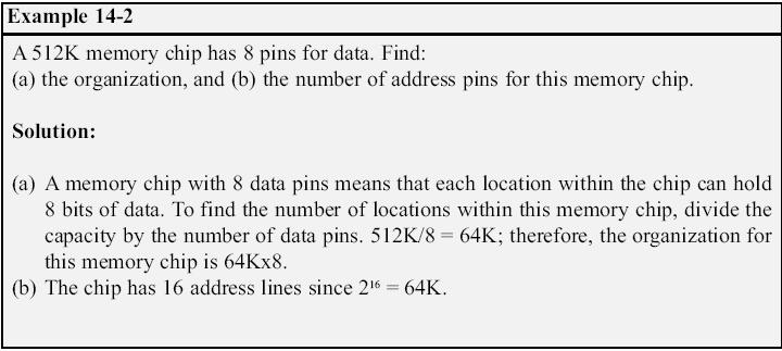
2 Memory Capacity The number of bits that a semiconductor memory chip can store Called chip capacity It can be in units of Kbits (kilobits), Mbits (megabits), and so on This must be distinguished from the storage capacity of computer systems While the memory capacity of a memory IC chip is always given bits, the memory capacity of a computer system is given in bytes 16M memory chip 16 megabits A computer comes with 16M memory 16 megabytes
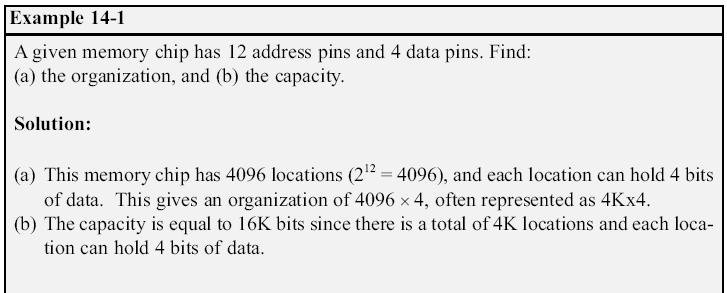
3 Memory Organization Memory chips are organized into a number of locations within the IC Each location can hold 1 bit, 4 bits, 8 bits, or even 16 bits The number of locations within a memory IC depends on the address pins The number of bits that each location can hold is always equal to the number of data pins A memory chip contain 2 x location, where x is the number of address pins Each location contains y bits, where y is the number of data pins on the chip The entire chip will contain 2 x y bits
4 Speed One of the most important characteristics of a memory chip is the speed at which its data can be accessed To access the data, the address is presented to the address pins The READ pin is activated After a certain amount of time has elapsed, the data shows up at the data pins The shorter this elapsed time, the better, and consequently, the more expensive the memory chip The speed of the memory chip is commonly referred to as its access time
5
6 ROM (Read-only Memory) ROM is a type of memory that does not lose its contents when the power is turned off ROM is also called nonvolatile memory There are different types of read-only memory PROM EPROM EEPROM Flash EPROM Mask ROM
7 PROM (Programmable ROM) PROM refers to the kind of ROM that the user can burn information into PROM is a user-programmable memory For every bit of the PROM, there exists a fuse If the information burned into PROM is wrong, that PROM must be discarded since its internal fuses are blown permanently PROM is also referred to as OTP (one-time programmable) Programming ROM, also called burning ROM It requires special equipment called a ROM burner or ROM programmer
8 EPROM (Erasable Programmable ROM) EPROM was invented to allow making changes in the contents of PROM after it is burned In EPROM, one can program the memory chip and erase it thousands of times A widely used EPROM is called UVEPROM UV stands for ultra-violet They have a window that is used to shine ultraviolet (UV) radiation to erase its contents The only problem with UV-EPROM is that erasing its contents can take up to 20 minutes
9 EPROM (Erasable Programmable ROM) (cont.) To program a UV-EPROM chip, the following steps must be taken: Its contents must be erased Removed from its socket on the system board Placed in EPROM erasure equipment to expose it to UV radiation for minutes Program the chip Place it in the ROM burner To burn code or data into EPROM, the ROM burner uses 12.5 volts, Vpp, or higher, depending on the EPROM type Place it back into its system board socket
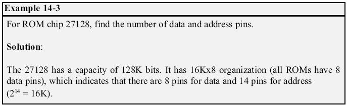
10 EPROM (Erasable Programmable ROM) (cont.) There is an EPROM programmer (burner) There is also separate EPROM erasure equipment The major disadvantage is that it cannot be programmed while in the system board Notice the pattern of the IC numbers Ex refers to UV-EPROM that has a capacity of 128K bits and access time of 250 nanoseconds 27xx always refers to UV-EPROM chips
11
12 EEPROM (Electrically Erasable Programmable ROM) EEPROM has several advantage: Its method of erasure is electrical and instant As opposed to the 20-minute erasure time required for UVEPROM One can select which byte to be erased In contrast to UV-EPROM, in which the entire contents of ROM are erased One can program and erase its contents while it is still in the system board The designer incorporate into the system board the circuitry to program the EEPROM
13 Flash Memory EPROM Flash EPROM has become a popular userprogrammable memory chip since the early 1990s The process of erasure of the entire contents takes less than a second, or might in a flash The erasure method is electrical It is commonly called flash memory The major difference between EEPROM and flash memory is Flash memory s contents are erased, then the entire device is erased
14 Flash Memory EPROM (cont.) There are some flash memories are recently made so that the erasure can be done block by block One can erase a desired section or byte on EEPROM It is believed that flash memory will replace part of the hard disk as a mass storage medium The flash memory can be programmed while it is in its socket on the system board Widely used as a way to upgrade PC BIOS ROM
15 Flash Memory EPROM (cont.) Flash memory is semiconductor memory with access time in the range of 100 ns Compared with disk access time in the range of tens of milliseconds Flash memory s program/erase cycles must become infinite, like hard disks Program/erase cycle refers to the number of times that a chip can be erased and programmed before it becomes unusable The program/erase cycle is 100,000 for flash and EEPROM, 1000 for UV-EPROM
16 RAM (Random Access Memory) RAM memory is called volatile memory Since cutting off the power to the IC will result in the loss of data Sometimes RAM is also referred to as RAWM (read and write memory) In contrast to ROM, which cannot be written to There are three types of RAM Static RAM (SRAM) NV-RAM (nonvolatile RAM) Dynamic RAM (DRAM)
17 SRAM (Static RAM) Storage cells in static RAM memory are made of flip-flops They do not require refreshing in order to keep their data The problem with the use of flip-flops for storage cells is: Each cell require at least 6 transistors to build, and the cell holds only 1 bit of data In recent years, the cells have been made of 4 transistors, given birth to a high-capacity SRAM Still too many Its capacity is far below DRAM
18
19 NV-RAM (Nonvolatile RAM) It combines the best of RAM and ROM The read and write ability of RAM, plus the nonvolatility of ROM NV-RAM chip internally is made of the following components It uses extremely power-efficient SRAM cells built out of CMOS It uses an internal lithium battery as a backup energy source It uses an intelligent control circuitry The main job of this control circuitry is to monitor the Vcc pin constantly to detect loss of the external power supply
20 DRAM (Dynamic RAM) Dynamic RAM uses a capacitor to store each bit It cuts down the number of transistors needed to build the cell It requires constant refreshing due to leakage The advantages and disadvantages: Major advantages are high capacity, cheaper cost per bit, and lower power consumption per bit The disadvantages is It must be refreshed periodically, due to the fact that the capacitor cell loses its charge While it is being refreshed, the data cannot be accessed
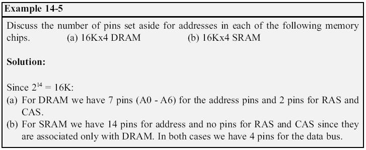
21 Packing Issue in DRAM A problem of packing a large number of cells into a single chip with the normal number of pins assigned to addresses Large number of pins defeats the purpose of high density and small packaging A 64K-bit chip (64K 1) must have 16 address lines and 1 data line, requiring 16 pins to send in address DRAM memory chips can have any of the x1, x4, x8, x16 organizations The method used is to split the address in half To send in each half of the address through the same pins, thereby requiring fewer address pins
22 Packing Issue in DRAM (cont.) Internally, the DRAM structure is divided into a square of rows and columns The first half of the address is called row The second half is called column The first half of the address is sent in through the address pins By activating RAS (row address strobe) The internal latches inside DRAM grab the first half After that, the second half of the address is sent in through the same pins By activating CAS (column address strobe) The internal latches inside DRAM latch the second half
23
24 Memory Address Decoding The CPU provides the address of the data It is the job of the decoding circuitry to locate the selected memory block Memory chips have one or more pins called CS (chip select) Must be activated for the memory s contents to be accessed Sometimes the chip select is also referred to as chip enable (CE) In connecting a memory chip to the CPU, note the following points:
25 Memory Address Decoding (cont.) The data bus of the CPU is connected directly to the data pins of the memory chip Control signals RD (read) and WR (memory write) from the CPU are connected to the OE (output enable) and WE (write enable) pins of the memory chip In the case of the address buses: The lower bits of the address from the CPU go directly to the memory chip address pins The upper ones are used to activate the CS pin of the memory chip
26 Memory Address Decoding (cont.) Memories are divided into blocks The output of the decoder selects a given memory block Using simple logic gates Using the 74LS138 Using programmable logics The simplest way of decoding circuitry is the use of NAND or other gates The output of a NAND gate is active low The CS pin is also active low Makes them a perfect match
27
28 Using 74LS Decoder This is one of the most widely used address decoders The 3 inputs A, B, and C generate 8 active-low outputs Y0 Y7 Each Y output is connected to CS of a memory chip Allowing control of 8 memory blocks by a single 74LS138 A, B, and C select which output is activated There are three additional inputs, G2A, G2B, and G1 G2A and G2B are both active low, and G1 is active high
 If any one of the inputs G1, G2A, or G2B is not connected to an address signal, they must be")
29 Using 74LS Decoder (cont.) If any one of the inputs G1, G2A, or G2B is not connected to an address signal, they must be activated permanently either by V cc or ground Depending on the activation level
30
31
32 Using Programmable Logic Other widely used decoders are programmable logic chips Such as PAL and GAL chips One disadvantage of these chips is that one must have access to a PAL/GAL software and burner The 74LS138 needs neither of these The advantage of these chips is that they are much more versatile since they can be programmed for any combination of address ranges
33 Interfacing External ROM The 8031 chip is a ROMless version of the 8051 It is exactly like any member of the 8051 family as far as executing the instructions and features are concerned It must be connected to external ROM memory containing the program code 8031 is ideal for many systems where the onchip ROM of 8051 is not sufficient Since 8051 allows the program size to be as large as 64K bytes
34 EA Pin For 8751/89C51/DS5000-based system, connect the EA pin to Vcc To indicate that the program code is stored in the microcontroller s on-chip ROM To indicate that the program code is stored in external ROM, EA must be connected to GND
35
36 P0 and P2 in Providing Address 8031/51 is capable of accessing up to 64K bytes of program code Since the PC (program counter) is 16-bit In the 8031/51, port 0 and port 2 provide the 16-bit address to access external memory P0 provides the lower 8 bit address A0 A7 P2 provides the upper 8 bit address A8 A15 P0 is also used to provide the 8-bit data bus D0 D7 P0 is used for both the address and data paths Address/data multiplexing
37 ALE Pin ALE (address latch enable) pin is an output pin for 8031/51 ALE = 0, P0 is used for data path ALE = 1, P0 is used for address path To extract the address from the P0 pins Connect P0 to a 74LS373 Use the ALE pin to latch the address Normally ALE = 0, and P0 is used as a data bus Sending data out or bringing data in To use P0 as an address bus, it puts the addresses A0 A7 on the P0 pins and activates ALE = 1
38
39 PSEN Pin PSEN (program store enable) signal is an output signal for the 8031/51 It must be connected to the OE pin of a ROM containing the program code When the EA pin is connected to GND, the 8031/51 fetches opcode from external ROM by using PSEN In systems based on the 8751/89C51/ DS5000 where EA is connected to Vcc These chips do not activate the PSEN pin The on-chip ROM contains program code
40
41
42 On-Chip and Off-Chip Code ROM In an 8751 (89C51) system we could use on-chip ROM for boot code and an external ROM will contain the user s program We still have EA = Vcc, Upon reset 8051 executes the on-chip program first When it reaches the end of the on-chip ROM, it switches to external ROM for rest of program
43
44
45 Data Memory Space 8051 has 128K bytes of address space 64K bytes are set aside for program code Program space is accessed using the program counter (PC) to locate and fetch instructions We can place data in the code space Used the instruction MOVC to get data, where C stands for code The other 64K bytes are set aside for data The data memory space is accessed using the DPTR register and an instruction called MOVX X stands for external The data memory space must be implemented externally
46 External ROM for Data We use RD to connect the 8031/51 to external ROM containing data For the ROM containing the program code, PSEN is used to fetch the code

47 MOVX Instruction MOVX is a widely used for access to external data memory space To bring externally stored data into the CPU, we use the instruction MOVX A,@DPTR
48
49
50 External Data RAM To connect the 8051 to an external SRAM, we must use both RD (P3.7) and WR (P3.6) In writing data to external data RAM, we use the instruction
51
52
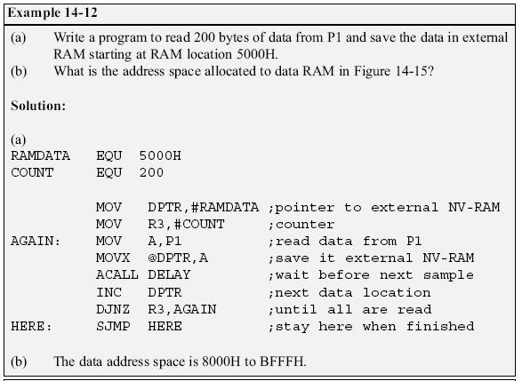
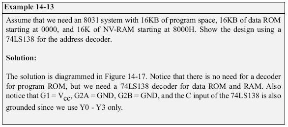
53 Single External ROM for Code and Data An 8031-based system connected to a single 64K 8 (27512) external ROM chip The single external ROM chip is used for both program code and data storage For example, the space FFFH is allocated to program code Address space 8000H FFFFH is set aside for data In accessing the data, we use the MOVX instruction To allow a single ROM chip to provide both program code space and data space, we use an AND gate to signal the OE

54 A 15 64K 8
55
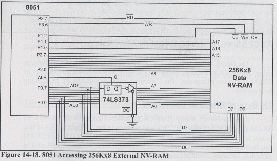
56 Interfacing to Large External Memory In some applications we need a large amount of memory to store data The 8051 can support only 64K bytes of external data memory since DPTR is 16-bit To solve this problem Connect A0 A15 of the 8051 directly to the external memory s A0 A15 pins Use some of the P1 pins to access the 64K bytes blocks inside the single 256K 8 memory chip
57
58
59
Principle and Interface Techniques of Microcontroller
 Principle and Interface Techniques of Microcontroller --8051 Microcontroller and Embedded Systems Using Assembly and C LI, Guang ( 李光 ) Prof. PhD, DIC, MIET WANG, You ( 王酉 ) PhD, MIET 杭州 浙江大学 2015 Chapter
CPEG300 Embedded System Design. Lecture 3 Memory
 CPEG300 Embedded System Design Lecture 3 Memory Hamad Bin Khalifa University, Spring 2018 Review Von Neumann vs. Harvard architecture? System on Board, system on chip? Generic Hardware Architecture of
Chapter TEN. Memory and Memory Interfacing
 Chapter TEN Memory and Memory Interfacing OBJECTIVES this chapter enables the student to: Define the terms capacity, organization, and speed as used in semiconductor memories. Calculate the chip capacity
ORG ; Week8. Memory and Memory Interfacing
 Dec 10 Hex A Bin 00001010 ORG ; Week8 Memory and Memory Interfacing OBJECTIVES this chapter enables the student to: Define the terms capacity, organization, and speed as used in semiconductor memories.
Lecture Objectives. Introduction to Computing Chapter 0. Topics. Numbering Systems 04/09/2017
 Lecture Objectives Introduction to Computing Chapter The AVR microcontroller and embedded systems using assembly and c Students should be able to: Convert between base and. Explain the difference between
Interface DAC to a PC. Control Word of MC1480 DAC (or DAC 808) 8255 Design Example. Engineering 4862 Microprocessors
 8255 Design Example. Engineering 4862 Microprocessors") Interface DAC to a PC Engineering 4862 Microprocessors Lecture 22 Cheng Li EN-4012 licheng@engr.mun.ca DAC (Digital-to-Analog Converter) Device used to convert digital pulses to analog signals Two methods
Interface DAC to a PC Engineering 4862 Microprocessors Lecture 22 Cheng Li EN-4012 licheng@engr.mun.ca DAC (Digital-to-Analog Converter) Device used to convert digital pulses to analog signals Two methods
UNIT 3 THE 8051-REAL WORLD INTERFACING
 UNIT 3 THE 8051-REAL WORLD INTERFACING 8031/51 INTERFACING TO EXTERNAL MEMORY The number of bits that a semiconductor memory chip can store is called chip capacity It can be in units of Kbits (kilobits),
Microcontroller Systems. ELET 3232 Topic 11: General Memory Interfacing
 Microcontroller Systems ELET 3232 Topic 11: General Memory Interfacing 1 Objectives To become familiar with the concepts of memory expansion and the data and address bus To design embedded systems circuits
COMP3221: Microprocessors and. and Embedded Systems. Overview. Lecture 23: Memory Systems (I)
") COMP3221: Microprocessors and Embedded Systems Lecture 23: Memory Systems (I) Overview Memory System Hierarchy RAM, ROM, EPROM, EEPROM and FLASH http://www.cse.unsw.edu.au/~cs3221 Lecturer: Hui Wu Session
COMP3221: Microprocessors and Embedded Systems Lecture 23: Memory Systems (I) Overview Memory System Hierarchy RAM, ROM, EPROM, EEPROM and FLASH http://www.cse.unsw.edu.au/~cs3221 Lecturer: Hui Wu Session
Basic Organization Memory Cell Operation. CSCI 4717 Computer Architecture. ROM Uses. Random Access Memory. Semiconductor Memory Types
 CSCI 4717/5717 Computer Architecture Topic: Internal Memory Details Reading: Stallings, Sections 5.1 & 5.3 Basic Organization Memory Cell Operation Represent two stable/semi-stable states representing
Memory & Simple I/O Interfacing
 Chapter 10 Memory & Simple I/O Interfacing Expected Outcomes Explain the importance of tri-state devices in microprocessor system Distinguish basic type of semiconductor memory and their applications Relate
Concept of Memory. The memory of computer is broadly categories into two categories:
 Concept of Memory We have already mentioned that digital computer works on stored programmed concept introduced by Von Neumann. We use memory to store the information, which includes both program and data.
Semiconductor Memories: RAMs and ROMs
 Semiconductor Memories: RAMs and ROMs Lesson Objectives: In this lesson you will be introduced to: Different memory devices like, RAM, ROM, PROM, EPROM, EEPROM, etc. Different terms like: read, write,
Address connections Data connections Selection connections
 Interface (cont..) We have four common types of memory: Read only memory ( ROM ) Flash memory ( EEPROM ) Static Random access memory ( SARAM ) Dynamic Random access memory ( DRAM ). Pin connections common
Contents. Main Memory Memory access time Memory cycle time. Types of Memory Unit RAM ROM
 Memory Organization Contents Main Memory Memory access time Memory cycle time Types of Memory Unit RAM ROM Memory System Virtual Memory Cache Memory - Associative mapping Direct mapping Set-associative
Unit 6 1.Random Access Memory (RAM) Chapter 3 Combinational Logic Design 2.Programmable Logic
 Chapter 3 Combinational Logic Design 2.Programmable Logic") EE 200: Digital Logic Circuit Design Dr Radwan E Abdel-Aal, COE Unit 6.Random Access Memory (RAM) Chapter 3 Combinational Logic Design 2. Logic Logic and Computer Design Fundamentals Part Implementation
EE 200: Digital Logic Circuit Design Dr Radwan E Abdel-Aal, COE Unit 6.Random Access Memory (RAM) Chapter 3 Combinational Logic Design 2. Logic Logic and Computer Design Fundamentals Part Implementation
Memory Overview. Overview - Memory Types 2/17/16. Curtis Nelson Walla Walla University
 Memory Overview Curtis Nelson Walla Walla University Overview - Memory Types n n n Magnetic tape (used primarily for long term archive) Magnetic disk n Hard disk (File, Directory, Folder) n Floppy disks
Read and Write Cycles
 Read and Write Cycles The read cycle is shown. Figure 41.1a. The RAS and CAS signals are activated one after the other to latch the multiplexed row and column addresses respectively applied at the multiplexed
(Advanced) Computer Organization & Architechture. Prof. Dr. Hasan Hüseyin BALIK (5 th Week)
 Computer Organization & Architechture. Prof. Dr. Hasan Hüseyin BALIK (5 th Week)") + (Advanced) Computer Organization & Architechture Prof. Dr. Hasan Hüseyin BALIK (5 th Week) + Outline 2. The computer system 2.1 A Top-Level View of Computer Function and Interconnection 2.2 Cache Memory
+ (Advanced) Computer Organization & Architechture Prof. Dr. Hasan Hüseyin BALIK (5 th Week) + Outline 2. The computer system 2.1 A Top-Level View of Computer Function and Interconnection 2.2 Cache Memory
William Stallings Computer Organization and Architecture 8th Edition. Chapter 5 Internal Memory
 William Stallings Computer Organization and Architecture 8th Edition Chapter 5 Internal Memory Semiconductor Memory The basic element of a semiconductor memory is the memory cell. Although a variety of
Embedded Systems Design: A Unified Hardware/Software Introduction. Outline. Chapter 5 Memory. Introduction. Memory: basic concepts
 Hardware/Software Introduction Chapter 5 Memory Outline Memory Write Ability and Storage Permanence Common Memory Types Composing Memory Memory Hierarchy and Cache Advanced RAM 1 2 Introduction Memory:
Embedded Systems Design: A Unified Hardware/Software Introduction. Chapter 5 Memory. Outline. Introduction
 Hardware/Software Introduction Chapter 5 Memory 1 Outline Memory Write Ability and Storage Permanence Common Memory Types Composing Memory Memory Hierarchy and Cache Advanced RAM 2 Introduction Embedded
Summer 2003 Lecture 18 07/09/03
 Summer 2003 Lecture 18 07/09/03 NEW HOMEWORK Instruction Execution Times: The 8088 CPU is a synchronous machine that operates at a particular clock frequency. In the case of the original IBM PC, that clock
CREATED BY M BILAL & Arslan Ahmad Shaad Visit:
 CREATED BY M BILAL & Arslan Ahmad Shaad Visit: www.techo786.wordpress.com Q1: Define microprocessor? Short Questions Chapter No 01 Fundamental Concepts Microprocessor is a program-controlled and semiconductor
ET2640. Unit 5:ADVANCED I/O TECHNIQUES Pearson Education, Inc. Pearson Prentice Hall Upper Saddle River, NJ 07458
 ET2640 Unit 5:ADVANCED I/O TECHNIQUES skong@itt-tech.edu HARDWARE CONNECTION CHAPTER 8 8051 PINOUT XTAL1 & XTAL2 On-chip oscillator requires an external clock Quartz crystal clock 2 external 30 pf capacitors
Allmost all systems contain two main types of memory :
 Memory Interface Allmost all systems contain two main types of memory : read-only memory (ROM) system software and permanent system data random access memory (RAM) or read/write memory application software
Grundlagen Microcontroller Memory. Günther Gridling Bettina Weiss
 Grundlagen Microcontroller Memory Günther Gridling Bettina Weiss 1 Lecture Overview Memory Memory Types Address Space Allocation 2 Memory Requirements What do we want to store? program constants (e.g.
Introduction read-only memory random access memory
 Memory Interface Introduction Simple or complex, every microprocessorbased system has a memory system. Almost all systems contain two main types of memory: read-only memory (ROM) and random access memory
Memory Pearson Education, Inc., Hoboken, NJ. All rights reserved.
 1 Memory + 2 Location Internal (e.g. processor registers, cache, main memory) External (e.g. optical disks, magnetic disks, tapes) Capacity Number of words Number of bytes Unit of Transfer Word Block Access
CS 320 February 2, 2018 Ch 5 Memory
 CS 320 February 2, 2018 Ch 5 Memory Main memory often referred to as core by the older generation because core memory was a mainstay of computers until the advent of cheap semi-conductor memory in the
Memory Expansion. Lecture Embedded Systems
 Memory Expansion Lecture 22 22-1 In These Notes... Memory Types Memory Expansion Interfacing Parallel Serial Direct Memory Access controllers 22-2 Memory Characteristics and Issues Volatility - Does it
Memory Interfacing & decoding. Intel CPU s
 Memory Interfacing & decoding in Intel CPU s Outline Address decoding Chip select Memory configurations Minimum Mode - - A19 - A19 - Simplified Drawing of 8088 Minimum Mode MEMORY MEMW When Memory is selected?
Module 5a: Introduction To Memory System (MAIN MEMORY)
") Module 5a: Introduction To Memory System (MAIN MEMORY) R E F E R E N C E S : S T A L L I N G S, C O M P U T E R O R G A N I Z A T I O N A N D A R C H I T E C T U R E M O R R I S M A N O, C O M P U T E
Module 5a: Introduction To Memory System (MAIN MEMORY) R E F E R E N C E S : S T A L L I N G S, C O M P U T E R O R G A N I Z A T I O N A N D A R C H I T E C T U R E M O R R I S M A N O, C O M P U T E
Menu. word size # of words byte = 8 bits
 Menu LSI Components >Random Access Memory (RAM) Static RAM (SRAM) Dynamic RAM (DRAM) Read-Only Memory (ROM) Look into my... See figures from Lam text on web: RAM_ROM_ch6.pdf 1 It can be thought of as 1
EE251: Thursday November 15
 EE251: Thursday November 15 Major new topic: MEMORY A KEY topic HW #7 due today; HW #8 due Thursday, Nov. 29 Lab #8 finishes this week; due week of Nov. 26 All labs MUST be completed/handed-in by Dec.
UMBC. Select. Read. Write. Output/Input-output connection. 1 (Feb. 25, 2002) Four commonly used memories: Address connection ... Dynamic RAM (DRAM)
 Four commonly used memories: Address connection ... Dynamic RAM (DRAM)") Memory Types Two basic types: ROM: Read-only memory RAM: Read-Write memory Four commonly used memories: ROM Flash (EEPROM) Static RAM (SRAM) Dynamic RAM (DRAM) Generic pin configuration: Address connection
Memory Types Two basic types: ROM: Read-only memory RAM: Read-Write memory Four commonly used memories: ROM Flash (EEPROM) Static RAM (SRAM) Dynamic RAM (DRAM) Generic pin configuration: Address connection
UNIT V (PROGRAMMABLE LOGIC DEVICES)
") UNIT V (PROGRAMMABLE LOGIC DEVICES) Introduction There are two types of memories that are used in digital systems: Random-access memory(ram): perform both the write and read operations. Read-only memory(rom):
UNIT V (PROGRAMMABLE LOGIC DEVICES) Introduction There are two types of memories that are used in digital systems: Random-access memory(ram): perform both the write and read operations. Read-only memory(rom):
UNIT-V MEMORY ORGANIZATION
 UNIT-V MEMORY ORGANIZATION 1 The main memory of a computer is semiconductor memory.the main memory unit is basically consists of two kinds of memory: RAM (RWM):Random access memory; which is volatile in
Keywords: NVSRAM, DRAM, SRAM, EEPROM, shadow RAM, NV Memory, MK48Z08, MK48Z18, nvsrams, NV SRAMs
 Maxim > Design Support > Technical Documents > Application Notes > Memory > APP 540 Keywords: NVSRAM, DRAM, SRAM, EEPROM, shadow RAM, NV Memory, MK48Z08, MK48Z18, nvsrams, NV SRAMs APPLICATION NOTE 540
Chapter 5 Internal Memory
 Chapter 5 Internal Memory Memory Type Category Erasure Write Mechanism Volatility Random-access memory (RAM) Read-write memory Electrically, byte-level Electrically Volatile Read-only memory (ROM) Read-only
Lecture-7 Characteristics of Memory: In the broad sense, a microcomputer memory system can be logically divided into three groups: 1) Processor
 Processor") Lecture-7 Characteristics of Memory: In the broad sense, a microcomputer memory system can be logically divided into three groups: 1) Processor memory 2) Primary or main memory 3) Secondary memory Processor
Lecture-7 Characteristics of Memory: In the broad sense, a microcomputer memory system can be logically divided into three groups: 1) Processor memory 2) Primary or main memory 3) Secondary memory Processor
MEMORY BHARAT SCHOOL OF BANKING- VELLORE
 A memory is just like a human brain. It is used to store data and instructions. Computer memory is the storage space in computer where data is to be processed and instructions required for processing are
Lecture 13: Memory and Programmable Logic
 Lecture 13: Memory and Programmable Logic Syed M. Mahmud, Ph.D ECE Department Wayne State University Aby K George, ECE Department, Wayne State University Contents Introduction Random Access Memory Memory
Computer Organization. 8th Edition. Chapter 5 Internal Memory
 William Stallings Computer Organization and Architecture 8th Edition Chapter 5 Internal Memory Semiconductor Memory Types Memory Type Category Erasure Write Mechanism Volatility Random-access memory (RAM)
Logic and Computer Design Fundamentals. Chapter 8 Memory Basics
 Logic and Computer Design Fundamentals Memory Basics Overview Memory definitions Random Access Memory (RAM) Static RAM (SRAM) integrated circuits Arrays of SRAM integrated circuits Dynamic RAM (DRAM) Read
eaymanelshenawy.wordpress.com
 Lectures on Memory Interface Designed and Presented by Dr. Ayman Elshenawy Elsefy Dept. of Systems & Computer Eng.. Al-Azhar University Email : eaymanelshenawy@yahoo.com eaymanelshenawy.wordpress.com Lecture
Computer Organization and Assembly Language (CS-506)
") Computer Organization and Assembly Language (CS-506) Muhammad Zeeshan Haider Ali Lecturer ISP. Multan ali.zeeshan04@gmail.com https://zeeshanaliatisp.wordpress.com/ Lecture 2 Memory Organization and Structure
Computer Organization and Assembly Language (CS-506) Muhammad Zeeshan Haider Ali Lecturer ISP. Multan ali.zeeshan04@gmail.com https://zeeshanaliatisp.wordpress.com/ Lecture 2 Memory Organization and Structure
chapter 8 The Memory System Chapter Objectives
 chapter 8 The Memory System Chapter Objectives In this chapter you will learn about: Basic memory circuits Organization of the main memory Memory technology Direct memory access as an I/O mechanism Cache
ECE 341. Lecture # 16
 ECE 341 Lecture # 16 Instructor: Zeshan Chishti zeshan@ece.pdx.edu November 24, 2014 Portland State University Lecture Topics The Memory System Basic Concepts Semiconductor RAM Memories Organization of
Organization. 5.1 Semiconductor Main Memory. William Stallings Computer Organization and Architecture 6th Edition
 William Stallings Computer Organization and Architecture 6th Edition Chapter 5 Internal Memory 5.1 Semiconductor Main Memory 5.2 Error Correction 5.3 Advanced DRAM Organization 5.1 Semiconductor Main Memory
William Stallings Computer Organization and Architecture 6th Edition. Chapter 5 Internal Memory
 William Stallings Computer Organization and Architecture 6th Edition Chapter 5 Internal Memory Semiconductor Memory Types Semiconductor Memory RAM Misnamed as all semiconductor memory is random access
ECSE-2610 Computer Components & Operations (COCO)
") ECSE-2610 Computer Components & Operations (COCO) Part 18: Random Access Memory 1 Read-Only Memories 2 Why ROM? Program storage Boot ROM for personal computers Complete application storage for embedded
ECSE-2610 Computer Components & Operations (COCO) Part 18: Random Access Memory 1 Read-Only Memories 2 Why ROM? Program storage Boot ROM for personal computers Complete application storage for embedded
Overview. Memory Classification Read-Only Memory (ROM) Random Access Memory (RAM) Functional Behavior of RAM. Implementing Static RAM
 Random Access Memory (RAM) Functional Behavior of RAM. Implementing Static RAM") Memories Overview Memory Classification Read-Only Memory (ROM) Types of ROM PROM, EPROM, E 2 PROM Flash ROMs (Compact Flash, Secure Digital, Memory Stick) Random Access Memory (RAM) Types of RAM Static
Memories Overview Memory Classification Read-Only Memory (ROM) Types of ROM PROM, EPROM, E 2 PROM Flash ROMs (Compact Flash, Secure Digital, Memory Stick) Random Access Memory (RAM) Types of RAM Static
P-2 Digital Design & Applications
 P-2 Digital Design & Applications Semiconductor Memory (Unit-V) By: A K Verma SOS in Electronics & Photonics Pt. Ravishankar Shukla University, Raipur (C.G.) 1 What is Memory? In computing, memory refers
CHAPTER TWELVE - Memory Devices
 CHAPTER TWELVE - Memory Devices 12.1 6x1,024 = 16,384 words; 32 bits/word; 16,384x32 = 524,288 cells 12.2 16,384 addresses; one per word. 12.3 2 16 = 65,536 words = 64K. Thus, memory capacity is 64Kx4.
RISC (Reduced Instruction Set Computer)
") RISC (Reduced Instruction Set Computer) Reduced Instruction Set Computing (RISC), is a microprocessor CPU design philosophy that favors a smaller and simpler set of instructions that all take about the
RISC (Reduced Instruction Set Computer) Reduced Instruction Set Computing (RISC), is a microprocessor CPU design philosophy that favors a smaller and simpler set of instructions that all take about the
UMBC D 7 -D. Even bytes 0. 8 bits FFFFFC FFFFFE. location in addition to any 8-bit location. 1 (Mar. 6, 2002) SX 16-bit Memory Interface
 SX 16-bit Memory Interface") 8086-80386SX 16-bit Memory Interface These machines differ from the 8088/80188 in several ways: The data bus is 16-bits wide. The IO/M pin is replaced with M/IO (8086/80186) and MRDC and MWTC for 80286
8086-80386SX 16-bit Memory Interface These machines differ from the 8088/80188 in several ways: The data bus is 16-bits wide. The IO/M pin is replaced with M/IO (8086/80186) and MRDC and MWTC for 80286
MODULE 12 APPLICATIONS OF MEMORY DEVICES:
 Introduction to Digital Electronic Design, Module 12 Application of Memory Devices 1 MODULE 12 APPLICATIONS OF MEMORY DEVICES: CONCEPT 12-1: REVIEW OF HOW MEMORY DEVICES WORK Memory consists of two parts.
ELCT 912: Advanced Embedded Systems
 Advanced Embedded Systems Lecture 2: Memory and Programmable Logic Dr. Mohamed Abd El Ghany, Memory Random Access Memory (RAM) Can be read and written Static Random Access Memory (SRAM) Data stored so
Read-only memory Implementing logic with ROM Programmable logic devices Implementing logic with PLDs Static hazards
 Points Addressed in this Lecture Lecture 7: ROM Programmable Logic Devices Professor Peter Cheung Department of EEE, Imperial College London Read-only memory Implementing logic with ROM Programmable logic
Large and Fast: Exploiting Memory Hierarchy
 CSE 431: Introduction to Operating Systems Large and Fast: Exploiting Memory Hierarchy Gojko Babić 10/5/018 Memory Hierarchy A computer system contains a hierarchy of storage devices with different costs,
Memory and Programmable Logic
 Memory and Programmable Logic Memory units allow us to store and/or retrieve information Essentially look-up tables Good for storing data, not for function implementation Programmable logic device (PLD),
SECTION-A
 M.Sc(CS) ( First Semester) Examination,2013 Digital Electronics Paper: Fifth ------------------------------------------------------------------------------------- SECTION-A I) An electronics circuit/ device
k -bit address bus n-bit data bus Control lines ( R W, MFC, etc.)
") THE MEMORY SYSTEM SOME BASIC CONCEPTS Maximum size of the Main Memory byte-addressable CPU-Main Memory Connection, Processor MAR MDR k -bit address bus n-bit data bus Memory Up to 2 k addressable locations
THE MEMORY SYSTEM SOME BASIC CONCEPTS Maximum size of the Main Memory byte-addressable CPU-Main Memory Connection, Processor MAR MDR k -bit address bus n-bit data bus Memory Up to 2 k addressable locations
DIGITAL SYSTEM FUNDAMENTALS (ECE421) DIGITAL ELECTRONICS FUNDAMENTAL (ECE422)
 DIGITAL ELECTRONICS FUNDAMENTAL (ECE422)") COURSE / CODE DIGITAL SYSTEM FUNDAMENTALS (ECE421) DIGITAL ELECTRONICS FUNDAMENTAL (ECE422) Memory In computing, memory refers to the computer hardware devices used to store information for immediate use
COURSE / CODE DIGITAL SYSTEM FUNDAMENTALS (ECE421) DIGITAL ELECTRONICS FUNDAMENTAL (ECE422) Memory In computing, memory refers to the computer hardware devices used to store information for immediate use
Computer Structure. Unit 2: Memory and programmable devices
 Computer Structure Unit 2: Memory and programmable devices Translated from Francisco Pérez García (fperez at us.es) by Mª Carmen Romero (mcromerot at us.es, Office G1.51, 954554324) Electronic Technology
Chapter 4 Main Memory
 Chapter 4 Main Memory Course Outcome (CO) - CO2 Describe the architecture and organization of computer systems Program Outcome (PO) PO1 Apply knowledge of mathematics, science and engineering fundamentals
Memory and Programmable Logic
 Memory and Programmable Logic Mano & Ciletti Chapter 7 By Suleyman TOSUN Ankara University Outline RAM Memory decoding Error detection and correction ROM Programmable Logic Array (PLA) Programmable Array
Computer Memory. Textbook: Chapter 1
 Computer Memory Textbook: Chapter 1 ARM Cortex-M4 User Guide (Section 2.2 Memory Model) STM32F4xx Technical Reference Manual: Chapter 2 Memory and Bus Architecture Chapter 3 Flash Memory Chapter 36 Flexible
Chapter 2: Fundamentals of a microprocessor based system
 Chapter 2: Fundamentals of a microprocessor based system Objectives Learn about the basic structure of microprocessor systems Learn about the memory read/write timing diagrams. Learn about address decoding
MEMORY. Computer memory refers to the hardware device that are used to store and access data or programs on a temporary or permanent basis.
 MEMORY Computer memory refers to the hardware device that are used to store and access data or programs on a temporary or permanent basis. There are TWO TYPE of nature of memory in a computer. Temporary/
The Central Processing Unit
 The Central Processing Unit All computers derive from the same basic design, usually referred to as the von Neumann architecture. This concept involves solving a problem by defining a sequence of commands
1. Explain in detail memory classification.[summer-2016, Summer-2015]
![1. Explain in detail memory classification.[summer-2016, Summer-2015]](/thumbs/85/92710493.jpg "1. Explain in detail memory classification.[summer-2016, Summer-2015]") 1. Explain in detail memory classification.[summer-2016, Summer-2015] RAM The memory is a basic component of a microcomputer system. It stores binary instructions and data for the microprocessor. There
1. Explain in detail memory classification.[summer-2016, Summer-2015] RAM The memory is a basic component of a microcomputer system. It stores binary instructions and data for the microprocessor. There
Internal Memory. Computer Architecture. Outline. Memory Hierarchy. Semiconductor Memory Types. Copyright 2000 N. AYDIN. All rights reserved.
 Computer Architecture Prof. Dr. Nizamettin AYDIN naydin@yildiz.edu.tr nizamettinaydin@gmail.com Internal Memory http://www.yildiz.edu.tr/~naydin 1 2 Outline Semiconductor main memory Random Access Memory
CS 265. Computer Architecture. Wei Lu, Ph.D., P.Eng.
 CS 265 Computer Architecture Wei Lu, Ph.D., P.Eng. Part 4: Memory Organization Our goal: understand the basic types of memory in computer understand memory hierarchy and the general process to access memory
a) Memory management unit b) CPU c) PCI d) None of the mentioned
 Memory management unit b) CPU c) PCI d) None of the mentioned") 1. CPU fetches the instruction from memory according to the value of a) program counter b) status register c) instruction register d) program status word 2. Which one of the following is the address generated
1. CPU fetches the instruction from memory according to the value of a) program counter b) status register c) instruction register d) program status word 2. Which one of the following is the address generated
EE 308: Microcontrollers
 EE 308: Microcontrollers AVR Architecture Aly El-Osery Electrical Engineering Department New Mexico Institute of Mining and Technology Socorro, New Mexico, USA January 23, 2018 Aly El-Osery (NMT) EE 308:
Introduction to SRAM. Jasur Hanbaba
 Introduction to SRAM Jasur Hanbaba Outline Memory Arrays SRAM Architecture SRAM Cell Decoders Column Circuitry Non-volatile Memory Manufacturing Flow Memory Arrays Memory Arrays Random Access Memory Serial
7/6/2011. Introduction. Chapter Objectives Upon completion of this chapter, you will be able to:
 Introduction Simple or complex, every microprocessorbased system has a memory system. Almost all systems contain two main types of memory: read-only memory (ROM) and random access memory (RAM) or read/write
Memory Study Material
 Computer memory refers to the devices that are used to store data or programs on a temporary or permanent basis for use in a computer. Any data or instruction entered into the memory of a computer is considered
 Chapter 1 Microprocessor architecture ECE 3120 Dr. Mohamed Mahmoud http://iweb.tntech.edu/mmahmoud/ mmahmoud@tntech.edu Outline 1.1 Computer hardware organization 1.1.1 Number System 1.1.2 Computer hardware
Memory classification:- Topics covered:- types,organization and working
 Memory classification:- Topics covered:- types,organization and working 1 Contents What is Memory? Cache Memory PC Memory Organisation Types 2 Memory what is it? Usually we consider this to be RAM, ROM
M. Sc (CS) (II Semester) Examination, Subject: Computer System Architecture Paper Code: M.Sc-CS-203. Time: Three Hours] [Maximum Marks: 60
![M. Sc (CS) (II Semester) Examination, Subject: Computer System Architecture Paper Code: M.Sc-CS-203. Time: Three Hours] [Maximum Marks: 60](/thumbs/87/96339673.jpg "M. Sc (CS) (II Semester) Examination, Subject: Computer System Architecture Paper Code: M.Sc-CS-203. Time: Three Hours] [Maximum Marks: 60") M. Sc (CS) (II Semester) Examination, 2012-13 Subject: Computer System Architecture Paper Code: M.Sc-CS-203 Time: Three Hours] [Maximum Marks: 60 Note: Question Number 1 is compulsory. Answer any four
M. Sc (CS) (II Semester) Examination, 2012-13 Subject: Computer System Architecture Paper Code: M.Sc-CS-203 Time: Three Hours] [Maximum Marks: 60 Note: Question Number 1 is compulsory. Answer any four
Memory & Logic Array. Lecture # 23 & 24 By : Ali Mustafa
 Memory & Logic Array Lecture # 23 & 24 By : Ali Mustafa Memory Memory unit is a device to which a binary information is transferred for storage. From which information is retrieved when needed. Types of
CS24: INTRODUCTION TO COMPUTING SYSTEMS. Spring 2017 Lecture 13
 CS24: INTRODUCTION TO COMPUTING SYSTEMS Spring 2017 Lecture 13 COMPUTER MEMORY So far, have viewed computer memory in a very simple way Two memory areas in our computer: The register file Small number
COSC 243. Memory and Storage Systems. Lecture 10 Memory and Storage Systems. COSC 243 (Computer Architecture)
") COSC 243 1 Overview This Lecture Source: Chapters 4, 5, and 6 (10 th edition) Next Lecture Control Unit and Microprogramming 2 Electromagnetic Induction Move a magnet through a coil to induce a current
COSC 243 1 Overview This Lecture Source: Chapters 4, 5, and 6 (10 th edition) Next Lecture Control Unit and Microprogramming 2 Electromagnetic Induction Move a magnet through a coil to induce a current
The pin details are given below: V cc, GND = +5V and Ground A 11 -A 0 = address lines. Fig.2.19 Intel 2716 Read Only Memory
 Lecture-8 Typical Memory Chips: In previous lecture, the different types of static memories were discussed. All these memories are random access memories. Any memory location can be accessed in a random
! Memory Overview. ! ROM Memories. ! RAM Memory " SRAM " DRAM. ! This is done because we can build. " large, slow memories OR
 ESE 57: Digital Integrated Circuits and VLSI Fundamentals Lec 2: April 5, 26 Memory Overview, Memory Core Cells Lecture Outline! Memory Overview! ROM Memories! RAM Memory " SRAM " DRAM 2 Memory Overview
Advanced Parallel Architecture Lesson 4 bis. Annalisa Massini /2015
 Advanced Parallel Architecture Lesson 4 bis Annalisa Massini - 2014/2015 Internal Memory RAM Many memory types are random access individual words of memory are directly accessed through wired-in addressing
Sense Amplifiers 6 T Cell. M PC is the precharge transistor whose purpose is to force the latch to operate at the unstable point.
 Announcements (Crude) notes for switching speed example from lecture last week posted. Schedule Final Project demo with TAs. Written project report to include written evaluation section. Send me suggestions
COMP2121: Microprocessors and Interfacing. Introduction to Microprocessors
 COMP2121: Microprocessors and Interfacing Introduction to Microprocessors http://www.cse.unsw.edu.au/~cs2121 Lecturer: Hui Wu Session 2, 2017 1 1 Contents Processor architectures Bus Memory hierarchy 2
DIGITAL SYSTEM FUNDAMENTALS (ECE421) DIGITAL ELECTRONICS FUNDAMENTAL (ECE4220. PROGRAMMABLE LOGIC DEVICES (PLDs)
 DIGITAL ELECTRONICS FUNDAMENTAL (ECE4220. PROGRAMMABLE LOGIC DEVICES (PLDs)") COURSE / CODE DIGITAL SYSTEM FUNDAMENTALS (ECE421) DIGITAL ELECTRONICS FUNDAMENTAL (ECE4220 PROGRAMMABLE LOGIC DEVICES (PLDs) A PLD, or programmable logic device, is an electronic component that is used
COURSE / CODE DIGITAL SYSTEM FUNDAMENTALS (ECE421) DIGITAL ELECTRONICS FUNDAMENTAL (ECE4220 PROGRAMMABLE LOGIC DEVICES (PLDs) A PLD, or programmable logic device, is an electronic component that is used
1. INTRODUCTION TO MICROPROCESSOR AND MICROCOMPUTER ARCHITECTURE:
 1. INTRODUCTION TO MICROPROCESSOR AND MICROCOMPUTER ARCHITECTURE: A microprocessor is a programmable electronics chip that has computing and decision making capabilities similar to central processing unit
+1 (479)
") Memory Courtesy of Dr. Daehyun Lim@WSU, Dr. Harris@HMC, Dr. Shmuel Wimer@BIU and Dr. Choi@PSU http://csce.uark.edu +1 (479) 575-6043 yrpeng@uark.edu Memory Arrays Memory Arrays Random Access Memory Serial
Memory Courtesy of Dr. Daehyun Lim@WSU, Dr. Harris@HMC, Dr. Shmuel Wimer@BIU and Dr. Choi@PSU http://csce.uark.edu +1 (479) 575-6043 yrpeng@uark.edu Memory Arrays Memory Arrays Random Access Memory Serial
The Microcontroller. Lecture Set 3. Major Microcontroller Families. Example Microcontroller Families Cont. Example Microcontroller Families
 The Microcontroller Lecture Set 3 Architecture of the 8051 Microcontroller Microcontrollers can be considered as self-contained systems with a processor, memory and I/O ports. In most cases, all that is
Sir Sadiq s computer notes for class IX. Chapter no 4. Storage Devices
 17 Q: Define Computer memory or storage. Ans: Memory: Memory refers to the place where data is kept for later use. For example, a human being has a memory where he/she stores the things that can be recalled
2. List the five interrupt pins available in INTR, TRAP, RST 7.5, RST 6.5, RST 5.5.
 DHANALAKSHMI COLLEGE OF ENGINEERING DEPARTMENT OF ELECTRICAL AND ELECTRONICS ENGINEERING EE6502- MICROPROCESSORS AND MICROCONTROLLERS UNIT I: 8085 PROCESSOR PART A 1. What is the need for ALE signal in
Computer Systems Organization
 The IAS (von Neumann) Machine Computer Systems Organization Input Output Equipment Stored Program concept Main memory storing programs and data ALU operating on binary data Control unit interpreting instructions
THE MICROCOMPUTER SYSTEM CHAPTER - 2
 THE MICROCOMPUTER SYSTEM CHAPTER - 2 20 2.1 GENERAL ASPECTS The first computer was developed using vacuum tubes. The computers thus developed were clumsy and dissipating more power. After the invention
Sistemas Digitais I LESI - 2º ano
 Sistemas Digitais I LESI - 2º ano Lesson 9 - Memory, CPLDs and FPGAs Prof. João Miguel Fernandes (miguel@di.uminho.pt) Dept. Informática UNIVERSIDADE DO MINHO ESCOLA DE ENGENHARIA - Memory - Any sequential