3. The MC6802 MICROPROCESSOR
|
|
|
- Damon Johnston
- 6 years ago
- Views:
Transcription
1 3. The MC6802 MICROPROCESSOR This chapter provides hardware detail on the Motorola MC6802 microprocessor to enable the reader to use of this microprocessor. It is important to learn the operation and interfacing of the MC6802 microprocessor first. Once you learn MC6802, transition to the other microprocessors (i.e. 6809, 68000, 8080, 8085A, 8086) or to the microcontrollers (i.e. 68HC08, 68HC11, 8051 AT89C51, AT89C52, PIC16F877) manufactured by any of the IC houses is easy. 1
2 3.1 Pin Diagrams and Features Pin Diagrams: Figure 3-1 illustrates the MC6802 microprocessor package and pin diagram. The MC6802 is packaged in 40-pin dual in-line package (DIP). This device operate from a single 5V supply. (V CC =+5V, V SS =0V or GND) Power dissipation of MC6802 is less than 1.5 W. 2

3 FIGURE 3-1 Package and pin diagram of the Motorola MC6802 microprocessor 3
4 Features: 1. On-chip clock circuit x8 bit (128 byte) on-chip RAM (00 to 7FH) bytes of RAM are retainable (00H to 1FH) 4. Software-compatible with the MC Standard TTL-compatible inputs and outputs 6. 8-bit word size bit memory addressing 8. Interrupt capability 4
5 3.2 Bus and Control Signals Proper operation of the MPU requires that certain control and timing signals be provided to accomplish specific functions and the other signal lines be monitored to determine the state of the processor. Busses: Address Bus (A 0..A 15 ), Data Bus (D 0..D 7 ) Bus Control Signals: Enable (E), Valid Memory Address (VMA), Read/Write (R/W) MPU Control Signals: Reset (RESET), Halt (HALT), Interrupt Request (IRQ), Non-Maskable Interrupt (NMI), Memory Ready (MR). 5

6 FIGURE 3-2 Bus and control signals of the MC6802 microprocessor 6
7 1) Address Bus (A0-A15) Sixteen pins are used for the address bus. The outputs are capable of driving one standard TTL load and 90pF. These lines do not have three-state capability. 7
8 2) Data Bus (D0-D7) Eight pins are used for the data bus. It is bidirectional, transferring data to and from the memory and peripheral devices. It also has three-state output buffers capable of driving one standard TTL load and 130 pf. Data bus will be in the output mode when the internal RAM is accessed and RE will be high. This prohibits external data entering the MPU. External RAM at 0000H to 007FH must be disabled when internal RAM is accessed. It should be noted that the internal RAM is fully decoded from 0000H to 007FH. 8
9 3) Halt (HALT) When this input is in the low state, all activity in the machine will be halted. This input is level sensitive. In the HALT mode, the machine will stop at the end of an instruction, bus available will be at a high state (BA=1), valid memory address will be at a low state (VMA=0). The address bus will display the address of the next instruction. HALT should be tied high if not used. 9
10 4) Read/Write (R/W) This TTL-compatible output signals indicate to the peripherals and memory devices that whether the MPU is in a read (high) or write (low) state. The normal standby state of this signal is read (high). When the processor is halted, it will be in the read state. This output is capable of driving one standard TTL load and 90 pf. 10
11 5) Valid Memory Address (VMA) This output indicates to peripheral devices that there is a valid address on the address bus. In normal operation, this signal should be utilized for enabling peripheral interfaces such as the PIA (6821) and ACIA (6850). This signal is not three-state. One standard TTL load and 90 pf may be directly driven by this active high signal. 11
12 6) Bus Available (BA) The bus available signal will normally be in the low state; when activated, it will go to the high state indicating that the microprocessor has stopped and that the address bus is available (but not in a three-state condition). This will occur if the HALT line is in the low state or the processor is in the WAIT state as a result of the execution of a WAIT instruction. At such time, all three-state output drivers will go to their off-state and other outputs to their normally inactive level. The processor is removed from the WAIT state by the occurrence of a maskable (mask bit I=0) or nonmaskable interrupts. This output is capable of driving one standard TTL load and 30 pf. 12
13 7) Ram Enable (RE) A TTL compatible RAM enable input controls the on-chip RAM of the MC When placed in the high state, the on-chip memory is enabled to respond to the MPU controls. In the low state, RAM is disabled. 13
14 8) Enable (E) This signal is used to enable the memory or I/O device. This pin supplies the clock for the MPU and the rest of the system. This is a single phase TTL-compatible clock. This clock may be conditioned by a memory read signal. This output is capable of driving one standard TTL load and 130 pf. 14
15 The MC6802 Bus Timing
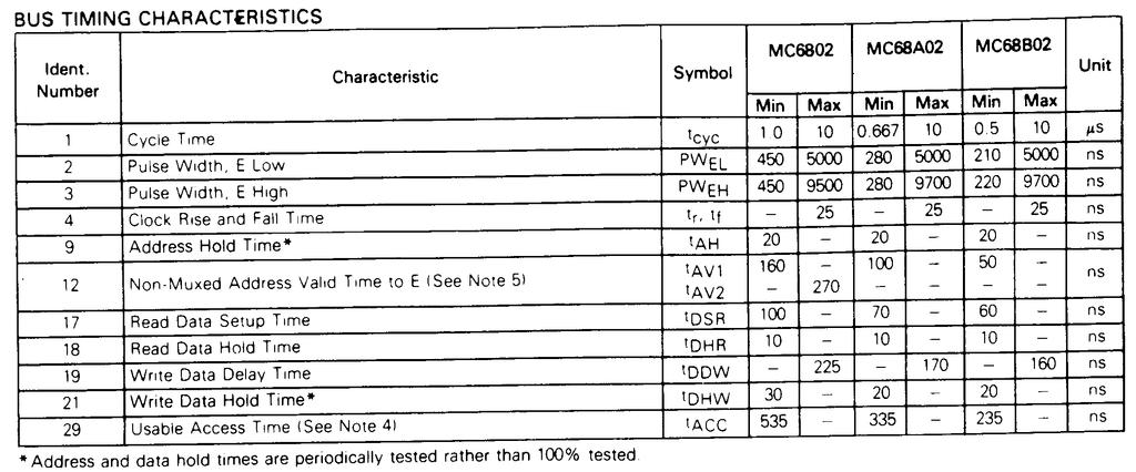
16 16
17 17
18 9) Crystal Connection Inputs (EXTAL, XTAL) These inputs are used for the internal oscillator that may be crystal controlled. These connections are for a parallel resonant fundamental crystal (see figure 3-3). A divide-by-four circuit has been added so a 4 MHz crystal may be used in lieu of a 1 MHz crystal for a most cost-effective system. 18
19 FIGURE 3-3 Crystal specifications 19
20 10) Memory Ready (MR) MR is a TTL-compatible input signal controlling the stretching of E. When MR is high, E will be in normal operation. When MR is low, E will be stretched integral numbers of half periods, thus allowing interface to slow memories. MR should be tied high (connected directly to V CC ) if not used. 20
21 11) V CC Standby This pin supplies the dc voltage to the first 32 bytes of RAM as well as the RAM Enable (RE) control logic. Thus, retention of data in this portion of the RAM on a power-up, powerdown, or standby condition is guaranteed. 21
22 12) Interrupt Request (IRQ) A low level on this input requests that an interrupt sequence be generated within the machine. The processor will wait until it completes the current instruction at is being executed before it recognizes the request. At that time, if the interrupt mask bit in the condition code register is not set (I=0), the machine will begin an interrupt sequence. 22
23 IRQ sequences: 1) The index register (X), program counter (PC), accumulators (A, B) and condition code register (CCR) are stored away on the stack. 2) Next the MPU will respond to the interrupt request by setting the interrupt mask bit high (I=1) so that no further interrupts may occur. 3) At the end of the cycle, a 16-bit vectoring address, which is located in memory locations FFF8H and FFF9H is loaded which causes the MPU to branch to an interrupt routine in memory. 23
24 NOTEs: 1) The HALT line must be in the high state for interrupts to be serviced. 2) Interrupts will be latched internally while HALT is low. 3) A nominal 3 k (or 3.3k standard ) pullup resistor to V CC should be used for wire-or and optimum control of interrupts. 4) IRQ may be tied directly to V CC If not used. 24
25 13) Reset (RESET) This input is used to reset and start the MPU from a power-down condition, resulting from a power failure or an initial start-up of the processor. When this line is low, the MPU is inactive and the information in the registers will be lost. If a high level is detected on the input, this will signal the MPU to begin the restart sequence. This will start execution of a routine to initialize the processor from its reset condition. 25
26 NOTEs: 1) All the higher order address lines will be forced high. 2) For the restart, the last two (FFFEH, FFFFH) locations in memory will be used to load the program that is addressed by the program counter. 3) During the restart routine, the interrupt mask bit in the Conditon Code Register (CCR) is set (I=1) and must be reset (I=0) before the MPU can be interrupted by (IRQ). Power-up and reset timing are shown in figure
27 Figure 3-4 Power-up and reset timing 27
28 14) Non-Maskable Interrupt (NMI) A low-going edge on this input requests that a non-maskable interrupt sequence be generated within the processor. As with the interrupt request signal, the processor will complete the current instruction that, is being executed before it recognizes the NMI signal. The interrupt mask bit in the condition code register has no effect on the NMI. 28
29 The index register (X), program counter (PC), accumulators (A, B), and condition code registers (CCR) are stored away on the stack. At the end of the cycle, a 16-bit vectoring address which is located in memory locations FFFCH and FFFDH is loaded causing the MPU to branch to an interrupt service routine in memory. A nominal 3 k pullup resistor to VCC should be used for wire-or and optimum control of interrupts. NMI may be tied directly to VCC if not used. 29
30 Inputs IRQ and NMI are hardware interrupt lines that are sampled when E is high (E=1) and will start the interrupt routine on a low E (E=0) following the completion of an instruction. Figure 3-5 is a flowchart describing the major decision paths and interrupt vectors of the microprocessor. 30
31 Figure 3-5 Flowchart and vector table of the MC6802 MPU 31
2. List the five interrupt pins available in INTR, TRAP, RST 7.5, RST 6.5, RST 5.5.
 DHANALAKSHMI COLLEGE OF ENGINEERING DEPARTMENT OF ELECTRICAL AND ELECTRONICS ENGINEERING EE6502- MICROPROCESSORS AND MICROCONTROLLERS UNIT I: 8085 PROCESSOR PART A 1. What is the need for ALE signal in
Pin Description, Status & Control Signals of 8085 Microprocessor
 Pin Description, Status & Control Signals of 8085 Microprocessor 1 Intel 8085 CPU Block Diagram 2 The 8085 Block Diagram Registers hold temporary data. Instruction register (IR) holds the currently executing
1. Internal Architecture of 8085 Microprocessor
 1. Internal Architecture of 8085 Microprocessor Control Unit Generates signals within up to carry out the instruction, which has been decoded. In reality causes certain connections between blocks of the
Pin diagram Common SignalS Architecture: Sub: 8086 HARDWARE
 1 CHAPTER 6 HARDWARE ARCHITECTURE OF 8086 8086 Architecture: 6.1 8086 Pin diagram 8086 is a 40 pin DIP using CHMOS technology. It has 2 GND s as circuit complexity demands a large amount of current flowing
Instructions Involve a Segment Register (SR-field)
") BYTE 1 = 11000111 2 = C7 16 BYTE 2 = (MOD)000(R/M) = 100000112 = 83 16 BYTE 3 = 34 16 and BYTE 4 = 12 16 BYTE 5 = CD 16 and BYTE 6 = AB 16 The machine code for the instruction is: MOV [BP+DI+1234H], 0ABCDH
BYTE 1 = 11000111 2 = C7 16 BYTE 2 = (MOD)000(R/M) = 100000112 = 83 16 BYTE 3 = 34 16 and BYTE 4 = 12 16 BYTE 5 = CD 16 and BYTE 6 = AB 16 The machine code for the instruction is: MOV [BP+DI+1234H], 0ABCDH
1. INTRODUCTION TO MICROPROCESSOR AND MICROCOMPUTER ARCHITECTURE:
 1. INTRODUCTION TO MICROPROCESSOR AND MICROCOMPUTER ARCHITECTURE: A microprocessor is a programmable electronics chip that has computing and decision making capabilities similar to central processing unit
Control Unit: The control unit provides the necessary timing and control Microprocessor resembles a CPU exactly.
 Unit I 8085 and 8086 PROCESSOR Introduction to microprocessor A microprocessor is a clock-driven semiconductor device consisting of electronic logic circuits manufactured by using either a large-scale
MICROPROCESSOR MICROPROCESSOR. From the above description, we can draw the following block diagram to represent a microprocessor based system: Output
 8085 SATISH CHANDRA What is a Microprocessor? The word comes from the combination micro and processor. Processor means a device that processes whatever. In this context, processor means a device that processes
1 MALP ( ) Unit-1. (1) Draw and explain the internal architecture of 8085.
 Unit-1. (1) Draw and explain the internal architecture of 8085.") (1) Draw and explain the internal architecture of 8085. The architecture of 8085 Microprocessor is shown in figure given below. The internal architecture of 8085 includes following section ALU-Arithmetic
(1) Draw and explain the internal architecture of 8085. The architecture of 8085 Microprocessor is shown in figure given below. The internal architecture of 8085 includes following section ALU-Arithmetic
Mechatronics and Measurement. Lecturer:Dung-An Wang Lecture 6
 Mechatronics and Measurement Lecturer:Dung-An Wang Lecture 6 Lecture outline Reading:Ch7 of text Today s lecture: Microcontroller 2 7.1 MICROPROCESSORS Hardware solution: consists of a selection of specific
Chapter 8 Summary: The 8086 Microprocessor and its Memory and Input/Output Interface
 Chapter 8 Summary: The 8086 Microprocessor and its Memory and Input/Output Interface Figure 1-5 Intel Corporation s 8086 Microprocessor. The 8086, announced in 1978, was the first 16-bit microprocessor
BL24C02/BL24C04/BL24C08/BL24C16
 BL24C02/BL24C04/BL24C08/BL24C16 2K bits (256 X 8) / 4K bits (512 X 8) / 8K bits (1024 X 8) / 16K bits (2048 X 8) Two-wire Serial EEPROM Features Two-wire Serial Interface VCC = 1.8V to 5.5V Bi-directional
Chapter 1: Basics of Microprocessor [08 M]
![Chapter 1: Basics of Microprocessor [08 M]](/thumbs/77/75860546.jpg "Chapter 1: Basics of Microprocessor [08 M]") Microprocessor: Chapter 1: Basics of Microprocessor [08 M] It is a semiconductor device consisting of electronic logic circuits manufactured by using either a Large scale (LSI) or Very Large Scale (VLSI)
Microprocessor: Chapter 1: Basics of Microprocessor [08 M] It is a semiconductor device consisting of electronic logic circuits manufactured by using either a Large scale (LSI) or Very Large Scale (VLSI)
Understanding the basic building blocks of a microcontroller device in general. Knows the terminologies like embedded and external memory devices,
 Understanding the basic building blocks of a microcontroller device in general. Knows the terminologies like embedded and external memory devices, CISC and RISC processors etc. Knows the architecture and
MICROPROCESSOR AND MICROCONTROLLER BASED SYSTEMS
 MICROPROCESSOR AND MICROCONTROLLER BASED SYSTEMS UNIT I INTRODUCTION TO 8085 8085 Microprocessor - Architecture and its operation, Concept of instruction execution and timing diagrams, fundamentals of
Z Z-280 MT8930, MT8992/3/4/5 MT8880 MT8888 MT8889 MT8980/1 MT8985, MT8986 (DIP-40) MT8986 (PLCC-44) MT8920B MT8952B
 MT8986 (PLCC-44) MT8920B MT8952B") MSAN-145 How to Interface Mitel Components to Parallel Bus CPUs TABL OF CONTNTS Introduction ISSU 1 August 1993 1.0 Group 1 Components 1.1 Interfacing to the 6802 1.2 Interfacing to the 6809 1.3 Interfacing
MSAN-145 How to Interface Mitel Components to Parallel Bus CPUs TABL OF CONTNTS Introduction ISSU 1 August 1993 1.0 Group 1 Components 1.1 Interfacing to the 6802 1.2 Interfacing to the 6809 1.3 Interfacing
EC 6504 Microprocessor and Microcontroller. Unit II System Bus Structure
 EC 6504 Microprocessor and Microcontroller Unit II 8086 System Bus Structure Syllabus: 8086 Signals Basic Configurations System bus timing System Design using 8086 IO Programming Introduction to multiprogramming
Roberto Muscedere Images and Text Portions 2003 Prentice Hall 1
 Microcomputer Structure and Operation Chapter 5 A Microprocessor ( P) contains the controller, ALU and internal registers A Microcomputer ( C) contains a microprocessor, memory (RAM, ROM, etc), input and
8086 Hardware Specification
 Content: Segment 5 8086 Hardware Specification 8086 Modes of operation. Pin diagram and pin function of 8086. 8284A Clock generator operation and pin functions. Prepared By: Mohammed Abdul Kader Lecturer,
Module Introduction. PURPOSE: The intent of this module is to explain MCU processing of reset and interrupt exception events.
 Module Introduction PURPOSE: The intent of this module is to explain MCU processing of reset and interrupt exception events. OBJECTIVES: - Describe the difference between resets and interrupts. - Identify
EEE3410 Microcontroller Applications Department of Electrical Engineering Lecture 4 The 8051 Architecture
 Department of Electrical Engineering Lecture 4 The 8051 Architecture 1 In this Lecture Overview General physical & operational features Block diagram Pin assignments Logic symbol Hardware description Pin
MicroProcessor. MicroProcessor. MicroProcessor. MicroProcessor
 1 2 A microprocessor is a single, very-large-scale-integration (VLSI) chip that contains many digital circuits that perform arithmetic, logic, communication, and control functions. When a microprocessor
Basic I/O Interface
 Basic I/O Interface - 8255 11 3 THE PROGRAMMABLE PERIPHERAL 82C55 programmable peripheral interface (PPI) is a popular, low-cost interface component found in many applications. The PPI has 24 pins for
MOS INTEGRATED CIRCUIT
 DATA SHEET MOS INTEGRATED CIRCUIT µpd6708 IEBus (Inter Equipment Bus ) PROTOCOL CONTROL LSI DESCRIPTION The µpd6708 is a peripheral LSI for microcontrollers that controls the protocol of the IEBus. This
How to Implement I 2 C Serial Communication Using Intel MCS-51 Microcontrollers
 APPLICATION NOTE How to Implement I 2 C Serial Communication Using Intel MCS-51 Microcontrollers SABRINA D QUARLES APPLICATIONS ENGINEER April 1993 Order Number 272319-001 Information in this document
Lecture Note On Microprocessor and Microcontroller Theory and Applications
 Lecture Note On Microprocessor and Microcontroller Theory and Applications MODULE: 1 1. INTRODUCTION TO MICROPROCESSOR AND MICROCOMPUTER ARCHITECTURE: A microprocessor is a programmable electronics chip
W25X40CL 2.5/3/3.3 V 4M-BIT SERIAL FLASH MEMORY WITH 4KB SECTORS AND DUAL I/O SPI. Publication Release Date: October 15, Revision E
 2.5/3/3.3 V 4M-BIT SERIAL FLASH MEMORY WITH 4KB SECTORS AND DUAL I/O SPI - 1 - Revision E Table of Contents 1. GENERAL DESCRIPTION... 4 2. FEATURES... 4 3. PIN CONFIGURATION SOIC 208-MIL, SOIC 150-MIL
SECTION 5 RESETS AND INTERRUPTS
 SECTION RESETS AND INTERRUPTS Resets and interrupt operations load the program counter with a vector that points to a new location from which instructions are to be fetched. A reset immediately stops execution
AT89S4D12. 8-Bit Microcontroller with 132K Bytes Flash Data Memory AT89S4D12. Features. Description. Pin Configurations
 Features Compatible with MCS-51 Products 128K Bytes of In-System Reprogrammable Flash data memory and 4K Bytes of Downloadable Flash Program Memory Endurance: 1,000 Write/Erase Cycles per Sector Data Retention:
PIN DIAGRAM. Richa Upadhyay Prabhu. NMIMS s MPSTME January 19, 2016
 PIN DIAGRAM Richa Upadhyay Prabhu NMIMS s MPSTME richa.upadhyay@nmims.edu January 19, 2016 Richa Upadhyay Prabhu (MPSTME) 8080 Microprocessor January 19, 2016 1 / 51 Pin Diagram of 8086 Richa Upadhyay
Uniform Sector Dual and Quad Serial Flash GD25Q64B DATASHEET
 DATASHEET 1 Contents 1. FEATURES... 4 2. GENERAL DESCRIPTION... 5 3. MEMORY ORGANIZATION... 7 4. DEVICE OPERATION... 8 5. DATA PROTECTION... 9 6. STATUS REGISTER... 11 7. COMMANDS DESCRIPTION... 13 7.1.
Digital IP Cell 8-bit Microcontroller PE80
 1. Description The is a Z80 compliant processor soft-macro - IP block that can be implemented in digital or mixed signal ASIC designs. The Z80 and its derivatives and clones make up one of the most commonly
8051 Microcontroller
 8051 Microcontroller The 8051, Motorola and PIC families are the 3 leading sellers in the microcontroller market. The 8051 microcontroller was originally developed by Intel in the late 1970 s. Today many
CHAPTER 1 MICROCOMPUTER SYSTEMS. 1.1 Introduction. 1.2 Microcontroller Evolution
 CHAPTER 1 MICROCOMPUTER SYSTEMS 1.1 Introduction The term microcomputer is used to describe a system that includes a microprocessor, program memory, data memory, and an input/output (I/O). Some microcomputer
AT24C01A/02/04/08/16. 2-Wire Serial CMOS E 2 PROM. Features. Description. Pin Configurations. 1K (128 x 8) 2K (256 x 8) 4K (512 x 8) 8K (1024 x 8)
 2K (256 x 8) 4K (512 x 8) 8K (1024 x 8)") AT24C01A/02/04/08/16 Features Low Voltage and Standard Voltage Operation 5.0 (V CC = 4.5V to 5.5V) 2.7 (V CC = 2.7V to 5.5V) 2.5 (V CC = 2.5V to 5.5V) 1.8 (V CC = 1.8V to 5.5V) Internally Organized 128
AT24C01A/02/04/08/16 Features Low Voltage and Standard Voltage Operation 5.0 (V CC = 4.5V to 5.5V) 2.7 (V CC = 2.7V to 5.5V) 2.5 (V CC = 2.5V to 5.5V) 1.8 (V CC = 1.8V to 5.5V) Internally Organized 128
CPE/EE 421/521 Fall 2004 Chapter 4 The CPU Hardware Model. Dr. Rhonda Kay Gaede UAH. The CPU Hardware Model - Overview
 CPE/EE 421/521 Fall 2004 Chapter 4 The 68000 CPU Hardware Model Dr. Rhonda Kay Gaede UAH Fall 2004 1 The 68000 CPU Hardware Model - Overview 68000 interface Timing diagram Minimal configuration using the
DS1845 Dual NV Potentiometer and Memory
 www.maxim-ic.com FEATURES Two linear taper potentiometers -010 one 10k, 100 position & one 10k, 256 position -050 one 10k, 100 position & one 50k, 256 postition -100 one 10k, 100 position & one 100k, 256
Z8 Low Voltage ROM MCUs with Infrared Timers
 Z8 Low Voltage ROM MCUs with Infrared Timers PS021410-0605 ZiLOG Worldwide Headquarters 532 Race Street San Jose, CA 95126-3432 Telephone: 408.558.8500 Fax: 408.558.8300 www.zilog.com This publication
8-bit Microcontroller with 8K Bytes In-System Programmable Flash AT89S52
 Features Compatible with MCS -51 Products 8K Bytes of In-System Programmable (ISP) Flash Memory Endurance: 10,000 Write/Erase Cycles 4.0V to 5.5V Operating Range Fully Static Operation: 0 Hz to 33 MHz
UMBC. 80C86/80C88: CMOS version draws 10mA with temp spec -40 to 225degF. 450mV while input max can be no higher than 800mV). 0 0.
. 0 0.") 8086/88 Device Specifications Both are packaged in DIP (Dual In-Line Packages). 8086: 16-bit microprocessor with a 16-bit data bus 8088: 16-bit microprocessor with an 8-bit data bus. Both are 5V parts:
8086/88 Device Specifications Both are packaged in DIP (Dual In-Line Packages). 8086: 16-bit microprocessor with a 16-bit data bus 8088: 16-bit microprocessor with an 8-bit data bus. Both are 5V parts:
W25X05CL/10CL/20CL 2.5 / 3 / 3.3 V 512K / 1M / 2M-BIT SERIAL FLASH MEMORY WITH 4KB SECTORS AND DUAL I/O SPI
 2.5 / 3 / 3.3 V 512K / 1M / 2M-BIT SERIAL FLASH MEMORY WITH 4KB SECTORS AND DUAL I/O SPI - 1 - Revision B Table of Contents 1. GENERAL DESCRIPTION...4 2. FEATURES...4 3. PIN CONFIGURATION SOIC 150-MIL,
8051 Microcontroller
 8051 Microcontroller 1 Salient Features (1). 8 bit microcontroller originally developed by Intel in 1980. (2). High-performance CMOS Technology. (3). Contains Total 40 pins. (4). Address bus is of 16 bit
MC68HC05J1A/D Rev. 1.0 HC 5 MC68HC05J1A MC68HCL05J1A MC68HSC05J1A. HCMOS Microcontroller Units TECHNICAL DATA
 MC68HC0J1A/D Rev. 1.0 HC MC68HC0J1A MC68HCL0J1A MC68HSC0J1A HCMOS Microcontroller Units TECHNICAL DATA Technical Data Motorola reserves the right to make changes without further notice to any products
History and Basic Processor Architecture
 History and Basic Processor Architecture History of Computers Module 1 Section 1 What Is a Computer? An electronic machine, operating under the control of instructions stored in its own memory, that can
Uniform Sector Dual and Quad Serial Flash GD25Q80B DATASHEET
 DATASHEET 1 Contents 1. FEATURES... 4 2. GENERAL DESCRIPTION... 5 3. MEMORY ORGANIZATION... 7 4. DEVICE OPERATION... 8 5. DATA PROTECTION... 9 6. STATUS REGISTER... 11 7. COMMANDS DESCRIPTION... 13 7.1.
6 Direct Memory Access (DMA)
") 1 License: http://creativecommons.org/licenses/by-nc-nd/3.0/ 6 Direct Access (DMA) DMA technique is used to transfer large volumes of data between I/O interfaces and the memory. Example: Disk drive controllers,
1 License: http://creativecommons.org/licenses/by-nc-nd/3.0/ 6 Direct Access (DMA) DMA technique is used to transfer large volumes of data between I/O interfaces and the memory. Example: Disk drive controllers,
POD 51EH C505L XH0 XH1 XH2 XH3 XH4 XH5 XH6 XH7 XL7 XL6 XL5 XL4 XL3 XL2 XL1 XL0. Figure 1. POD 51EH C505L 20
 6 7.. P P POD 5EH C505L 0 RST R PWD Y IDL Y EML G MON Y MERR R JP T JP0 JP7 ANB FLF EMUL XH0 XH XH XH XH4 XH5 XH6 XH7 XL7 XL6 XL5 XL4 XL XL XL XL0 T XS GSL T MCU RSL T XS T P P4 5 4 0 7 6 5 4 0 NOHAU Corporation
24C08/24C16. Two-Wire Serial EEPROM. Preliminary datasheet 8K (1024 X 8)/16K (2048 X 8) General Description. Pin Configuration
/16K (2048 X 8) General Description. Pin Configuration") Two-Wire Serial EEPROM Preliminary datasheet 8K (1024 X 8)/16K (2048 X 8) Low-voltage Operation 1.8 (VCC = 1.8V to 5.5V) Operating Ambient Temperature: -40 C to +85 C Internally Organized 1024 X 8 (8K),
Two-Wire Serial EEPROM Preliminary datasheet 8K (1024 X 8)/16K (2048 X 8) Low-voltage Operation 1.8 (VCC = 1.8V to 5.5V) Operating Ambient Temperature: -40 C to +85 C Internally Organized 1024 X 8 (8K),
DS1305EN. Serial Alarm Real-Time Clock
 Serial Alarm Real-Time Clock www.maxim-ic.com FEATURES Real-time clock (RTC) counts seconds, minutes, hours, date of the month, month, day of the week, and year with leap-year compensation valid up to
DS1306. Serial Alarm Real Time Clock (RTC)
") www.dalsemi.com FEATURES Real time clock counts seconds, minutes, hours, date of the month, month, day of the week, and year with leap year compensation valid up to 2100 96-byte nonvolatile RAM for data
www.dalsemi.com FEATURES Real time clock counts seconds, minutes, hours, date of the month, month, day of the week, and year with leap year compensation valid up to 2100 96-byte nonvolatile RAM for data
Types of Interrupts:
 Interrupt structure Introduction Interrupt is signals send by an external device to the processor, to request the processor to perform a particular task or work. Mainly in the microprocessor based system
S25FL204K. 4-Mbit 3.0V Serial Flash Memory with Uniform 4 kb Sectors. Data Sheet
 S25FL204K 4-Mbit 3.0V Serial Flash Memory with Uniform 4 kb Sectors Data S25FL204K Cover Notice to Readers: This document states the current technical specifications regarding the Spansion product(s) described
These three counters can be programmed for either binary or BCD count.
 S5 KTU 1 PROGRAMMABLE TIMER 8254/8253 The Intel 8253 and 8254 are Programmable Interval Timers (PTIs) designed for microprocessors to perform timing and counting functions using three 16-bit registers.
ST78C34 GENERAL PURPOSE PARALLEL PRINTER PORT WITH 83 BYTE FIFO DESCRIPTION. PLCC Package FEATURES ORDERING INFORMATION
 GENERAL PURPOSE PARALLEL PRINTER PORT WITH 83 BYTE FIFO DESCRIPTION The ST78C34 is a monolithic Bidirectional Parallel port designed to operate as a general purpose I/O port. It contains all the necessary
Microprocessors and Microcontrollers (EE-231)
") Microprocessors and Microcontrollers (EE-231) Main Objectives 8088 and 80188 8-bit Memory Interface 8086 t0 80386SX 16-bit Memory Interface I/O Interfacing I/O Address Decoding More on Address Decoding
Microprocessors and Microcontrollers (EE-231) Main Objectives 8088 and 80188 8-bit Memory Interface 8086 t0 80386SX 16-bit Memory Interface I/O Interfacing I/O Address Decoding More on Address Decoding
EXPERIMENT #7 PARALLEL INTERFACING USING THE PERIPHERAL INTERFACE ADAPTER (PIA)
") EXPERIMENT #7 PARALLEL INTERFACING USING THE PERIPHERAL INTERFACE ADAPTER (PIA) 1.0 Procedure The purpose of this experiment is to introduce the student to the following topics: the Peripheral Interface
EXPERIMENT #7 PARALLEL INTERFACING USING THE PERIPHERAL INTERFACE ADAPTER (PIA) 1.0 Procedure The purpose of this experiment is to introduce the student to the following topics: the Peripheral Interface
CEIBO FE-5111 Development System
 CEIBO FE-5111 Development System Development System for Atmel W&M T89C5111 Microcontrollers FEATURES Emulates Atmel W&M T89C5111 4K Code Memory Real-Time Emulation and Trace Frequency up to 33MHz/5V ISP
e-pg Pathshala Subject : Computer Science Paper: Embedded System Module: 8051 Architecture Module No: CS/ES/5 Quadrant 1 e-text
 e-pg Pathshala Subject : Computer Science Paper: Embedded System Module: 8051 Architecture Module No: CS/ES/5 Quadrant 1 e-text In this lecture the detailed architecture of 8051 controller, register bank,
DSP56002 PIN DESCRIPTIONS
 nc. SECTION 2 DSP56002 PIN DESCRIPTIONS MOTOROLA 2-1 nc. SECTION CONTENTS 2.1 INTRODUCTION............................................. 2-3 2.2 SIGNAL DESCRIPTIONS......................................
MICROPROCESSOR B.Tech. th ECE
 MICROPROCESSOR B.Tech. th ECE Submitted by: Er. Amita Sharma Dept. of ECE 11/24/2014 2 Microprocessor Architecture The microprocessor can be programmed to perform functions on given data by writing specific
SH69P48A EVB. Application Notes for SH69P48A EVB SH69V48A JP2 J4(ICE_J4) S1 IDD TEST JP1 74HC273 JP4 JP3 74HC273 JP6 STKOVE JP7 SW1 J5(ICE_J5)
 S1 IDD TEST JP1 74HC273 JP4 JP3 74HC273 JP6 STKOVE JP7 SW1 J5(ICE_J5)") SH69P48A EVB Application Notes for SH69P48A EVB The SH69P48A EVB is used to evaluate the SH69P48A chip's function for the development of application program. It contains of a SH69V48A chip to evaluate
SH69P48A EVB Application Notes for SH69P48A EVB The SH69P48A EVB is used to evaluate the SH69P48A chip's function for the development of application program. It contains of a SH69V48A chip to evaluate
Question Bank Microprocessor and Microcontroller
 QUESTION BANK - 2 PART A 1. What is cycle stealing? (K1-CO3) During any given bus cycle, one of the system components connected to the system bus is given control of the bus. This component is said to
Computer Hardware Requirements for ERTSs: Microprocessors & Microcontrollers
 Lecture (4) Computer Hardware Requirements for ERTSs: Microprocessors & Microcontrollers Prof. Kasim M. Al-Aubidy Philadelphia University-Jordan DERTS-MSc, 2015 Prof. Kasim Al-Aubidy 1 Lecture Outline:
DS1846 NV Tri-Potentiometer, Memory, and MicroMonitor
 www.maxim-ic.com FEATURES Three linear taper potentiometers Two 10k, 100-position One 100k, 256-position 248 bytes of user EEPROM memory Monitors microprocessor power supply, voltage sense, and external
Z8 Pod Adapter. for the. Fluke 9000-Series Troubleshooter
 Z8 Pod Adapter for the Fluke 9000-Series Troubleshooter May 23, 1984 Table of Contents 1. Conventions Used in This Document... 1 2. Overview... 2 3. Pod Adapter Setup... 3 3.1. Drivability Checking Control
Embedded World Television, Radio, CD player, Washing Machine Microwave Oven Card readers, Palm devices
 A presentation on INTRODUCTION We are living in the Embedded World. We are surrounded with many embedded products and our daily life largely depends on the proper functioning of these gadgets. Television,
eprom 1 Fri Oct 13 13:01:
 eprom 1 Fri Oct 1 1:01: 1.1 Introduction SECTION EPROM/OTPROM (PROM) This section describes erasable programmable read-only memory/one-time programmable read-only memory (EPROM/OTPROM (PROM)) programming..
QUESTION BANK. EE 6502 / Microprocessor and Microcontroller. Unit I Processor. PART-A (2-Marks)
") QUESTION BANK EE 6502 / Microprocessor and Microcontroller Unit I- 8085 Processor PART-A (2-Marks) YEAR/SEM : III/V 1. What is meant by Level triggered interrupt? Which are the interrupts in 8085 level
QUESTION BANK EE 6502 / Microprocessor and Microcontroller Unit I- 8085 Processor PART-A (2-Marks) YEAR/SEM : III/V 1. What is meant by Level triggered interrupt? Which are the interrupts in 8085 level
Chapter 14. Motorola MC68HC11 Family MCU Architecture
 Chapter 14 Motorola MC68HC11 Family MCU Architecture Lesson 1 68HC11 MCU Architecture overview 2 Outline CPU Registers, MCU Architecture overview Address and Data Buses Execution Unit- ALU Ports 3 CPU
General Purpose Programmable Peripheral Devices. Assistant Professor, EC Dept., Sankalchand Patel College of Engg.,Visnagar
 Chapter 15 General Purpose Programmable Peripheral Devices by Rahul Patel, Assistant Professor, EC Dept., Sankalchand Patel College of Engg.,Visnagar Microprocessor & Interfacing (140701) Rahul Patel 1
Application Note 15 G X24C44 V CC DI DO
 Application Note The X24C44 NOVRAM Teams up with 8051 Microcontrollers by Rick Orlando, January 1990 Introduction The X24C44 is a 256-bit serial NOVRAM internally configured as sixteen 16-bit words of
Module 3. Embedded Systems I/O. Version 2 EE IIT, Kharagpur 1
 Module 3 Embedded Systems I/O Version 2 EE IIT, Kharagpur 1 Lesson 15 Interrupts Version 2 EE IIT, Kharagpur 2 Instructional Objectives After going through this lesson the student would learn Interrupts
Topics. Interfacing chips
 8086 Interfacing ICs 2 Topics Interfacing chips Programmable Communication Interface PCI (8251) Programmable Interval Timer (8253) Programmable Peripheral Interfacing - PPI (8255) Programmable DMA controller
 UNIT II SYSTEM BUS STRUCTURE 1. Differentiate between minimum and maximum mode 2. Give any four pin definitions for the minimum mode. 3. What are the pins that are used to indicate the type of transfer
ONYX-MM-XT PC/104 Format Counter/Timer & Digital I/O Module
 ONYX-MM-XT PC/104 Format Counter/Timer & Digital I/O Module User Manual V1.4 Copyright 2009 Diamond Systems Corporation 1255 Terra Bella Avenue Mountain View, CA 94043 USA Tel (650) 810-2500 Fax (650)
1. Pin diagram of 8051 and ports
 e-pg Pathshala Subject : Computer Science Paper: Embedded System Module: Programming parallel ports Module No: CS/ES/9 Quadrant 1 e-text In this lecture pin diagram of 8051 controller will be shown and
CHAPTER: 3 PROGRAMMABLE PERIPHERAL INTERFACE & ELECTROMECHANICAL DEVICES INTERFACING
 CHAPTER: 3 1 PROGRAMMABLE PERIPHERAL INTERFACE & ELECTROMECHANICAL DEVICES INTERFACING Introduction to 8255 PPI 2 The Intel 8255A is a high-performance, general purpose programmable I/O device is designed
CHAPTER 5 : Introduction to Intel 8085 Microprocessor Hardware BENG 2223 MICROPROCESSOR TECHNOLOGY
 CHAPTER 5 : Introduction to Intel 8085 Hardware BENG 2223 MICROPROCESSOR TECHNOLOGY The 8085A(commonly known as the 8085) : Was first introduced in March 1976 is an 8-bit microprocessor with 16-bit address
OMEN Alpha / issue 4. Technical Documentation
 OMEN Alpha / issue 4 Technical Documentation OMEN Computers - - - https://github.com/osmibity - - - Page: 1 INTRODUCTION == The OMEN Alpha computer kit is a low-cost computer trainer, based on the Intel
MICROPROCESSOR TECHNOLOGY
 MICROPROCESSOR TECHNOLOGY Assis. Prof. Hossam El-Din Moustafa Lecture 13 Ch.6 The 80186, 80188, and 80286 Microprocessors 21-Apr-15 1 Chapter Objectives Describe the hardware and software enhancements
Parallel-to-Serial and Serial-to-Parallel Converters
 Session 1532 Parallel-to-Serial and Serial-to-Parallel Converters Max Rabiee, Ph.D., P.E. University of Cincinnati Abstract: Microprocessors (MPUs) on a computer motherboard communicate in a parallel format
Raystar Microelectronics Technology Inc.
 Product Features Product Description Wide operating voltage 2.5V to 5.5V Self-contained battery and crystal in Module Supports I 2 C-Bus's high speed mode (400 khz) Includes time (Hour/Minute/Second) and
8051 Microcontroller Interrupts
 8051 Microcontroller Interrupts There are five interrupt sources for the 8051, which means that they can recognize 5 different events that can interrupt regular program execution. Each interrupt can be
CEIBO FE-51RD2 Development System
 CEIBO FE-51RD2 Development System Development System for Atmel AT89C51RD2 Microcontrollers FEATURES Emulates Atmel AT89C51RD2 60K Code Memory Real-Time Emulation Frequency up to 40MHz / 3V, 5V ISP and
Chapter Operation Pinout Operation 35
 68000 Operation 35 Chapter 6 68000 Operation 6-1. 68000 Pinout We will do no construction in this chapter; instead, we will take a detailed look at the individual pins of the 68000 and what they do. Fig.
CEIBO FE-W7 Development System
 CEIBO FE-W7 Development System Development System for Winbond W7xxxx Microcontrollers FEATURES Emulates Winbond W77xxx or W78xxx Microcontrollers 125K Code Memory Real-Time Emulation Frequency up to fmax
DS2401 Silicon Serial Number
 Silicon Serial Number www.maxim-ic.com FEATURES Upgrade and drop-in replacement for DS2400 Extended 2.8 to 6.0 voltage range Multiple s can reside on a common 1-Wire Net Unique, factory-lasered and tested
DS1305 Serial Alarm Real Time Clock (RTC)
") Serial Alarm Real Time Clock (RTC) www.dalsemi.com FEATURES Real time clock counts seconds, minutes, hours, date of the month, month, day of the week, and year with leap year compensation valid up to 2100
Serial Alarm Real Time Clock (RTC) www.dalsemi.com FEATURES Real time clock counts seconds, minutes, hours, date of the month, month, day of the week, and year with leap year compensation valid up to 2100
Microcomputer Architecture and Programming
 IUST-EE (Chapter 1) Microcomputer Architecture and Programming 1 Outline Basic Blocks of Microcomputer Typical Microcomputer Architecture The Single-Chip Microprocessor Microprocessor vs. Microcontroller
EC4205 Microprocessor and Microcontroller
 EC4205 Microprocessor and Microcontroller Webcast link: https://sites.google.com/a/bitmesra.ac.in/aminulislam/home All announcement made through webpage: check back often Students are welcome outside the
Fig 1. Block diagram of a microcomputer
 Computer: A computer is a multipurpose programmable machine that reads binary instructions from its memory, accepts binary data as input,processes the data according to those instructions and provides
_ V1.3. Motorola 68HC11 AE/AS POD rev. F. POD Hardware Reference
 _ V1.3 POD Hardware Reference Motorola 68HC11 AE/AS POD rev. F Ordering code IC81049 Thank you for purchasing this product from isystem. This product has been carefully crafted to satisfy your needs. Should
2-wire Serial EEPROM AT24C01A AT24C02 AT24C04 AT24C08 AT24C16
 Features Low-voltage and Standard-voltage Operation 5.0 (V CC = 4.5V to 5.5V) 2.7 (V CC = 2.7V to 5.5V) 2.5 (V CC = 2.5V to 5.5V) 1.8 (V CC = 1.8V to 5.5V) Internally Organized 128 x 8 (1K), 256 x 8 (2K),
DS2401 Silicon Serial Number
 Silicon Serial Number www.maxim-ic.com FEATURES Upgrade and drop-in replacement for DS2400 Extended 2.8 to 6.0 voltage range Multiple s can reside on a common 1-Wire Net Unique, factory-lasered and tested
M68HC08 Microcontroller The MC68HC908GP32. General Description. MCU Block Diagram CPU08 1
 M68HC08 Microcontroller The MC68HC908GP32 Babak Kia Adjunct Professor Boston University College of Engineering Email: bkia -at- bu.edu ENG SC757 - Advanced Microprocessor Design General Description The
W25Q16V 16M-BIT SERIAL FLASH MEMORY WITH DUAL AND QUAD SPI. Publication Release Date: August 20, Revision D
 16M-BIT SERIAL FLASH MEMORY WITH DUAL AND QUAD SPI Publication Release Date: August 20, 2009-1 - Revision D Table of Contents 1. GENERAL DESCRIPTION... 5 2. FEATURES... 5 3. PIN CONFIGURATION SOIC 208-MIL...
MC68331 DEVICE INFORMATION (Issue 6-17 August, 1995) Rev. A and B Silicon E95B, E93N and F43E Mask Set
 Rev. A and B Silicon E95B, E93N and F43E Mask Set") MC68331 DEVICE INFORMATION (Issue 6-17 August, 1995) Rev. A and B Silicon E95B, E93N and F43E Mask Set The following information and errata pertain to Revision A and B samples of the 68331 microcontroller.
MC68331 DEVICE INFORMATION (Issue 6-17 August, 1995) Rev. A and B Silicon E95B, E93N and F43E Mask Set The following information and errata pertain to Revision A and B samples of the 68331 microcontroller.
MCS-51 Serial Port A T 8 9 C 5 2 1
 MCS-51 Serial Port AT89C52 1 Introduction to Serial Communications Serial vs. Parallel transfer of data Simplex, Duplex and half-duplex modes Synchronous, Asynchronous UART Universal Asynchronous Receiver/Transmitter.
MCS6522 V E R S A T IL E IN T ERFACE A D A PTER
 PRELIMINARY DATA MOS TCCHNOLOOY, INC. VALLEY FORGE CORPORATE CENTER 1216) 666 7950 950 RITTENHOUSE ROAD. NORRISTOWN, PA 19401 SHEET NOVEMBER 1977 MCS6522 V E R S A T IL E IN T ERFACE A D A PTER DESCRIPTION
1. Internal Architecture of 8085 Microprocessor
 Practical 1 Date : AIM : Introduction Of Microprocessor 8085. 1. Internal Architecture of 8085 Microprocessor Control Unit Generates signals within µp to carry out the instruction, which has been decoded.