William Stallings Computer Organization and Architecture 10 th Edition Pearson Education, Inc., Hoboken, NJ. All rights reserved.
|
|
|
- Tamsyn Hunt
- 6 years ago
- Views:
Transcription


1 + William Stallings Computer Organization and Architecture 10 th Edition 2016 Pearson Education, Inc., Hoboken, NJ. All rights reserved.
2 2 + Chapter 4 Cache Memory
3 3 Location Internal (e.g. processor registers, cache, main memory) External (e.g. optical disks, magnetic disks, tapes) Capacity Number of words Number of bytes Unit of Transfer Word Block Access Method Sequential Direct Random Associative Performance Access time Cycle time Transfer rate Physical Type Semiconductor Magnetic Optical Magneto-optical Physical Characteristics Volatile/nonvolatile Erasable/nonerasable Organization Memory modules Table 4.1 Key Characteristics of Computer Memory Systems
4 + Characteristics of Memory Systems 4 Location Refers to whether memory is internal and external to the computer Internal memory is often equated with main memory Processor requires its own local memory, in the form of registers Cache is another form of internal memory External memory consists of peripheral storage devices that are accessible to the processor via I/O controllers Capacity Memory is typically expressed in terms of bytes Unit of transfer For internal memory the unit of transfer is equal to the number of electrical lines into and out of the memory module
5 Method of Accessing Units of Data 5 Sequential access Direct access Random access Associative Memory is organized into units of data called records Involves a shared readwrite mechanism Each addressable location in memory has a unique, physically wiredin addressing mechanism A word is retrieved based on a portion of its contents rather than its address Access must be made in a specific linear sequence Individual blocks or records have a unique address based on physical location The time to access a given location is independent of the sequence of prior accesses and is constant Each location has its own addressing mechanism and retrieval time is constant independent of location or prior access patterns Access time is variable Access time is variable Any location can be selected at random and directly addressed and accessed Cache memories may employ associative access Main memory and some cache systems are random access


6 Capacity and Performance: 6 The two most important characteristics of memory Three performance parameters are used: Access time (latency) For random-access memory it is the time it takes to perform a read or write operation For non-random-access memory it is the time it takes to position the read-write mechanism at the desired location Memory cycle time Access time plus any additional time required before second access can commence Additional time may be required for transients to die out on signal lines or to regenerate data if they are read destructively Concerned with the system bus, not the processor Transfer rate The rate at which data can be transferred into or out of a memory unit For random-access memory it is equal to 1/(cycle time)
7 + Memory 7 The most common forms are: Semiconductor memory Magnetic surface memory Optical Magneto-optical Several physical characteristics of data storage are important: Volatile memory Information decays naturally or is lost when electrical power is switched off Nonvolatile memory Once recorded, information remains without deterioration until deliberately changed No electrical power is needed to retain information Magnetic-surface memories Are nonvolatile Semiconductor memory May be either volatile or nonvolatile Nonerasable memory Cannot be altered, except by destroying the storage unit Semiconductor memory of this type is known as read-only memory (ROM) For random-access memory the organization is a key design issue Organization refers to the physical arrangement of bits to form words
8 + Memory Hierarchy 8 Design constraints on a computer s memory can be summed up by three questions: How much, how fast, how expensive There is a trade-off among capacity, access time, and cost Faster access time, greater cost per bit Greater capacity, smaller cost per bit Greater capacity, slower access time The way out of the memory dilemma is not to rely on a single memory component or technology, but to employ a memory hierarchy
9 Inboard memory Registers Cache Main memory 9 Outboard storage Magnetic disk CD-ROM CD-RW DVD-RW DVD-RAM Blu-Ray Off-line storage Magnetic tape Figure 4.1 The Memory Hierarchy
10 Average access time T 1 + T 2 10 T 2 T Fraction of accesses involving only Level 1 (Hit ratio) Figure 4.2 Performance of a Simple Two-Level Memory
11 + Memory 11 The use of three levels exploits the fact that semiconductor memory comes in a variety of types which differ in speed and cost Data are stored more permanently on external mass storage devices External, nonvolatile memory is also referred to as secondary memory or auxiliary memory Disk cache A portion of main memory can be used as a buffer to hold data temporarily that is to be read out to disk A few large transfers of data can be used instead of many small transfers of data Data can be retrieved rapidly from the software cache rather than slowly from the disk
12 Word Transfer Block Transfer 12 CPU Cache Main Memory Fast Slow (a) Single cache CPU Level 1 (L1) cache Level 2 (L2) cache Level 3 (L3) cache Main Memory Fastest Fast Less fast Slow (b) Three-level cache organization Figure 4.3 Cache and Main Memory
13 Line Number Tag Block Memory address Block 0 (K words) 13 C 1 Block Length (K Words) (a) Cache Block M 1 2 n 1 Word Length (b) Main memory Figure 4.4 Cache/Main-Memory Structure
14 START 14 Receive address RA from CPU Is block containing RA in cache? Yes Fetch RA word and deliver to CPU No Access main memory for block containing RA Allocate cache line for main memory block Load main memory block into cache line Deliver RA word to CPU DONE Figure 4.5 Cache Read Operation
15 System Bus Address 15 Address buffer Processor Control Cache Control Data buffer Data Figure 4.6 Typical Cache Organization
16 16 Cache Addresses Logical Physical Cache Size Mapping Function Direct Associative Set Associative Replacement Algorithm Least recently used (LRU) First in first out (FIFO) Least frequently used (LFU) Random Write Policy Write through Write back Line Size Number of caches Single or two level Unified or split Table 4.2 Elements of Cache Design
17 + Cache Addresses 17 Virtual Memory Virtual memory Facility that allows programs to address memory from a logical point of view, without regard to the amount of main memory physically available When used, the address fields of machine instructions contain virtual addresses For reads to and writes from main memory, a hardware memory management unit (MMU) translates each virtual address into a physical address in main memory
18 Logical address MMU Physical address 18 Processor Cache Main memory Data (a) Logical Cache Logical address MMU Physical address Processor Cache Main memory Data (b) Physical Cache Figure 4.7 Logical and Physical Caches
19 Processor Type Year of Introduction L1 Cachea L2 cache L3 Cache IBM 360/85 Mainframe to 32 kb PDP-11/70 Minicomputer kb VAX 11/780 Minicomputer kb IBM 3033 Mainframe kb IBM 3090 Mainframe to 256 kb Intel PC kb Pentium PC kb/8 kb 256 to 512 KB PowerPC 601 PC kb PowerPC 620 PC kb/32 kb PowerPC G4 PC/server kb/32 kb 256 KB to 1 MB 2 MB IBM S/390 G6 Mainframe kb 8 MB Pentium 4 PC/server kb/8 kb 256 KB IBM SP High-end server/ kb/32 kb 8 MB supercomputer CRAY MTAb Supercomputer kb 2 MB Itanium PC/server kb/16 kb 96 KB 4 MB Itanium 2 PC/server kb 256 KB 6 MB IBM High-end kb 1.9 MB 36 MB POWER5 server CRAY XD-1 Supercomputer kb/64 kb 1MB IBM POWER6 PC/server kb/64 kb 4 MB 32 MB IBM z10 Mainframe kb/128 kb 3 MB MB Intel Core i7 Workstaton/ 2011 EE kb/32 kb 1.5 MB 12 MB server IBM zenterprise 196 Mainframe/ Server kb/ 128 kb MB 24 MB L3 192 MB L4 19 Table 4.3 Cache Sizes of Some Processors a Two values separated by a slash refer to instruction and data caches. b Both caches are instruction only; no data caches. (Table can be found on page 134 in the textbook.)

20 Mapping Function 20 Because there are fewer cache lines than main memory blocks, an algorithm is needed for mapping main memory blocks into cache lines Three techniques can be used: Direct The simplest technique Maps each block of main memory into only one possible cache line Associative Permits each main memory block to be loaded into any line of the cache The cache control logic interprets a memory address simply as a Tag and a Word field To determine whether a block is in the cache, the cache control logic must simultaneously examine every line s Tag for a match Set Associative A compromise that exhibits the strengths of both the direct and associative approaches while reducing their disadvantages
21 m lines B 0 b t b L 0 21 B m 1 First m blocks of main memory (equal to size of cache) (a) Direct mapping cache memory L m 1 b = length of block in bits t = length of tag in bits t b L 0 b one block of main memory (b) Associative mapping cache memory L m 1 Figure 4.8 Mapping From Main Memory to Cache: Direct and Associative

22 + Mapping Function 22 Cache of 64kByte Cache block of 4 bytes i.e. cache is 16k (2 14 ) lines of 4 bytes 16MBytes main memory 24 bit address (2 24 =16M)
23 Direct Mapping Address Structure Tag s-r Line or Slot r Word w bit address 2 bit word identifier (4 byte block) 22 bit block identifier 8 bit tag (=22-14) 14 bit slot or line No two blocks in the same line have the same Tag field Check contents of cache by finding line and checking Tag

24 + 24 Hit and Miss
25 s+w 25 Cache Main Memory s r Tag Memory Address Line r Word w Tag Data L 0 WO W1 W2 W3 B 0 s r Compare (hit in cache) 1 if match 0 if no match w L i s w W4j W(4j+1) W(4j+2) W(4j+3) B j 0 if match 1 if no match (miss in cache) L m 1 Figure 4.9 Direct-Mapping Cache Organization


26 Direct + Mapping Example 26
27 + 27
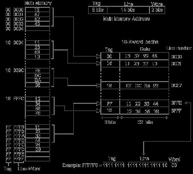
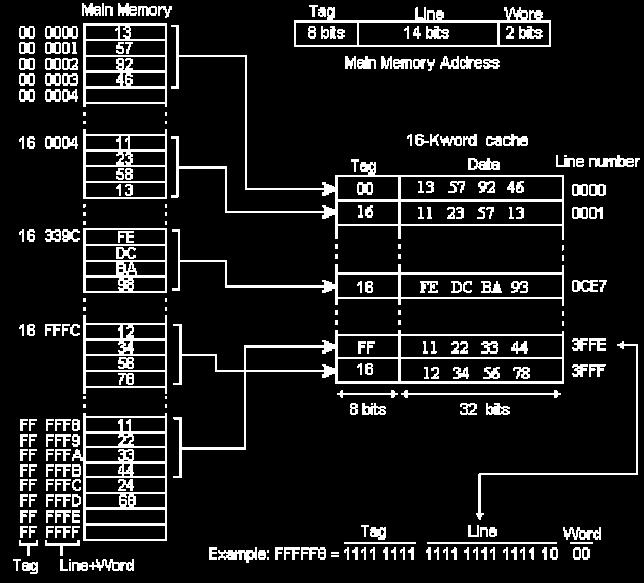
28 Tag (hex) Main memory address (binary) Tag Line + Word Data Tag Data Line Number FEDCBA98 16 FEDCBA98 0CE FF FFE 3FFF FF FF bits 32 bits 16-Kline cache FF FF bits 16-MByte main memory Note: Memory address values are in binary representation; other values are in hexadecimal Tag Line Word Main memory address = 8 bits 14 bits 2 bits Figure 4.10 Direct Mapping Example
29 + Direct Mapping Summary 29 Address length = (s + w) bits Number of addressable units = 2 s+w words or bytes Block size = line size = 2 w words or bytes Number of blocks in main memory = 2 s+ w /2 w = 2 s Number of lines in cache = m = 2 r Size of tag = (s r) bits
30 + Direct Mapping pros & cons 30 Simple Inexpensive Fixed location for given block If a program accesses 2 blocks that map to the same line repeatedly, cache misses are very high

31 + Victim Cache 31 Originally proposed as an approach to reduce the conflict misses of direct mapped caches without affecting its fast access time Fully associative cache Typical size is 4 to 16 cache lines Residing between direct mapped L1 cache and the next level of memory
32 s+w 32 Cache Main Memory s Memory Address Tag Word Tag Data L 0 W0 W1 W2 W3 B 0 w Compare 1 if match 0 if no match (hit in cache) s w L j L m 1 s w W4j W(4j+1) W(4j+2) W(4j+3) B j 0 if match 1 if no match (miss in cache) Figure 4.11 Fully Associative Cache Organization
33 Tag (hex) Main memory address (binary) Tag Word Data CE6 058CE7 058CE FEDCBA98 Tag 3FFFFE 058CE7 3FFFFD FFFFF Data FEDCBA98 FEDCBA Line Number FFD 3FFE 3FFF 22 bits 32 bits 16 Kline Cache 3FFFFD 3FFFFE 3FFFFF bits 16 MByte Main Memory Note: Memory address values are in binary representation; other values are in hexadecimal Main Memory Address = Tag Word 22 bits 2 bits Figure 4.12 Associative Mapping Example
34 + Associative Mapping Summary 34 Address length = (s + w) bits Number of addressable units = 2 s+w words or bytes Block size = line size = 2 w words or bytes Number of blocks in main memory = 2 s+ w /2 w = 2 s Number of lines in cache = undetermined Size of tag = s bits
35 + Set Associative Mapping 35 Compromise that exhibits the strengths of both the direct and associative approaches while reducing their disadvantages Cache consists of a number of sets Each set contains a number of lines A given block maps to any line in a given set e.g. 2 lines per set 2 way associative mapping A given block can be in one of 2 lines in only one set
36 v lines k lines B 0 L 0 36 B v 1 First v blocks of main memory (equal to number of sets) Cache memory - set 0 L k 1 Cache memory - set v 1 (a) v associative-mapped caches B 0 L 0 one set B v 1 First v blocks of main memory (equal to number of sets) Cache memory - way 1 Cache memory - way k L v 1 (b) k direct-mapped caches Figure 4.13 Mapping From Main Memory to Cache: k-way Set Associative
37 s+w 37 Cache Main Memory Tag Memory Address Set Word Tag Data F 0 B 0 s d d w F 1 B 1 Set 0 s d F k 1 F k s+w B j Compare F k+i Set 1 1 if match 0 if no match (hit in cache) F 2k 1 0 if match 1 if no match (miss in cache) Figure 4.14 k-way Set Associative Cache Organization
38 + Set Associative Mapping Summary 38 Address length = (s + w) bits Number of addressable units = 2 s+w words or bytes Block size = line size = 2 w words or bytes Number of blocks in main memory = 2 s+w/ 2 w= 2 s Number of lines in set = k Number of sets = v = 2 d Number of lines in cache = m=kv = k * 2 d Size of cache = k * 2 d+w words or bytes Size of tag = (s d) bits
39 Tag (hex) Main memory address (binary) Tag Set + Word Data Tag Main Memory Address = Set Word 39 9 bits 13 bits 2 bits C 02C Tag C Data Set Number Tag 02C Data C FEDCBA98 02C FEDCBA98 0CE7 02C FF 02C FFE 1FFF 1FF FF 1FF bits 32 bits 9 bits 16 Kline Cache 32 bits 1FF 1FF bits 16 MByte Main Memory Note: Memory address values are in binary representation; other values are in hexadecimal Figure 4.15 Two-Way Set Associative Mapping Example
40 Hit ratio k 2k 4k 8k 16k 32k 64k 128k 256k 512k 1M Cache size (bytes) direct 2-way 4-way 8-way 16-way Figure 4.16 Varying Associativity over Cache Size
41 + Replacement Algorithms 41 Once the cache has been filled, when a new block is brought into the cache, one of the existing blocks must be replaced For direct mapping there is only one possible line for any particular block and no choice is possible For the associative and set-associative techniques a replacement algorithm is needed To achieve high speed, an algorithm must be implemented in hardware
42 + The most common replacement 42 algorithms are: Least recently used (LRU) Most effective Replace that block in the set that has been in the cache longest with no reference to it Because of its simplicity of implementation, LRU is the most popular replacement algorithm First-in-first-out (FIFO) Replace that block in the set that has been in the cache longest Easily implemented as a round-robin or circular buffer technique Least frequently used (LFU) Replace that block in the set that has experienced the fewest references Could be implemented by associating a counter with each line


43 Write Policy 43 When a block that is resident in the cache is to be replaced there are two cases to consider: There are two problems to contend with: If the old block in the cache has not been altered then it may be overwritten with a new block without first writing out the old block More than one device may have access to main memory If at least one write operation has been performed on a word in that line of the cache then main memory must be updated by writing the line of cache out to the block of memory before bringing in the new block A more complex problem occurs when multiple processors are attached to the same bus and each processor has its own local cache - if a word is altered in one cache it could conceivably invalidate a word in other caches

44 + Write Through 44 and Write Back Write through Simplest technique All write operations are made to main memory as well as to the cache The main disadvantage of this technique is that it generates substantial memory traffic and may create a bottleneck Write back Minimizes memory writes Updates are made only in the cache Portions of main memory are invalid and hence accesses by I/O modules can be allowed only through the cache This makes for complex circuitry and a potential bottleneck


45 Line Size 45 When a block of data is retrieved and placed in the cache not only the desired word but also some number of adjacent words are retrieved As the block size increases more useful data are brought into the cache Two specific effects come into play: Larger blocks reduce the number of blocks that fit into a cache As a block becomes larger each additional word is farther from the requested word As the block size increases the hit ratio will at first increase because of the principle of locality The hit ratio will begin to decrease as the block becomes bigger and the probability of using the newly fetched information becomes less than the probability of reusing the information that has to be replaced
46 + Multilevel Caches 46 As logic density has increased it has become possible to have a cache on the same chip as the processor The on-chip cache reduces the processor s external bus activity and speeds up execution time and increases overall system performance When the requested instruction or data is found in the on-chip cache, the bus access is eliminated On-chip cache accesses will complete appreciably faster than would even zero-wait state bus cycles During this period the bus is free to support other transfers Two-level cache: Internal cache designated as level 1 (L1) External cache designated as level 2 (L2) Potential savings due to the use of an L2 cache depends on the hit rates in both the L1 and L2 caches The use of multilevel caches complicates all of the design issues related to caches, including size, replacement algorithm, and write policy
47 Hit ratio k 2k 4k 8k 16k 32k L1 = 16k L1 = 8k 64k 128k 256k 512k 1M 2M L2 Cache size (bytes) Figure 4.17 Total Hit Ratio (L1 and L2) for 8 Kbyte and 16 Kbyte L1
48 + Unified Versus Split Caches 48 Has become common to split cache: One dedicated to instructions One dedicated to data Both exist at the same level, typically as two L1 caches Advantages of unified cache: Higher hit rate Balances load of instruction and data fetches automatically Only one cache needs to be designed and implemented Trend is toward split caches at the L1 and unified caches for higher levels Advantages of split cache: Eliminates cache contention between instruction fetch/decode unit and execution unit Important in pipelining
49 Problem External memory slower than the system bus. Increased processor speed results in external bus becoming a bottleneck for cache access. Internal cache is rather small, due to limited space on chip Contention occurs when both the Instruction Prefetcher and the Execution Unit simultaneously require access to the cache. In that case, the Prefetcher is stalled while the Execution Unit s data access takes place. Increased processor speed results in external bus becoming a bottleneck for L2 cache access. Some applications deal with massive databases and must have rapid access to large amounts of data. The on-chip caches are too small. Solution Add external cache using faster memory technology. Move external cache onchip, operating at the same speed as the processor. Add external L2 cache using faster technology than main memory Create separate data and instruction caches. Create separate back-side bus that runs at higher speed than the main (front-side) external bus. The BSB is dedicated to the L2 cache. Move L2 cache on to the processor chip. Add external L3 cache. Processor on which Feature First Appears Pentium Pentium Pro Pentium II Pentium III Move L3 cache on-chip. Pentium 4 49 Table 4.4 Intel Cache Evolution (Table is on page 150 in the
50 50 System Bus Out-of-order execution logic L1 instruction cache (12K mops) Instruction fetch/decode unit 64 bits L3 cache (1 MB) Integer register file FP register file Load address unit Store address unit Simple integer ALU Simple integer ALU Complex integer ALU FP/ MMX unit FP move unit L2 cache (512 KB) L1 data cache (16 KB) 256 bits Figure 4.18 Pentium 4 Block Diagram
51 51 Table 4.5 Pentium 4 Cache Operating Modes Control Bits Operating Mode CD NW Cache Fills Write Throughs Invalidates 0 0 Enabled Enabled Enabled 1 0 Disabled Enabled Enabled 1 1 Disabled Disabled Disabled Note: CD = 0; NW = 1 is an invalid combination.
52 + Summary Chapter 4 Cache Memory 52 Computer memory system overview Characteristics of Memory Systems Memory Hierarchy Cache memory principles Pentium 4 cache organization Elements of cache design Cache addresses Cache size Mapping function Replacement algorithms Write policy Line size Number of caches
53 + A four-way set associative cache has lines of 8 bytes and a total size of 8kbytes. The 64Mbyte main memory is byte addressable. Show the format of main memory addresses. 53 Main Memory Size = 64Mbyte 2 26 Cache size = 8kbyte 2 13 Line has 8 bytes 4-way set associative cache = Set has 4 lines No. of Lines in Cache = 8kbyte / 8 = 1k Set = 1k/4= 256 TAG SET WORD
WEEK 7. Chapter 4. Cache Memory Pearson Education, Inc., Hoboken, NJ. All rights reserved.
 WEEK 7 + Chapter 4 Cache Memory Location Internal (e.g. processor registers, cache, main memory) External (e.g. optical disks, magnetic disks, tapes) Capacity Number of words Number of bytes Unit of Transfer
(Advanced) Computer Organization & Architechture. Prof. Dr. Hasan Hüseyin BALIK (4 th Week)
 Computer Organization & Architechture. Prof. Dr. Hasan Hüseyin BALIK (4 th Week)") + (Advanced) Computer Organization & Architechture Prof. Dr. Hasan Hüseyin BALIK (4 th Week) + Outline 2. The computer system 2.1 A Top-Level View of Computer Function and Interconnection 2.2 Cache Memory
+ (Advanced) Computer Organization & Architechture Prof. Dr. Hasan Hüseyin BALIK (4 th Week) + Outline 2. The computer system 2.1 A Top-Level View of Computer Function and Interconnection 2.2 Cache Memory
Memory Pearson Education, Inc., Hoboken, NJ. All rights reserved.
 1 Memory + 2 Location Internal (e.g. processor registers, cache, main memory) External (e.g. optical disks, magnetic disks, tapes) Capacity Number of words Number of bytes Unit of Transfer Word Block Access
Unit 2. Chapter 4 Cache Memory
 Unit 2 Chapter 4 Cache Memory Characteristics Location Capacity Unit of transfer Access method Performance Physical type Physical characteristics Organisation Location CPU Internal External Capacity Word
William Stallings Computer Organization and Architecture 8th Edition. Cache Memory
 William Stallings Computer Organization and Architecture 8th Edition Chapter 4 Cache Memory Characteristics Location Capacity Unit of transfer Access method Performance Physical type Physical characteristics
Eastern Mediterranean University School of Computing and Technology CACHE MEMORY. Computer memory is organized into a hierarchy.
 Eastern Mediterranean University School of Computing and Technology ITEC255 Computer Organization & Architecture CACHE MEMORY Introduction Computer memory is organized into a hierarchy. At the highest
TK2123: COMPUTER ORGANISATION & ARCHITECTURE. CPU and Memory (2)
") TK2123: COMPUTER ORGANISATION & ARCHITECTURE CPU and Memory (2) 1 Contents This lecture will discuss: Cache. Error Correcting Codes. 2 The Memory Hierarchy Trade-off: cost, capacity and access time. Faster
TK2123: COMPUTER ORGANISATION & ARCHITECTURE CPU and Memory (2) 1 Contents This lecture will discuss: Cache. Error Correcting Codes. 2 The Memory Hierarchy Trade-off: cost, capacity and access time. Faster
Chapter 4. Cache Memory. Yonsei University
 Chapter 4 Cache Memory Contents Computer Memory System Overview Cache Memory Principles Elements of Cache Design Pentium 4 and Power PC Cache 4-2 Key Characteristics 4-3 Location Processor Internal (main)
Chapter 4 Main Memory
 Chapter 4 Main Memory Course Outcome (CO) - CO2 Describe the architecture and organization of computer systems Program Outcome (PO) PO1 Apply knowledge of mathematics, science and engineering fundamentals
Overview IN this chapter we will study. William Stallings Computer Organization and Architecture 6th Edition
 William Stallings Computer Organization and Architecture 6th Edition Chapter 4 Cache Memory Overview IN this chapter we will study 4.1 COMPUTER MEMORY SYSTEM OVERVIEW 4.2 CACHE MEMORY PRINCIPLES 4.3 ELEMENTS
Computer & Microprocessor Architecture HCA103
 Computer & Microprocessor Architecture HCA103 Cache Memory UTM-RHH Slide Set 4 1 Characteristics Location Capacity Unit of transfer Access method Performance Physical type Physical characteristics Organisation
Characteristics of Memory Location wrt Motherboard. CSCI 4717 Computer Architecture. Characteristics of Memory Capacity Addressable Units
 CSCI 4717/5717 Computer Architecture Topic: Cache Memory Reading: Stallings, Chapter 4 Characteristics of Memory Location wrt Motherboard Inside CPU temporary memory or registers Motherboard main memory
Chapter 4 - Cache Memory
 Chapter 4 - Cache Memory Luis Tarrataca luis.tarrataca@gmail.com CEFET-RJ L. Tarrataca Chapter 4 - Cache Memory 1 / 143 Table of Contents I 1 Introduction 2 Computer Memory System Overview Characteristics
Characteristics. Microprocessor Design & Organisation HCA2102. Unit of Transfer. Location. Memory Hierarchy Diagram
 Microprocessor Design & Organisation HCA2102 Cache Memory Characteristics Location Unit of transfer Access method Performance Physical type Physical Characteristics UTM-RHH Slide Set 5 2 Location Internal
Cache memory. Lecture 4. Principles, structure, mapping
 Cache memory Lecture 4 Principles, structure, mapping Computer memory overview Computer memory overview By analyzing memory hierarchy from top to bottom, the following conclusions can be done: a. Cost
Memory Hierarchy Recall the von Neumann bottleneck - single, relatively slow path between the CPU and main memory.
 Memory Hierarchy Goal: Fast, unlimited storage at a reasonable cost per bit. Recall the von Neumann bottleneck - single, relatively slow path between the CPU and main memory. Cache - 1 Typical system view
Chapter 1 Computer System Overview
 Operating Systems: Internals and Design Principles Chapter 1 Computer System Overview Ninth Edition By William Stallings Operating System Exploits the hardware resources of one or more processors Provides
CSC 553 Operating Systems
 CSC 553 Operating Systems Lecture 1- Computer System Overview Operating System Exploits the hardware resources of one or more processors Provides a set of services to system users Manages secondary memory
Contents. Memory System Overview Cache Memory. Internal Memory. Virtual Memory. Memory Hierarchy. Registers In CPU Internal or Main memory
 Memory Hierarchy Contents Memory System Overview Cache Memory Internal Memory External Memory Virtual Memory Memory Hierarchy Registers In CPU Internal or Main memory Cache RAM External memory Backing
COMPUTER ARCHITECTURE AND ORGANIZATION
 Memory System 1. Microcomputer Memory Memory is an essential component of the microcomputer system. It stores binary instructions and datum for the microcomputer. The memory is the place where the computer
The Memory System. Components of the Memory System. Problems with the Memory System. A Solution
 Datorarkitektur Fö 2-1 Datorarkitektur Fö 2-2 Components of the Memory System The Memory System 1. Components of the Memory System Main : fast, random access, expensive, located close (but not inside)
Physical characteristics (such as packaging, volatility, and erasability Organization.
 CS 320 Ch 4 Cache Memory 1. The author list 8 classifications for memory systems; Location Capacity Unit of transfer Access method (there are four:sequential, Direct, Random, and Associative) Performance
Computer Organization. Chapter 12: Memory organization
 Computer Organization Chapter 12: Memory organization Memory Organization Recall: Information is stored in the memory as a collection of bits. Collection of bits that are stored or retrieved simultaneously
Lecture 2: Memory Systems
 Lecture 2: Memory Systems Basic components Memory hierarchy Cache memory Virtual Memory Zebo Peng, IDA, LiTH Many Different Technologies Zebo Peng, IDA, LiTH 2 Internal and External Memories CPU Date transfer
UNIT-V MEMORY ORGANIZATION
 UNIT-V MEMORY ORGANIZATION 1 The main memory of a computer is semiconductor memory.the main memory unit is basically consists of two kinds of memory: RAM (RWM):Random access memory; which is volatile in
CPU issues address (and data for write) Memory returns data (or acknowledgment for write)
 Memory returns data (or acknowledgment for write)") The Main Memory Unit CPU and memory unit interface Address Data Control CPU Memory CPU issues address (and data for write) Memory returns data (or acknowledgment for write) Memories: Design Objectives
The Main Memory Unit CPU and memory unit interface Address Data Control CPU Memory CPU issues address (and data for write) Memory returns data (or acknowledgment for write) Memories: Design Objectives
Advanced Memory Organizations
 CSE 3421: Introduction to Computer Architecture Advanced Memory Organizations Study: 5.1, 5.2, 5.3, 5.4 (only parts) Gojko Babić 03-29-2018 1 Growth in Performance of DRAM & CPU Huge mismatch between CPU
Chapter 1 Computer System Overview
 Operating Systems: Internals and Design Principles Chapter 1 Computer System Overview Ninth Edition By William Stallings Operating System Exploits the hardware resources of one or more processors Provides
CHAPTER 6 Memory. CMPS375 Class Notes (Chap06) Page 1 / 20 Dr. Kuo-pao Yang
 Page 1 / 20 Dr. Kuo-pao Yang") CHAPTER 6 Memory 6.1 Memory 341 6.2 Types of Memory 341 6.3 The Memory Hierarchy 343 6.3.1 Locality of Reference 346 6.4 Cache Memory 347 6.4.1 Cache Mapping Schemes 349 6.4.2 Replacement Policies 365
CHAPTER 6 Memory 6.1 Memory 341 6.2 Types of Memory 341 6.3 The Memory Hierarchy 343 6.3.1 Locality of Reference 346 6.4 Cache Memory 347 6.4.1 Cache Mapping Schemes 349 6.4.2 Replacement Policies 365
CPE300: Digital System Architecture and Design
 CPE300: Digital System Architecture and Design Fall 2011 MW 17:30-18:45 CBC C316 Virtual Memory 11282011 http://www.egr.unlv.edu/~b1morris/cpe300/ 2 Outline Review Cache Virtual Memory Projects 3 Memory
Cache Memory Part 1. Cache Memory Part 1 1
 Cache Memory Part 1 Cache Memory Part 1 1 - Definition: Cache (Pronounced as cash ) is a small and very fast temporary storage memory. It is designed to speed up the transfer of data and instructions.
Computer Organization (Autonomous)
") 2-7-27 Computer Organization (Autonomous) UNIT IV Sections - A & D SYLLABUS The Memory System: Memory Hierarchy, - RAM and ROM Chips, Memory Address Maps, Memory Connection to, Auxiliary Magnetic Disks,
2-7-27 Computer Organization (Autonomous) UNIT IV Sections - A & D SYLLABUS The Memory System: Memory Hierarchy, - RAM and ROM Chips, Memory Address Maps, Memory Connection to, Auxiliary Magnetic Disks,
Q.1 Explain Computer s Basic Elements
 Q.1 Explain Computer s Basic Elements Ans. At a top level, a computer consists of processor, memory, and I/O components, with one or more modules of each type. These components are interconnected in some
LECTURE 11. Memory Hierarchy
 LECTURE 11 Memory Hierarchy MEMORY HIERARCHY When it comes to memory, there are two universally desirable properties: Large Size: ideally, we want to never have to worry about running out of memory. Speed
MEMORY. Objectives. L10 Memory
 MEMORY Reading: Chapter 6, except cache implementation details (6.4.1-6.4.6) and segmentation (6.5.5) https://en.wikipedia.org/wiki/probability 2 Objectives Understand the concepts and terminology of hierarchical
Chapter 6 Memory 11/3/2015. Chapter 6 Objectives. 6.2 Types of Memory. 6.1 Introduction
 Chapter 6 Objectives Chapter 6 Memory Master the concepts of hierarchical memory organization. Understand how each level of memory contributes to system performance, and how the performance is measured.
Memory. Objectives. Introduction. 6.2 Types of Memory
 Memory Objectives Master the concepts of hierarchical memory organization. Understand how each level of memory contributes to system performance, and how the performance is measured. Master the concepts
CS 152 Computer Architecture and Engineering. Lecture 7 - Memory Hierarchy-II
 CS 152 Computer Architecture and Engineering Lecture 7 - Memory Hierarchy-II Krste Asanovic Electrical Engineering and Computer Sciences University of California at Berkeley http://www.eecs.berkeley.edu/~krste!
The Memory Hierarchy & Cache
 Removing The Ideal Memory Assumption: The Memory Hierarchy & Cache The impact of real memory on CPU Performance. Main memory basic properties: Memory Types: DRAM vs. SRAM The Motivation for The Memory
GUJARAT TECHNOLOGICAL UNIVERSITY MASTER OF COMPUTER APPLICATION SEMESTER: III
 GUJARAT TECHNOLOGICAL UNIVERSITY MASTER OF COMPUTER APPLICATION SEMESTER: III Subject Name: Operating System (OS) Subject Code: 630004 Unit-1: Computer System Overview, Operating System Overview, Processes
Cache Memory COE 403. Computer Architecture Prof. Muhamed Mudawar. Computer Engineering Department King Fahd University of Petroleum and Minerals
 Cache Memory COE 403 Computer Architecture Prof. Muhamed Mudawar Computer Engineering Department King Fahd University of Petroleum and Minerals Presentation Outline The Need for Cache Memory The Basics
LECTURE 10: Improving Memory Access: Direct and Spatial caches
 EECS 318 CAD Computer Aided Design LECTURE 10: Improving Memory Access: Direct and Spatial caches Instructor: Francis G. Wolff wolff@eecs.cwru.edu Case Western Reserve University This presentation uses
Chapter Seven. Memories: Review. Exploiting Memory Hierarchy CACHE MEMORY AND VIRTUAL MEMORY
 Chapter Seven CACHE MEMORY AND VIRTUAL MEMORY 1 Memories: Review SRAM: value is stored on a pair of inverting gates very fast but takes up more space than DRAM (4 to 6 transistors) DRAM: value is stored
and data combined) is equal to 7% of the number of instructions. Miss Rate with Second- Level Cache, Direct- Mapped Speed
 is equal to 7% of the number of instructions. Miss Rate with Second- Level Cache, Direct- Mapped Speed") 5.3 By convention, a cache is named according to the amount of data it contains (i.e., a 4 KiB cache can hold 4 KiB of data); however, caches also require SRAM to store metadata such as tags and valid
5.3 By convention, a cache is named according to the amount of data it contains (i.e., a 4 KiB cache can hold 4 KiB of data); however, caches also require SRAM to store metadata such as tags and valid
EE 4683/5683: COMPUTER ARCHITECTURE
 EE 4683/5683: COMPUTER ARCHITECTURE Lecture 6A: Cache Design Avinash Kodi, kodi@ohioedu Agenda 2 Review: Memory Hierarchy Review: Cache Organization Direct-mapped Set- Associative Fully-Associative 1 Major
CHAPTER 6 Memory. CMPS375 Class Notes Page 1/ 16 by Kuo-pao Yang
 CHAPTER 6 Memory 6.1 Memory 233 6.2 Types of Memory 233 6.3 The Memory Hierarchy 235 6.3.1 Locality of Reference 237 6.4 Cache Memory 237 6.4.1 Cache Mapping Schemes 239 6.4.2 Replacement Policies 247
Memory hierarchy and cache
 Memory hierarchy and cache QUIZ EASY 1). What is used to design Cache? a). SRAM b). DRAM c). Blend of both d). None. 2). What is the Hierarchy of memory? a). Processor, Registers, Cache, Tape, Main memory,
EE414 Embedded Systems Ch 5. Memory Part 2/2
 EE414 Embedded Systems Ch 5. Memory Part 2/2 Byung Kook Kim School of Electrical Engineering Korea Advanced Institute of Science and Technology Overview 6.1 introduction 6.2 Memory Write Ability and Storage
CS3350B Computer Architecture
 CS335B Computer Architecture Winter 25 Lecture 32: Exploiting Memory Hierarchy: How? Marc Moreno Maza wwwcsduwoca/courses/cs335b [Adapted from lectures on Computer Organization and Design, Patterson &
Computer Organization and Assembly Language (CS-506)
") Computer Organization and Assembly Language (CS-506) Muhammad Zeeshan Haider Ali Lecturer ISP. Multan ali.zeeshan04@gmail.com https://zeeshanaliatisp.wordpress.com/ Lecture 2 Memory Organization and Structure
Computer Organization and Assembly Language (CS-506) Muhammad Zeeshan Haider Ali Lecturer ISP. Multan ali.zeeshan04@gmail.com https://zeeshanaliatisp.wordpress.com/ Lecture 2 Memory Organization and Structure
Chapter 5A. Large and Fast: Exploiting Memory Hierarchy
 Chapter 5A Large and Fast: Exploiting Memory Hierarchy Memory Technology Static RAM (SRAM) Fast, expensive Dynamic RAM (DRAM) In between Magnetic disk Slow, inexpensive Ideal memory Access time of SRAM
Overview. EE 4504 Computer Organization. Historically, the limiting factor in a computer s performance has been memory access time
 Overview EE 4504 Computer Organization Section 3 Computer Memory Historically, the limiting factor in a computer s performance has been memory access time Memory speed has been slow compared to the speed
A Review on Cache Memory with Multiprocessor System
 A Review on Cache Memory with Multiprocessor System Chirag R. Patel 1, Rajesh H. Davda 2 1,2 Computer Engineering Department, C. U. Shah College of Engineering & Technology, Wadhwan (Gujarat) Abstract
The Central Processing Unit
 The Central Processing Unit All computers derive from the same basic design, usually referred to as the von Neumann architecture. This concept involves solving a problem by defining a sequence of commands
Contents. Main Memory Memory access time Memory cycle time. Types of Memory Unit RAM ROM
 Memory Organization Contents Main Memory Memory access time Memory cycle time Types of Memory Unit RAM ROM Memory System Virtual Memory Cache Memory - Associative mapping Direct mapping Set-associative
Page 1. Multilevel Memories (Improving performance using a little cash )
") Page 1 Multilevel Memories (Improving performance using a little cash ) 1 Page 2 CPU-Memory Bottleneck CPU Memory Performance of high-speed computers is usually limited by memory bandwidth & latency Latency
Page 1 Multilevel Memories (Improving performance using a little cash ) 1 Page 2 CPU-Memory Bottleneck CPU Memory Performance of high-speed computers is usually limited by memory bandwidth & latency Latency
CS 152 Computer Architecture and Engineering. Lecture 7 - Memory Hierarchy-II
 CS 152 Computer Architecture and Engineering Lecture 7 - Memory Hierarchy-II Krste Asanovic Electrical Engineering and Computer Sciences University of California at Berkeley http://www.eecs.berkeley.edu/~krste
EITF20: Computer Architecture Part 5.1.1: Virtual Memory
 EITF20: Computer Architecture Part 5.1.1: Virtual Memory Liang Liu liang.liu@eit.lth.se 1 Outline Reiteration Cache optimization Virtual memory Case study AMD Opteron Summary 2 Memory hierarchy 3 Cache
Chapter 8. Virtual Memory
 Operating System Chapter 8. Virtual Memory Lynn Choi School of Electrical Engineering Motivated by Memory Hierarchy Principles of Locality Speed vs. size vs. cost tradeoff Locality principle Spatial Locality:
Operating system Dr. Shroouq J.
 2.2.2 DMA Structure In a simple terminal-input driver, when a line is to be read from the terminal, the first character typed is sent to the computer. When that character is received, the asynchronous-communication
Chapter 6 Objectives
 Chapter 6 Memory Chapter 6 Objectives Master the concepts of hierarchical memory organization. Understand how each level of memory contributes to system performance, and how the performance is measured.
B.H.GARDI COLLEGE OF MASTER OF COMPUTER APPLICATION
 Introduction :- An exploits the hardware resources of one or more processors to provide a set of services to system users. The OS also manages secondary memory and I/O devices on behalf of its users. So
Memory Organization MEMORY ORGANIZATION. Memory Hierarchy. Main Memory. Auxiliary Memory. Associative Memory. Cache Memory.
 MEMORY ORGANIZATION Memory Hierarchy Main Memory Auxiliary Memory Associative Memory Cache Memory Virtual Memory MEMORY HIERARCHY Memory Hierarchy Memory Hierarchy is to obtain the highest possible access
Page 1. Memory Hierarchies (Part 2)
") Memory Hierarchies (Part ) Outline of Lectures on Memory Systems Memory Hierarchies Cache Memory 3 Virtual Memory 4 The future Increasing distance from the processor in access time Review: The Memory Hierarchy
Memory Hierarchies (Part ) Outline of Lectures on Memory Systems Memory Hierarchies Cache Memory 3 Virtual Memory 4 The future Increasing distance from the processor in access time Review: The Memory Hierarchy
A Cache Hierarchy in a Computer System
 A Cache Hierarchy in a Computer System Ideally one would desire an indefinitely large memory capacity such that any particular... word would be immediately available... We are... forced to recognize the
www-inst.eecs.berkeley.edu/~cs61c/
 CS61C Machine Structures Lecture 34 - Caches II 11/16/2007 John Wawrzynek (www.cs.berkeley.edu/~johnw) www-inst.eecs.berkeley.edu/~cs61c/ 1 What to do on a write hit? Two Options: Write-through update
Performance metrics for caches
 Performance metrics for caches Basic performance metric: hit ratio h h = Number of memory references that hit in the cache / total number of memory references Typically h = 0.90 to 0.97 Equivalent metric:
William Stallings Computer Organization and Architecture 8th Edition. Chapter 5 Internal Memory
 William Stallings Computer Organization and Architecture 8th Edition Chapter 5 Internal Memory Semiconductor Memory The basic element of a semiconductor memory is the memory cell. Although a variety of
CS161 Design and Architecture of Computer Systems. Cache $$$$$
 CS161 Design and Architecture of Computer Systems Cache $$$$$ Memory Systems! How can we supply the CPU with enough data to keep it busy?! We will focus on memory issues,! which are frequently bottlenecks
Fig 7.30 The Cache Mapping Function. Memory Fields and Address Translation
 7-47 Chapter 7 Memory System Design Fig 7. The Mapping Function Example: KB MB CPU Word Block Main Address Mapping function The cache mapping function is responsible for all cache operations: Placement
Computer System Overview OPERATING SYSTEM TOP-LEVEL COMPONENTS. Simplified view: Operating Systems. Slide 1. Slide /S2. Slide 2.
 BASIC ELEMENTS Simplified view: Processor Slide 1 Computer System Overview Operating Systems Slide 3 Main Memory referred to as real memory or primary memory volatile modules 2004/S2 secondary memory devices
CSF Improving Cache Performance. [Adapted from Computer Organization and Design, Patterson & Hennessy, 2005]
![CSF Improving Cache Performance. [Adapted from Computer Organization and Design, Patterson & Hennessy, 2005]](/thumbs/76/74076691.jpg "CSF Improving Cache Performance. [Adapted from Computer Organization and Design, Patterson & Hennessy, 2005]") CSF Improving Cache Performance [Adapted from Computer Organization and Design, Patterson & Hennessy, 2005] Review: The Memory Hierarchy Take advantage of the principle of locality to present the user
CSF Improving Cache Performance [Adapted from Computer Organization and Design, Patterson & Hennessy, 2005] Review: The Memory Hierarchy Take advantage of the principle of locality to present the user
Course Administration
 Spring 207 EE 363: Computer Organization Chapter 5: Large and Fast: Exploiting Memory Hierarchy - Avinash Kodi Department of Electrical Engineering & Computer Science Ohio University, Athens, Ohio 4570
Chapter 5 Memory Hierarchy Design. In-Cheol Park Dept. of EE, KAIST
 Chapter 5 Memory Hierarchy Design In-Cheol Park Dept. of EE, KAIST Why cache? Microprocessor performance increment: 55% per year Memory performance increment: 7% per year Principles of locality Spatial
MIPS) ( MUX
 ( MUX") Memory What do we use for accessing small amounts of data quickly? Registers (32 in MIPS) Why not store all data and instructions in registers? Too much overhead for addressing; lose speed advantage Register
Memory What do we use for accessing small amounts of data quickly? Registers (32 in MIPS) Why not store all data and instructions in registers? Too much overhead for addressing; lose speed advantage Register
Computer Organization
 University of Pune S.E. I.T. Subject code: 214442 Computer Organization Part 20 : Memory Organization Basics UNIT IV Tushar B. Kute, Department of Information Technology, Sandip Institute of Technology
MICROPROCESSOR MEMORY ORGANIZATION
 MICROPROCESSOR MEMORY ORGANIZATION 1 3.1 Introduction 3.2 Main memory 3.3 Microprocessor on-chip memory management unit and cache 2 A memory unit is an integral part of any microcomputer, and its primary
k -bit address bus n-bit data bus Control lines ( R W, MFC, etc.)
") THE MEMORY SYSTEM SOME BASIC CONCEPTS Maximum size of the Main Memory byte-addressable CPU-Main Memory Connection, Processor MAR MDR k -bit address bus n-bit data bus Memory Up to 2 k addressable locations
THE MEMORY SYSTEM SOME BASIC CONCEPTS Maximum size of the Main Memory byte-addressable CPU-Main Memory Connection, Processor MAR MDR k -bit address bus n-bit data bus Memory Up to 2 k addressable locations
Memory memories memory
 Memory Organization Memory Hierarchy Memory is used for storing programs and data that are required to perform a specific task. For CPU to operate at its maximum speed, it required an uninterrupted and
Caches Concepts Review
 Caches Concepts Review What is a block address? Why not bring just what is needed by the processor? What is a set associative cache? Write-through? Write-back? Then we ll see: Block allocation policy on
Advanced Parallel Architecture Lesson 4. Annalisa Massini /2015
 Advanced Parallel Architecture Lesson 4 Annalisa Massini - Modules and connections 2 Components and connections The CU and the ALU constitute the Central Processing Unit Data and instructions need to get
High Performance Computer Architecture Prof. Ajit Pal Department of Computer Science and Engineering Indian Institute of Technology, Kharagpur
 High Performance Computer Architecture Prof. Ajit Pal Department of Computer Science and Engineering Indian Institute of Technology, Kharagpur Lecture - 23 Hierarchical Memory Organization (Contd.) Hello
Improving Cache Performance and Memory Management: From Absolute Addresses to Demand Paging. Highly-Associative Caches
 Improving Cache Performance and Memory Management: From Absolute Addresses to Demand Paging 6.823, L8--1 Asanovic Laboratory for Computer Science M.I.T. http://www.csg.lcs.mit.edu/6.823 Highly-Associative
Cache Performance and Memory Management: From Absolute Addresses to Demand Paging. Cache Performance
 6.823, L11--1 Cache Performance and Memory Management: From Absolute Addresses to Demand Paging Asanovic Laboratory for Computer Science M.I.T. http://www.csg.lcs.mit.edu/6.823 Cache Performance 6.823,
Lecture 16. Today: Start looking into memory hierarchy Cache$! Yay!
 Lecture 16 Today: Start looking into memory hierarchy Cache$! Yay! Note: There are no slides labeled Lecture 15. Nothing omitted, just that the numbering got out of sequence somewhere along the way. 1
Microprocessors I MICROCOMPUTERS AND MICROPROCESSORS
 Microprocessors I Outline of the Lecture Microcomputers and Microprocessors Evolution of Intel 80x86 Family Microprocessors Binary and Hexadecimal Number Systems MICROCOMPUTERS AND MICROPROCESSORS There
Memory Hierarchy. Goal: Fast, unlimited storage at a reasonable cost per bit.
 Memory Hierarchy Goal: Fast, unlimited storage at a reasonable cost per bit. Recall the von Neumann bottleneck - single, relatively slow path between the CPU and main memory. Fast: When you need something
Module 5a: Introduction To Memory System (MAIN MEMORY)
") Module 5a: Introduction To Memory System (MAIN MEMORY) R E F E R E N C E S : S T A L L I N G S, C O M P U T E R O R G A N I Z A T I O N A N D A R C H I T E C T U R E M O R R I S M A N O, C O M P U T E
Module 5a: Introduction To Memory System (MAIN MEMORY) R E F E R E N C E S : S T A L L I N G S, C O M P U T E R O R G A N I Z A T I O N A N D A R C H I T E C T U R E M O R R I S M A N O, C O M P U T E
EECS151/251A Spring 2018 Digital Design and Integrated Circuits. Instructors: John Wawrzynek and Nick Weaver. Lecture 19: Caches EE141
 EECS151/251A Spring 2018 Digital Design and Integrated Circuits Instructors: John Wawrzynek and Nick Weaver Lecture 19: Caches Cache Introduction 40% of this ARM CPU is devoted to SRAM cache. But the role
UNIT:4 MEMORY ORGANIZATION
 1 UNIT:4 MEMORY ORGANIZATION TOPICS TO BE COVERED. 4.1 Memory Hierarchy 4.2 Memory Classification 4.3 RAM,ROM,PROM,EPROM 4.4 Main Memory 4.5Auxiliary Memory 4.6 Associative Memory 4.7 Cache Memory 4.8
Concept of Memory. The memory of computer is broadly categories into two categories:
 Concept of Memory We have already mentioned that digital computer works on stored programmed concept introduced by Von Neumann. We use memory to store the information, which includes both program and data.
Computer System Overview
 Computer System Overview Operating Systems 2005/S2 1 What are the objectives of an Operating System? 2 What are the objectives of an Operating System? convenience & abstraction the OS should facilitate
Memory Design. Cache Memory. Processor operates much faster than the main memory can.
 Memory Design Cache Memory Processor operates much faster than the main memory can. To ameliorate the sitution, a high speed memory called a cache memory placed between the processor and main memory. Barry
Memory Hierarchy Y. K. Malaiya
 Memory Hierarchy Y. K. Malaiya Acknowledgements Computer Architecture, Quantitative Approach - Hennessy, Patterson Vishwani D. Agrawal Review: Major Components of a Computer Processor Control Datapath
Computer Organization
 University of Pune S.E. I.T. Subject code: 214442 Computer Organization Part 20 : Memory Organization Basics UNIT IV Tushar B. Kute, Department of Information Technology, Sandip Institute of Technology
The levels of a memory hierarchy. Main. Memory. 500 By 1MB 4GB 500GB 0.25 ns 1ns 20ns 5ms
 The levels of a memory hierarchy CPU registers C A C H E Memory bus Main Memory I/O bus External memory 500 By 1MB 4GB 500GB 0.25 ns 1ns 20ns 5ms 1 1 Some useful definitions When the CPU finds a requested
Plot SIZE. How will execution time grow with SIZE? Actual Data. int array[size]; int A = 0;
![Plot SIZE. How will execution time grow with SIZE? Actual Data. int array[size]; int A = 0;](/thumbs/75/72768059.jpg "Plot SIZE. How will execution time grow with SIZE? Actual Data. int array[size]; int A = 0;") How will execution time grow with SIZE? int array[size]; int A = ; for (int i = ; i < ; i++) { for (int j = ; j < SIZE ; j++) { A += array[j]; } TIME } Plot SIZE Actual Data 45 4 5 5 Series 5 5 4 6 8 Memory
How will execution time grow with SIZE? int array[size]; int A = ; for (int i = ; i < ; i++) { for (int j = ; j < SIZE ; j++) { A += array[j]; } TIME } Plot SIZE Actual Data 45 4 5 5 Series 5 5 4 6 8 Memory
ECE Lab 8. Logic Design for a Direct-Mapped Cache. To understand the function and design of a direct-mapped memory cache.
 ECE 201 - Lab 8 Logic Design for a Direct-Mapped Cache PURPOSE To understand the function and design of a direct-mapped memory cache. EQUIPMENT Simulation Software REQUIREMENTS Electronic copy of your
CS356: Discussion #9 Memory Hierarchy and Caches. Marco Paolieri Illustrations from CS:APP3e textbook
 CS356: Discussion #9 Memory Hierarchy and Caches Marco Paolieri (paolieri@usc.edu) Illustrations from CS:APP3e textbook The Memory Hierarchy So far... We modeled the memory system as an abstract array
CPE300: Digital System Architecture and Design
 CPE300: Digital System Architecture and Design Fall 2011 MW 17:30-18:45 CBC C316 Cache 11232011 http://www.egr.unlv.edu/~b1morris/cpe300/ 2 Outline Review Memory Components/Boards Two-Level Memory Hierarchy