3D SYSTEM INTEGRATION TECHNOLOGY CHOICES AND CHALLENGE ERIC BEYNE, ANTONIO LA MANNA
|
|
|
- Olivia Stanley
- 6 years ago
- Views:
Transcription


1 3D SYSTEM INTEGRATION TECHNOLOGY CHOICES AND CHALLENGE ERIC BEYNE, ANTONIO LA MANNA

2 OUTLINE 3D Application Drivers and Roadmap 3D Stacked-IC Technology 3D System-on-Chip: Fine grain partitioning Conclusion 3D Landscape 2


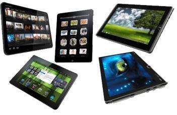

3 APPLICATION DRIVERS Facebook 3
4 APPLICATION DRIVERS More Data; Faster Data Increased Power Consumption 4

5 APPLICATION DRIVERS More Data; Faster Data 3D Stacked IC s 3D-SIC Interposer stacking 5
6 MAIN APPLICATIONS DRIVERS 3D INTEGRATION TECHNOLOGY DRAM DRAM Logic Logic Memory cube Offers low delay, low power and high bandwidth interconnect. High volume applications: drives the technology platforms 6
7 MAIN APPLICATIONS DRIVERS 3D INTEGRATION TECHNOLOGY DRAM DRAM Logic Logic Close to market introduction but delayed with respect to original timelines: osupply chain readiness: wide I/O memory supply, unclear business models otechnology readiness and cost of ownership, CoO. Memory cube ohigh performance applications: high power: requires the use of an intermediate interposer technology = additional cost: needs to be offset by additional integration opportunities. 7
8 High Power Low Volume High performance Low Power High Volume Consumer 3D APPLICATION ROADMAP Memory cube DRAM on Logic Heterogeneous Mixed Analog/Digital DRAM on Logic Logic/DRAM on CSP Si interposer Mixed node 3D-SOC Analog/ MEMS/Sensors Digital Logic Analog E/O Logic fabric N+1 N/N-1 Heterogeneous smart system integration Optical Module DRAM Logic DRAM Logic/ ASPs/Analog/IO DRAM Logic OIO Passive interposer Processing unit with high bandwidth electrical I/O integrated on lite - active Silicon Interposer Processing unit with optical I/O integrated on lite -active Silicon Interposer 8
9 OUTLINE 3D Application Drivers and Roadmap 3D Stacked-IC Technology 3D System-on-Chip: Fine grain partitioning Conclusion 3D Landscape 9
 or lateral")
 Technologies are available for successful")

10 3DSIC: STACKED IC INTEGRATION High density die-die interconnect: vertical (3D) or lateral interconnect on interposer substrate ( 2.5D ) Technologies are available for successful integration Key challenges: Cost effective integration schemes Technology maturity Business models 10


")
11 3D TECHNOLOGY: FROM TSV TO STACKED PACKAGE FEOL process Via middle TSV BEOL process Wafer thinning, TSV reveal & backside processing Via last TSV 3D Stacking (D2D; D2W; W2W) Stack Packaging 11

12 3D TECHNOLOGY: MAIN CHALLENGES FROM TSV TO STACKED PACKAGE FEOL process Via middle TSV BEOL process Wafer thinning, TSV reveal & backside processing Via last TSV Via Middle TSV POR process at 5µm Ø x 50 µm Si thickness Reliable process at 3µm Ø x 50 µm Si thickness Potential scaling to 2µm Ø x 40 µm Si thickness Cost effective, reliable temporary thin wafer carrier system. Proposed solutions and materials still evolving Via Last TSV: low thermal budget, Si TTV, M1 contact Scaling to 5µm Ø x 50 µm Si thickness 3D Stacking (D2D; D2W; W2W) Stack Packaging Die level: Interconnect pitch scaling, assembly yield and productivity (throughput). Wafer level: Wafer-to-wafer overlay, Bonding yield Electrical interconnect method and yield. CPI : 3D stack or interposer to package stacking Thermal control 12


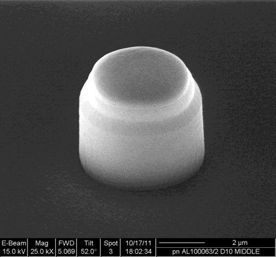
13 VIA MIDDLE Cu TSV PROCESS AFTER FEOL / BEFORE BEOL Si Si imec POR process: o 5 µm diameter; o 50 µm deep; o Aspect ratio 10 13


14 3D- TSV SCALING ROADMAP 10µm Ø, 100µm deep, AR 10:1 5µm Ø, 50µm deep AR 10:1 3µm Ø, 50µm deep AR 17:1 2µm Ø, 40µm deep AR 15:1 20:1 Ø AR Depth Ø AR Depth 30µm 40µm In combination with integration on advanced device nodes 14


15 DIE-TO-DIE OR DIE-TO-WAFER STACKING - Scaling to 20µm µbump PITCH 12.5µm 7.5µm Cu Sn Ni 20µm Cu Sn Cu pad Cu pad 12.5µm 7.5µm 15


16 DIRECT CU TSV-TO-CU PAD STACKING 6 die stack (20 µm pitch) - TSV Cu TSV liner 5µm Backside Passivation 20µm 16
17 OUTLINE 3D Application Drivers and Roadmap 3D Stacked-IC Technology 3D System-on-Chip: Fine grain partitioning Conclusion 3D Landscape 17


18 HIGH DENSITY 3D-INTEGRATION 3D-SOC : 3D System-on-chip, through heterogeneous integration SOC Node N Node N+1 Digital logic takes full advantage of scaling Efficient use wafer area Node N/N+1 Digital Logic, SRAM Analog functionality I/O drivers High density SRAM on logic Mixed node, heterogeneous technology Wafer-Wafer bonding High density Wafer-wafer interconnects: Pitch scaling 5µm 2 µm 1 µm 0.5µm 18


19 3D ARCHITECTURE EXPLORATION EXAMPLE IMEC S SOC 3MF AVC/H264 ENCODER L2I1 L2D1 L2I2 L2D2 L2I1 L2D1 AD#1 AD#2 AD#3 L2D2 AD#6 AD#5 AD#4 L2I2 AD#1 AD#2 AD#1 AD#1 AD#2 AD#3 AD#2 L1#1 AD#3 AD#3 L1#2 L1#3 L1#6 AD#6 AD#5 L1#5 AD#6 AD#6 AD#4 L1#4 AD#5 AD#5 AD#4 AD#4 3D-SIC 3D SOC / CONFIDENTIAL 19

20 BEOL ELECTRONIC SYSTEM INTERCONNECT WIRING HIERARCHY On-chip Wiring Hierarchy System-level wiring hierarchy Traditional view Global Inter - mediate Local FEOL ITRS 20
21 3D SOC W2W BONDING Both wafers have FEOL and BEOL processing Top wafer has FEOL and some BEOL processing Bottom wafer has FEOL and BEOL processing Contact pitch 5µm 1µm Minimal processing after bonding: via reveal or via last Contact pitch 2µm 0.5µm Critical processing after bonding: High AR small TSV - via to top and bottom wafer metalization One or more BEOL layers after wafer stacking 21


22 3D-SOC - W2W HYBRID BONDING TSV Oxide-oxide bonding Cu Cu connection 22
23 2 ND TIER FEOL PROCESSING POST WAFER BONDING Top wafer: only unpattern semiconductor device layer Bottom wafer has FEOL and some BEOL processing Simplified bonding process: no overlay problem Critical processing after bonding: Device fabrication second tier with very low thermal budget (with Cu/low-k BEOL tier 1 present) When connecting at fine pitch: Most of the BEOL layers to be processed after wafer stacking 23
24 OUTLINE 3D Application Drivers and Roadmap 3D Stacked-IC Technology 3D System-on-Chip: Fine grain partitioning Conclusion 3D Landscape 24
25 3D LANDSCAPE 3D-SIC 3D-SOC 3D-IC wiring level Global Semi-global Intermediate Local FEOL 2-tier stack 2 nd FEOL after stacking Multi-tier FEOL TSV Pitch µm µm TSV after stack TSV after stack No TSV Contact Pitch: Rel. density: Stacking Method µbump pitch: µm Cu TSV Cu pad: µm D2D, D2W (W2W) Stacked die B2F / F2F 5 1 µm µm 0.5 µm (Overlay 2 nd tier defined by W2W alignment/bonding) W2W (D2W) Contact at bond interface F2F W2W Contact after stacking F2F nm W2W Si layer-to-wafer stacking 2 nd Tier Device fab. after stacking < 100 nm > (Overlay 2 nd tier defined by litho scanner alignment) Monolithic Device-level stacking 25
26 3D LANDSCAPE 3D-SIC 3D-SOC 3D-IC wiring level Global Semi-global Intermediate Local FEOL 2-tier stack 2 nd FEOL after stacking Multi-tier FEOL TSV Pitch µm µm TSV after stack TSV after stack No TSV Contact Pitch: Rel. density: Stacking Method µbump pitch: µm Cu TSV Cu pad: µm D2D, D2W (W2W) Stacked die B2F / F2F 5 1 µm µm 0.5 µm (Overlay 2 nd tier defined by W2W alignment/bonding) W2W (D2W) Contact at bond interface F2F W2W Contact after stacking F2F nm W2W Si layer-to-wafer stacking 2 nd Tier Device fab. after stacking < 100 nm > (Overlay 2 nd tier defined by litho scanner alignment) Monolithic Device-level stacking 26


27 IMEC 3D SYSTEM INTEGRATION PROGRAM LOGIC IDM MEMORY IDM FOUNDRIES FABLESS 3D PROGRAM OSAT EDA MATERIAL SUPPLIERS TECHNOLOGY SUPPLIER EQUIPMENT SUPPLIERS Lam RESEARCH 27


28 Thanks!
3D systems-on-chip. A clever partitioning of circuits to improve area, cost, power and performance. The 3D technology landscape
 Edition April 2017 Semiconductor technology & processing 3D systems-on-chip A clever partitioning of circuits to improve area, cost, power and performance. In recent years, the technology of 3D integration
3D TECHNOLOGIES: SOME PERSPECTIVES FOR MEMORY INTERCONNECT AND CONTROLLER
 3D TECHNOLOGIES: SOME PERSPECTIVES FOR MEMORY INTERCONNECT AND CONTROLLER CODES+ISSS: Special session on memory controllers Taipei, October 10 th 2011 Denis Dutoit, Fabien Clermidy, Pascal Vivet {denis.dutoit@cea.fr}
Bringing 3D Integration to Packaging Mainstream
 Bringing 3D Integration to Packaging Mainstream Enabling a Microelectronic World MEPTEC Nov 2012 Choon Lee Technology HQ, Amkor Highlighted TSV in Packaging TSMC reveals plan for 3DIC design based on silicon
EECS 598: Integrating Emerging Technologies with Computer Architecture. Lecture 10: Three-Dimensional (3D) Integration
 Integration") 1 EECS 598: Integrating Emerging Technologies with Computer Architecture Lecture 10: Three-Dimensional (3D) Integration Instructor: Ron Dreslinski Winter 2016 University of Michigan 1 1 1 Announcements
1 EECS 598: Integrating Emerging Technologies with Computer Architecture Lecture 10: Three-Dimensional (3D) Integration Instructor: Ron Dreslinski Winter 2016 University of Michigan 1 1 1 Announcements
From 3D Toolbox to 3D Integration: Examples of Successful 3D Applicative Demonstrators N.Sillon. CEA. All rights reserved
 From 3D Toolbox to 3D Integration: Examples of Successful 3D Applicative Demonstrators N.Sillon Agenda Introduction 2,5D: Silicon Interposer 3DIC: Wide I/O Memory-On-Logic 3D Packaging: X-Ray sensor Conclusion
Advancing high performance heterogeneous integration through die stacking
 Advancing high performance heterogeneous integration through die stacking Suresh Ramalingam Senior Director, Advanced Packaging European 3D TSV Summit Jan 22 23, 2013 The First Wave of 3D ICs Perfecting
IMEC CORE CMOS P. MARCHAL
 APPLICATIONS & 3D TECHNOLOGY IMEC CORE CMOS P. MARCHAL OUTLINE What is important to spec 3D technology How to set specs for the different applications - Mobile consumer - Memory - High performance Conclusions
Physical Design Implementation for 3D IC Methodology and Tools. Dave Noice Vassilios Gerousis
 I NVENTIVE Physical Design Implementation for 3D IC Methodology and Tools Dave Noice Vassilios Gerousis Outline 3D IC Physical components Modeling 3D IC Stack Configuration Physical Design With TSV Summary
3D Integration & Packaging Challenges with through-silicon-vias (TSV)
") NSF Workshop 2/02/2012 3D Integration & Packaging Challenges with through-silicon-vias (TSV) Dr John U. Knickerbocker IBM - T.J. Watson Research, New York, USA Substrate IBM Research Acknowledgements IBM
NSF Workshop 2/02/2012 3D Integration & Packaging Challenges with through-silicon-vias (TSV) Dr John U. Knickerbocker IBM - T.J. Watson Research, New York, USA Substrate IBM Research Acknowledgements IBM
Monolithic 3D Integration using Standard Fab & Standard Transistors. Zvi Or-Bach CEO MonolithIC 3D Inc.
 Monolithic 3D Integration using Standard Fab & Standard Transistors Zvi Or-Bach CEO MonolithIC 3D Inc. 3D Integration Through Silicon Via ( TSV ), Monolithic Increase integration Reduce interconnect total
Comparison & highlight on the last 3D TSV technologies trends Romain Fraux
 Comparison & highlight on the last 3D TSV technologies trends Romain Fraux Advanced Packaging & MEMS Project Manager European 3D Summit 18 20 January, 2016 Outline About System Plus Consulting 2015 3D
3D SoC and Heterogeneous Integrations
 3D SoC and Heterogeneous Integrations Content Introduction ST positioning Why 3D-Integration? CMOS Imager Sensor: the TSV success story! 3D SOC technology & applications Via Middle FE integrations Back-side
Stacked Silicon Interconnect Technology (SSIT)
") Stacked Silicon Interconnect Technology (SSIT) Suresh Ramalingam Xilinx Inc. MEPTEC, January 12, 2011 Agenda Background and Motivation Stacked Silicon Interconnect Technology Summary Background and Motivation
Stacked Silicon Interconnect Technology (SSIT) Suresh Ramalingam Xilinx Inc. MEPTEC, January 12, 2011 Agenda Background and Motivation Stacked Silicon Interconnect Technology Summary Background and Motivation
L évolution des architectures et des technologies d intégration des circuits intégrés dans les Data centers
 I N S T I T U T D E R E C H E R C H E T E C H N O L O G I Q U E L évolution des architectures et des technologies d intégration des circuits intégrés dans les Data centers 10/04/2017 Les Rendez-vous de
DEPARTMENT WAFER LEVEL SYSTEM INTEGRATION
 FRAUNHOFER INSTITUTE FOR RELIABILITY AND MICROINTEGRATION IZM DEPARTMENT WAFER LEVEL SYSTEM INTEGRATION ALL SILICON SYSTEM INTEGRATION DRESDEN ASSID ALL SILICON SYSTEM INTEGRATION DRESDEN FRAUNHOFER IZM-ASSID
High Volume Manufacturing Supply Chain Ecosystem for 2.5D HBM2 ASIC SiPs
 Open-Silicon.com 490 N. McCarthy Blvd, #220 Milpitas, CA 95035 408-240-5700 HQ High Volume Manufacturing Supply Chain Ecosystem for 2.5D HBM2 ASIC SiPs Open-Silicon Asim Salim VP Mfg. Operations 20+ experience
Multi-Die Packaging How Ready Are We?
 Multi-Die Packaging How Ready Are We? Rich Rice ASE Group April 23 rd, 2015 Agenda ASE Brief Integration Drivers Multi-Chip Packaging 2.5D / 3D / SiP / SiM Design / Co-Design Challenges: an OSAT Perspective
Keynote Speaker. Matt Nowak Senior Director Advanced Technology Qualcomm CDMA Technologies
 Keynote Speaker Emerging High Density 3D Through Silicon Stacking (TSS) What s Next? Matt Nowak Senior Director Advanced Technology Qualcomm CDMA Technologies 8 Emerging High Density 3D Through Silicon
TechSearch International, Inc.
 Alternatives on the Road to 3D TSV E. Jan Vardaman President TechSearch International, Inc. www.techsearchinc.com Everyone Wants to Have 3D ICs 3D IC solves interconnect delay problem bandwidth bottleneck
3D technology evolution to smart interposer and high density 3D ICs
 3D technology evolution to smart interposer and high density 3D ICs Patrick Leduc, Jean Charbonnier, Nicolas Sillon, Séverine Chéramy, Yann Lamy, Gilles Simon CEA-Leti, Minatec Campus Why 3D integration?
OPTICAL TECHNOLOGIES FOR TSV INSPECTION Arun A. Aiyer, Frontier Semiconductor 2127 Ringwood Ave, San Jose, California 95131
 OPTICAL TECHNOLOGIES FOR TSV INSPECTION Arun A. Aiyer, Frontier Semiconductor 2127 Ringwood Ave, San Jose, California 95131 ABSTRACT: In this paper, Frontier Semiconductor will introduce a new technology
WLSI Extends Si Processing and Supports Moore s Law. Douglas Yu TSMC R&D,
 WLSI Extends Si Processing and Supports Moore s Law Douglas Yu TSMC R&D, chyu@tsmc.com SiP Summit, Semicon Taiwan, Taipei, Taiwan, Sep. 9 th, 2016 Introduction Moore s Law Challenges Heterogeneous Integration
TSV Test. Marc Loranger Director of Test Technologies Nov 11 th 2009, Seoul Korea
 TSV Test Marc Loranger Director of Test Technologies Nov 11 th 2009, Seoul Korea # Agenda TSV Test Issues Reliability and Burn-in High Frequency Test at Probe (HFTAP) TSV Probing Issues DFT Opportunities
TechSearch International, Inc.
 On the Road to 3D ICs: Markets and Solutions E. Jan Vardaman President TechSearch International, Inc. www.techsearchinc.com High future cost of lithography Severe interconnect delay Noted in ITRS roadmap
Advanced Packaging For Mobile and Growth Products
 Advanced Packaging For Mobile and Growth Products Steve Anderson, Senior Director Product and Technology Marketing, STATS ChipPAC Growing Needs for Silicon & Package Integration Packaging Trend Implication
3D INTEGRATION, A SMART WAY TO ENHANCE PERFORMANCE. Leti Devices Workshop December 3, 2017
 3D INTEGRATION, A SMART WAY TO ENHANCE PERFORMANCE OVERAL GOAL OF THIS TALK Hybrid bonding 3D sequential 3D VLSI technologies (3D VIA Pitch
3D-IC is Now Real: Wide-IO is Driving 3D-IC TSV. Samta Bansal and Marc Greenberg, Cadence EDPS Monterey, CA April 5-6, 2012
 3D-IC is Now Real: Wide-IO is Driving 3D-IC TSV Samta Bansal and Marc Greenberg, Cadence EDPS Monterey, CA April 5-6, 2012 What the fuss is all about * Source : ECN Magazine March 2011 * Source : EDN Magazine
Photonics & 3D, Convergence Towards a New Market Segment Eric Mounier Thibault Buisson IRT Nanoelec, Grenoble, 21 mars 2016
 From Technologies to Market Photonics & 3D, Convergence Towards a New Market Segment Eric Mounier Thibault Buisson IRT Nanoelec, Grenoble, 21 mars 2016 2016 CONTENT Silicon Photonics value proposition
Emerging IC Packaging Platforms for ICT Systems - MEPTEC, IMAPS and SEMI Bay Area Luncheon Presentation
 Emerging IC Packaging Platforms for ICT Systems - MEPTEC, IMAPS and SEMI Bay Area Luncheon Presentation Dr. Li Li Distinguished Engineer June 28, 2016 Outline Evolution of Internet The Promise of Internet
High speed full wafer monitoring of surface, edge and bonding interface for 3D-stacking
 Sematech Workshop on 3D Interconnect Metrology Sematech Workshop on 3D Interconnect Metrology, July 13 2011 High speed full wafer monitoring of surface, edge and bonding interface for 3D-stacking Lars
THERMAL EXPLORATION AND SIGN-OFF ANALYSIS FOR ADVANCED 3D INTEGRATION
 THERMAL EXPLORATION AND SIGN-OFF ANALYSIS FOR ADVANCED 3D INTEGRATION Cristiano Santos 1, Pascal Vivet 1, Lee Wang 2, Michael White 2, Alexandre Arriordaz 3 DAC Designer Track 2017 Pascal Vivet Jun/2017
EUV Lithography and Overlay Control
 YMS Magazine DECEMBER 2017 EUV Lithography and Overlay Control Efi Megged, Mark Wylie and Cathy Perry-Sullivan L A-Tencor Corporation One of the key parameters in IC fabrication is overlay the accuracy
TechSearch International, Inc.
 Silicon Interposers: Ghost of the Past or a New Opportunity? Linda C. Matthew TechSearch International, Inc. www.techsearchinc.com Outline History of Silicon Carriers Thin film on silicon examples Multichip
Xilinx SSI Technology Concept to Silicon Development Overview
 Xilinx SSI Technology Concept to Silicon Development Overview Shankar Lakka Aug 27 th, 2012 Agenda Economic Drivers and Technical Challenges Xilinx SSI Technology, Power, Performance SSI Development Overview
Packaging Innovation for our Application Driven World
 Packaging Innovation for our Application Driven World Rich Rice ASE Group March 14 th, 2018 MEPTEC / IMAPS Luncheon Series 1 What We ll Cover Semiconductor Roadmap Drivers Package Development Thrusts Collaboration
A Design Tradeoff Study with Monolithic 3D Integration
 A Design Tradeoff Study with Monolithic 3D Integration Chang Liu and Sung Kyu Lim Georgia Institute of Techonology Atlanta, Georgia, 3332 Phone: (44) 894-315, Fax: (44) 385-1746 Abstract This paper studies
Technology and Manufacturing
 Technology and Manufacturing Executive Vice President Field Trip 2006 - London, May 23rd Field Trip 2006 - London, May 23rd Technology Technology Development Centers and Main Programs CMOS Logic Platform
3D Hetero-Integration Technology for Future Automotive Smart Vehicle System
 3D Hetero-Integration Technology for Future Automotive Smart Vehicle System Kangwook Lee, Ph.D Professor, NICHe, Tohoku University Deputy Director, Global INTegration Initiative (GINTI) Kangwook Lee, Tohoku
Thermal Analysis on Face-to-Face(F2F)-bonded 3D ICs
-bonded 3D ICs") 1/16 Thermal Analysis on Face-to-Face(F2F)-bonded 3D ICs Kyungwook Chang, Sung-Kyu Lim School of Electrical and Computer Engineering Georgia Institute of Technology Introduction Challenges in 2D Device
1/16 Thermal Analysis on Face-to-Face(F2F)-bonded 3D ICs Kyungwook Chang, Sung-Kyu Lim School of Electrical and Computer Engineering Georgia Institute of Technology Introduction Challenges in 2D Device
TABLE OF CONTENTS III. Section 1. Executive Summary
 Section 1. Executive Summary... 1-1 Section 2. Global IC Industry Outlook and Cycles... 2-1 IC Insights' Forecast Methodology... 2-1 Overview... 2-1 Worldwide GDP... 2-1 Electronic System Sales... 2-2
3D SoC Design Program. Paul Marchal on behalf of the 3D SoC design initiative
 3D SoC Design Program on behalf of the 3D SoC design initiative (marchal@imec.be) Evolution in 3D Technologies Current Future Source: ChipPAC Limitations Peripheral bonds only Limited rerouting capabilities
NoC Round Table / ESA Sep Asynchronous Three Dimensional Networks on. on Chip. Abbas Sheibanyrad
 NoC Round Table / ESA Sep. 2009 Asynchronous Three Dimensional Networks on on Chip Frédéric ric PétrotP Outline Three Dimensional Integration Clock Distribution and GALS Paradigm Contribution of the Third
Interposer Technology: Past, Now, and Future
 Interposer Technology: Past, Now, and Future Shang Y. Hou TSMC 侯上勇 3D TSV: Have We Waited Long Enough? Garrou (2014): A Little More Patience Required for 2.5/3D All things come to those who wait In 2016,
Total Inspection Solutions Ensuring Known-Good 3DIC Package. Nevo Laron, Camtek USA, Santa Clara, CA
 Total Inspection Solutions Ensuring Known-Good 3DIC Package Nevo Laron, Camtek USA, Santa Clara, CA Density Packaging Trends vs. Defect Costs Functionality Package Yield 3DIC yield statistics 101 1.00
DFT-3D: What it means to Design For 3DIC Test? Sanjiv Taneja Vice President, R&D Silicon Realization Group
 I N V E N T I V E DFT-3D: What it means to Design For 3DIC Test? Sanjiv Taneja Vice President, R&D Silicon Realization Group Moore s Law & More : Tall And Thin More than Moore: Diversification Moore s
Embedded UTCP interposers for miniature smart sensors
 Embedded UTCP interposers for miniature smart sensors T. Sterken 1,2, M. Op de Beeck 2, Tom Torfs 2, F. Vermeiren 1,2, C. Van Hoof 2, J. Vanfleteren 1,2 1 CMST (affiliated with Ugent and IMEC), Technologiepark
There is a paradigm shift in semiconductor industry towards 2.5D and 3D integration of heterogeneous parts to build complex systems.
 Direct Connection and Testing of TSV and Microbump Devices using NanoPierce Contactor for 3D-IC Integration There is a paradigm shift in semiconductor industry towards 2.5D and 3D integration of heterogeneous
Ultra-thin Capacitors for Enabling Miniaturized IoT Applications
 Ultra-thin Capacitors for Enabling Miniaturized IoT Applications Fraunhofer Demo Day, Oct 8 th, 2015 Konrad Seidel, Fraunhofer IPMS-CNT 10/15/2015 1 CONTENT Why we need thin passive devices? Integration
LITHOGRAPHY CHALLENGES FOR LEADING EDGE 3D PACKAGING APPLICATIONS
 LITHOGRAPHY CHALLENGES FOR LEADING EDGE 3D PACKAGING APPLICATIONS Warren W. Flack, Manish Ranjan, Gareth Kenyon, Robert Hsieh Ultratech, Inc. 3050 Zanker Road, San Jose, CA 95134 USA mranjan@ultratech.com
Packaging Technology for Image-Processing LSI
 Packaging Technology for Image-Processing LSI Yoshiyuki Yoneda Kouichi Nakamura The main function of a semiconductor package is to reliably transmit electric signals from minute electrode pads formed on
SMAFTI Package Technology Features Wide-Band and Large-Capacity Memory
 SMAFTI Package Technology Features Wide-Band and Large-Capacity Memory KURITA Yoichiro, SOEJIMA Koji, KAWANO Masaya Abstract and NEC Corporation have jointly developed an ultra-compact system-in-package
MARKET PERSPECTIVE: SEMICONDUCTOR TREND OF 2.5D/3D IC WITH OPTICAL INTERFACES PHILIPPE ABSIL, IMEC
 MARKET PERSPECTIVE: SEMICONDUCTOR TREND OF 2.5D/3D IC WITH OPTICAL INTERFACES PHILIPPE ABSIL, IMEC OUTLINE Market Trends & Technology Needs Silicon Photonics Technology Remaining Key Challenges Conclusion
3-D Package Integration Enabling Technologies
 3-D Package Integration Enabling Technologies Nanium - Semi Networking Day David Clark - Choon Heung Lee - Ron Huemoeller June 27th, 2013 Enabling a Microelectronic World Mobile Communications Driving
Introduction. SK hynix
 It was very informative. I had a lot of questions answered. It was a good assembly of design and manufacturing elements. I learned a lot that I didn t know. It s good to hear that TSVs are ready for HBM.
The Foundry-Packaging Partnership. Enabling Future Performance. Jon A. Casey. IBM Systems and Technology Group
 The Foundry-Packaging Partnership Enabling Future Performance Jon A. Casey IBM Fellow IBM Systems and Technology Group 5/30/2013 2012 IBM Corporation Data growth will drive the new IT model Dimensions
Probing 25µm-diameter micro-bumps for Wide-I/O 3D SICs
 The International Magazine for the Semiconductor Packaging Industry Volume 18, Number 1 January February 2014 Probing 25µm-diameter micro-bumps for Wide-I/O 3D SICs Page 20 3D ICs The future of interposers
Vertical Circuits. Small Footprint Stacked Die Package and HVM Supply Chain Readiness. November 10, Marc Robinson Vertical Circuits, Inc
 Small Footprint Stacked Die Package and HVM Supply Chain Readiness Marc Robinson Vertical Circuits, Inc November 10, 2011 Vertical Circuits Building Blocks for 3D Interconnects Infrastructure Readiness
3DIC & TSV interconnects business update
 3DIC & TSV interconnects business update ASET presentation. Infineon VTI Xilinx Synopsys Micron CEA LETI 2012 Copyrights Yole Developpement SA. All rights reserved. Fields of Expertise Yole Developpement
Heterogeneous Integration and the Photonics Packaging Roadmap
 Heterogeneous Integration and the Photonics Packaging Roadmap Presented by W. R. Bottoms Packaging Photonics for Speed & Bandwidth The Functions Of A Package Protect the contents from damage Mechanical
Technology Platform Segmentation
 HOW TECHNOLOGY R&D LEADERSHIP BRINGS A COMPETITIVE ADVANTAGE FOR MULTIMEDIA CONVERGENCE Technology Platform Segmentation HP LP 2 1 Technology Platform KPIs Performance Design simplicity Power leakage Cost
Package level Interconnect Options
 Package level Interconnect Options J.Balachandran,S.Brebels,G.Carchon, W.De Raedt, B.Nauwelaers,E.Beyne imec 2005 SLIP 2005 April 2 3 Sanfrancisco,USA Challenges in Nanometer Era Integration capacity F
Material technology enhances the density and the productivity of the package
 Material technology enhances the density and the productivity of the package May 31, 2018 Toshihisa Nonaka, Ph D. Packaging Solution Center Advanced Performance Materials Business Headquarter Hitachi Chemical
TSV : impact on microelectronics European 3D TSV Summit MINATEC Campus Grenoble, January 22nd, 2013
 TSV : impact on microelectronics European 3D TSV Summit MINATEC Campus Grenoble, January 22nd, 2013 Welcome in Grenoble Grenoble : 3D by Nature Pour modifier: Insertion / En Tête/Pied de page -Titre de
Non-destructive, High-resolution Fault Imaging for Package Failure Analysis. with 3D X-ray Microscopy. Application Note
 Non-destructive, High-resolution Fault Imaging for Package Failure Analysis with 3D X-ray Microscopy Application Note Non-destructive, High-resolution Fault Imaging for Package Failure Analysis with 3D
SoC Memory Interfaces. Today and tomorrow at TSMC 2013 TSMC, Ltd
 SoC Memory Interfaces. Today and tomorrow at TSMC 2013 TSMC, Ltd 2 Agenda TSMC IP Ecosystem DDR Interfaces for SoCs Summary 3 TSMC Highlights Founded in 1987 The world's first dedicated semiconductor foundry
3-Dimensional (3D) ICs: A Survey
 ICs: A Survey") 3-Dimensional (3D) ICs: A Survey Lavanyashree B.J M.Tech, Student VLSI DESIGN AND EMBEDDED SYSTEMS Dayananda Sagar College of engineering, Bangalore. Abstract VLSI circuits are scaled to meet improved
3-Dimensional (3D) ICs: A Survey Lavanyashree B.J M.Tech, Student VLSI DESIGN AND EMBEDDED SYSTEMS Dayananda Sagar College of engineering, Bangalore. Abstract VLSI circuits are scaled to meet improved
VISUALIZING THE PACKAGING ROADMAP
 IEEE SCV EPS Chapter Meeting 3/13/2019 VISUALIZING THE PACKAGING ROADMAP IVOR BARBER CORPORATE VICE PRESIDENT, PACKAGING AMD IEEE EPS Lunchtime Presentation March 2019 1 2 2 www.cpmt.org/scv 3/27/2019
Chapter 2 Three-Dimensional Integration: A More Than Moore Technology
 Chapter 2 Three-Dimensional Integration: A More Than Moore Technology Abstract Three-dimensional integrated circuits (3D-ICs), which contain multiple layers of active devices, have the potential to dramatically
AT&S Company. Presentation. 3D Component Packaging. in Organic Substrate. Embedded Component. Mark Beesley IPC Apex 2012, San Diego.
 3D Component Packaging AT&S Company in Organic Substrate Presentation Embedded Component Mark Beesley IPC Apex 2012, San Diego www.ats.net Austria Technologie & Systemtechnik Aktiengesellschaft Fabriksgasse13
Beyond Chip Stacking---Quilt Packaging Enabled 3D Systems
 Beyond Chip Stacking---Quilt Packaging Enabled 3D Systems Jason Kulick, President & Co-Founder jason.kulick@indianaic.com 574-217-4612 (South Bend, IN) May 3, 2016 2016 New England IMAPS Symposium Presentation
BREAKING THE MEMORY WALL
 BREAKING THE MEMORY WALL CS433 Fall 2015 Dimitrios Skarlatos OUTLINE Introduction Current Trends in Computer Architecture 3D Die Stacking The memory Wall Conclusion INTRODUCTION Ideal Scaling of power
Interconnect Challenges in a Many Core Compute Environment. Jerry Bautista, PhD Gen Mgr, New Business Initiatives Intel, Tech and Manuf Grp
 Interconnect Challenges in a Many Core Compute Environment Jerry Bautista, PhD Gen Mgr, New Business Initiatives Intel, Tech and Manuf Grp Agenda Microprocessor general trends Implications Tradeoffs Summary
Wafer Level Packaging The Promise Evolves Dr. Thomas Di Stefano Centipede Systems, Inc. IWLPC 2008
 Wafer Level Packaging The Promise Evolves Dr. Thomas Di Stefano Centipede Systems, Inc. IWLPC 2008 / DEVICE 1.E+03 1.E+02 1.E+01 1.E+00 1.E-01 1.E-02 1.E-03 1.E-04 1.E-05 1.E-06 1.E-07 Productivity Gains
3DIC & TSV interconnects
 3DIC & TSV interconnects 2012 Business update Semicon Taiwan 2012 baron@yole.fr Infineon VTI Xilinx Synopsys Micron CEA LETI 2012 Copyrights Yole Developpement SA. All rights reserved. Semiconductor chip
Non-contact Test at Advanced Process Nodes
 Chris Sellathamby, J. Hintzke, B. Moore, S. Slupsky Scanimetrics Inc. Non-contact Test at Advanced Process Nodes June 8-11, 8 2008 San Diego, CA USA Overview Advanced CMOS nodes are a challenge for wafer
VLSI IMPLEMENTATION OF L2 MEMORY DESIGN FOR 3-D INTEGRATION G.Sri Harsha* 1, S.Anjaneeyulu 2
 ISSN 2277-2685 IJESR/June 2016/ Vol-6/Issue-6/150-156 G. Sri Harsha et. al., / International Journal of Engineering & Science Research VLSI IMPLEMENTATION OF L2 MEMORY DESIGN FOR 3-D INTEGRATION G.Sri
Rethinking the Hierarchy of Electronic Interconnections. Joseph Fjelstad Verdant Electronics
 Rethinking the Hierarchy of Electronic Interconnections Joseph Fjelstad Verdant Electronics The Industry s Terminology Challenge» The electronics industry continues to explore and develop new methods to
From Advanced Package to 2.5D/3D IC. Amkor Technology : Choon Lee
 From Advanced Package to 2.5D/3D IC Amkor Technology : Choon Lee History says Low pin High pin & Integration As Multi-function pager City phone / PCS Feature Phone Smart Phone SOIC QFP PBGA Package-on-Package
3D technology for Advanced Medical Devices Applications
 3D technology for Advanced Medical Devices Applications By, Dr Pascal Couderc,Jerome Noiray, Dr Christian Val, Dr Nadia Boulay IMAPS MEDICAL WORKSHOP DECEMBER 4 & 5,2012 P.COUDERC 3D technology for Advanced
Advanced Heterogeneous Solutions for System Integration
 Advanced Heterogeneous Solutions for System Integration Kees Joosse Director Sales, Israel TSMC High-Growth Applications Drive Product and Technology Smartphone Cloud Data Center IoT CAGR 12 17 20% 24%
OPTIMIZATION OF THROUGH SI VIA LAST LITHOGRAPHY FOR 3D PACKAGING
 OPTIMIZATION OF THROUGH SI VIA LAST LITHOGRAPHY FOR 3D PACKAGING Warren W. Flack, Robert Hsieh, Gareth Kenyon Ultratech, Inc. 3050 Zanker Road, San Jose, CA 95134 USA wflack@ultratech.com John Slabbekoorn,
Burn-in & Test Socket Workshop
 Burn-in & Test Socket Workshop IEEE March 4-7, 2001 Hilton Mesa Pavilion Hotel Mesa, Arizona IEEE COMPUTER SOCIETY Sponsored By The IEEE Computer Society Test Technology Technical Council COPYRIGHT NOTICE
The Evolution of Multi-Chip Packaging: from MCMs to 2.5/3D to Photonics. David McCann November 14, 2016
 The Evolution of Multi-Chip Packaging: from MCMs to 2.5/3D to Photonics David McCann November 14, 2016 Outline Multi-Chip Module Evolution We had MCM s. What Happened? What Have we Learned? Trends and
LEVERAGING THE COMMERCIAL SECTOR AND PROVIDING DIFFERENTIATION THROUGH FUNCTIONAL DISAGGREGATION
 LEVERAGING THE COMMERCIAL SECTOR AND PROVIDING DIFFERENTIATION THROUGH FUNCTIONAL DISAGGREGATION Dr. Daniel S. Green, DARPA/MTO Program Manager NDIA Trusted Microelectronics Workshop August 17, 2016 The
Embedded Power Dies for System-in-Package (SiP)
") Embedded Power Dies for System-in-Package (SiP) D. Manessis, L. Boettcher, S. Karaszkiewicz, R.Patzelt, D. Schuetze, A. Podlasky, A. Ostmann Fraunhofer Institute for Reliability and Microintegration (IZM),
Embedded Power Dies for System-in-Package (SiP) D. Manessis, L. Boettcher, S. Karaszkiewicz, R.Patzelt, D. Schuetze, A. Podlasky, A. Ostmann Fraunhofer Institute for Reliability and Microintegration (IZM),
PicoServer : Using 3D Stacking Technology To Enable A Compact Energy Efficient Chip Multiprocessor
 PicoServer : Using 3D Stacking Technology To Enable A Compact Energy Efficient Chip Multiprocessor Taeho Kgil, Shaun D Souza, Ali Saidi, Nathan Binkert, Ronald Dreslinski, Steve Reinhardt, Krisztian Flautner,
Opportunities & Challenges: 28nm & 2.5/3-D IC Design and Manufacturing
 Opportunities & Challenges: 28nm & 2.5/3-D IC Design and Manufacturing Vincent Tong Senior Vice President & Asia Pacific Executive Leader Copyright 2011 Xilinx Agenda Xilinx Business Drivers All in at
Test Cost Analysis for 3D Die-to-Wafer Stacking
 2 9th IEEE Asian Test Symposium Test Cost Analysis for 3D Die-to-Wafer Stacking Mottaqiallah Taouil Said Hamdioui Kees Beenakker 2 Computer Engineering Lab 2 DIMES Technology Center Delft University of
System Scaling Opportunities for Future IT Systems
 System Scaling Opportunities for Future IT Systems Jon A. Casey IBM Fellow IBM Systems and Technology Group 5/24/2014 Data growth will drive the new IT model Dimensions of data growth Terabytes to exabytes
Pushing the Boundaries of Moore's Law to Transition from FPGA to All Programmable Platform Ivo Bolsens, SVP & CTO Xilinx ISPD, March 2017
 Pushing the Boundaries of Moore's Law to Transition from FPGA to All Programmable Platform Ivo Bolsens, SVP & CTO Xilinx ISPD, March 2017 High Growth Markets Cloud Computing Automotive IIoT 5G Wireless
Photonics Integration in Si P Platform May 27 th Fiber to the Chip
 Photonics Integration in Si P Platform May 27 th 2014 Fiber to the Chip Overview Introduction & Goal of Silicon Photonics Silicon Photonics Technology Wafer Level Optical Test Integration with Electronics
3D Integration: New Opportunities for Speed, Power and Performance. Robert Patti, CTO
 3D Integration: New Opportunities for Speed, Power and Performance Robert Patti, CTO rpatti@tezzaron.com 1 Advantages Why We Scale? What can 3D do for us? Speed Power Cost Size >180nm 130nm 90nm 65nm 45nm
PSMC Roadmap For Integrated Photonics Manufacturing
 PSMC Roadmap For Integrated Photonics Manufacturing Richard Otte Promex Industries Inc. Santa Clara California For the Photonics Systems Manufacturing Consortium April 21, 2016 Meeting the Grand Challenges
SEMI 大半导体产业网 MEMS Packaging Technology Trend
 MEMS Packaging Technology Trend Authors Name: KC Yee Company Name: ASE Group Present Date:9/9/2010 1 Overview Market Trend Packaging Technology Trend Summary 2 2 MEMS Applications Across 4C Automotive
Advanced CSP & Turnkey Solutions. Fumio Ohyama Tera Probe, Inc.
 Advanced CSP & Turnkey Solutions Fumio Ohyama Tera Probe, Inc. Tera Probe - Corporate Overview 1. Company : Tera Probe, Inc. 2. Founded : August, 2005 3. Capital : Approx. USD118.2 million (as of March
Stacking Untested Wafers to Improve Yield. The 3D Enigma
 Stacking Untested Wafers to Improve Yield or 3D: Where the Timid Go to Die The 3D Enigma The Promise High Performance Low Power Improved Density More than Moore or at least as much as Moore The Reality
Packaging and Integration Technologies for Silicon Photonics. Dr. Peter O Brien, Tyndall National Institute, Ireland.
 Packaging and Integration Technologies for Silicon Photonics Dr. Peter O Brien, Tyndall National Institute, Ireland. Opportunities for Silicon Photonics Stress Sensors Active Optical Cable 300 mm Silicon
Introduction 1. GENERAL TRENDS. 1. The technology scale down DEEP SUBMICRON CMOS DESIGN
 1 Introduction The evolution of integrated circuit (IC) fabrication techniques is a unique fact in the history of modern industry. The improvements in terms of speed, density and cost have kept constant
MicraGEM-Si A flexible process platform for complex MEMS devices
 MicraGEM-Si A flexible process platform for complex MEMS devices By Dean Spicer, Jared Crawford, Collin Twanow, and Nick Wakefield Introduction MicraGEM-Si is a process platform for MEMS prototyping and
All Programmable: from Silicon to System
 All Programmable: from Silicon to System Ivo Bolsens, Senior Vice President & CTO Page 1 Moore s Law: The Technology Pipeline Page 2 Industry Debates Variability Page 3 Industry Debates on Cost Page 4