1. INTRODUCTION TO MICROPROCESSOR AND MICROCOMPUTER ARCHITECTURE:
|
|
|
- Ethel Preston
- 6 years ago
- Views:
Transcription
1 1. INTRODUCTION TO MICROPROCESSOR AND MICROCOMPUTER ARCHITECTURE: A microprocessor is a programmable electronics chip that has computing and decision making capabilities similar to central processing unit of a computer. Any microprocessorbased systems having limited number of resources are called microcomputers. Nowadays, microprocessor can be seen in almost all types of electronics devices like mobile phones, printers, washing machines etc. Microprocessors are also used in advanced applications like radars, satellites and flights. Due to the rapid advancements in electronic industry and large scale integration of devices results in a significant cost reduction and increase application of microprocessors and their derivatives. Fig.1 Microprocessor-based system Bit: A bit is a single binary digit. Word: A word refers to the basic data size or bit size that can be processed by the arithmetic and logic unit of the processor. A 16-bit binary number is called a word in a 16-bit processor. Bus: A bus is a group of wires/lines that carry similar information. System Bus: The system bus is a group of wires/lines used for communication between the microprocessor and peripherals. Memory Word: The number of bits that can be stored in a register or memory element is called a memory word. Address Bus: It carries the address, which is a unique binary pattern used to identify a memory location or an I/O port. For example, an eight bit address bus has eight lines and thus it can address 2 8 = 256 different locations. The locations in hexadecimal format can be written as 00H FFH. 1
2 Data Bus: The data bus is used to transfer data between memory and processor or between I/O device and processor. For example, an 8-bit processor will generally have an 8-bit data bus and a 16-bit processor will have 16-bit data bus. Control Bus: The control bus carry control signals, which consists of signals for selection of memory or I/O device from the given address, direction of data transfer and synchronization of data transfer in case of slow devices. A typical microprocessor consists of arithmetic and logic unit (ALU) in association with control unit to process the instruction execution. Almost all the microprocessors are based on the principle of store-program concept. In store-program concept, programs or instructions are sequentially stored in the memory locations that are to be executed. To do any task using a microprocessor, it is to be programmed by the user. So the programmer must have idea about its internal resources, features and supported instructions. Each microprocessor has a set of instructions, a list which is provided by the microprocessor manufacturer. The instruction set of a microprocessor is provided in two forms: binary machine code and mnemonics. Microprocessor communicates and operates in binary numbers 0 and 1. The set of instructions in the form of binary patterns is called a machine language and it is difficult for us to understand. Therefore, the binary patterns are given abbreviated names, called mnemonics, which forms the assembly language. The conversion of assembly-level language into binary machine-level language is done by using an application called assembler. Technology Used: The semiconductor manufacturing technologies used for chips are: Transistor-Transistor Logic (TTL) Emitter Coupled Logic (ECL) Complementary Metal-Oxide Semiconductor (CMOS) Classification of Microprocessors: Based on their specification, application and architecture microprocessors are classified. Based on size of data bus: 4-bit microprocessor 8-bit microprocessor 16-bit microprocessor 32-bit microprocessor 2
3 Based on application: General-purpose microprocessor- used in general computer system and can be used by programmer for any application. Examples, 8085 to Intel Pentium. Microcontroller- microprocessor with built-in memory and ports and can be programmed for any generic control application. Example, Special-purpose processors- designed to handle special functions required for an application. Examples, digital signal processors and application-specific integrated circuit (ASIC) chips. 3
4 MICROPROCESSOR ARCHITECTURE The 8085 microprocessor is an 8-bit processor available as a 40-pin IC package and uses +5 V for power. It can run at a maximum frequency of 3 MHz. Its data bus width is 8-bit and address bus width is 16-bit, thus it can address 2 16 = 64 KB of memory. The internal architecture of 8085 is shown is Fig. 2. Arithmetic and Logic Unit Fig. 2 Internal Architecture of 8085 The ALU performs the actual numerical and logical operations such as Addition (ADD), Subtraction (SUB), AND, OR etc. It uses data from memory and from Accumulator to perform operations. The results of the arithmetic and logical operations are stored in the accumulator. Registers The 8085 includes six registers, one accumulator and one flag register, as shown in Fig. 3. In addition, it has two 16-bit registers: stack pointer and program counter. They are briefly described as follows. 4
5 The 8085 has six general-purpose registers to store 8-bit data; these are identified as B, C, D, E, H and L. they can be combined as register pairs - BC, DE and HL to perform some 5
6 16-bit operations. The programmer can use these registers to store or copy data into the register by using data copy instructions. Accumulator Fig. 3 Register organisation The accumulator is an 8-bit register that is a part of ALU. This register is used to store 8-bit data and to perform arithmetic and logical operations. The result of an operation is stored in the accumulator. The accumulator is also identified as register A. Flag register The ALU includes five flip-flops, which are set or reset after an operation according to data condition of the result in the accumulator and other registers. They are called Zero (Z), Carry (CY), Sign (S), Parity (P) and Auxiliary Carry (AC) flags. Their bit positions in the flag register are shown in Fig. 4. The microprocessor uses these flags to test data conditions. Fig. 4 Flag register For example, after an addition of two numbers, if the result in the accumulator is larger than 8-bit, the flip-flop uses to indicate a carry by setting CY flag to 1. When an arithmetic operation results in zero, Z flag is set to 1. The S flag is just a copy of the bit D7 of the accumulator. A negative number has a 1 in bit D7 and a positive number has a 0 in 2 s complement representation. The AC flag is set to 1, when a carry result from bit D3 and 6
7 passes to bit D4. The P flag is set to 1, when the result in accumulator contains even number of 1s. 7
8 Program Counter (PC) This 16-bit register deals with sequencing the execution of instructions. This register is a memory pointer. The microprocessor uses this register to sequence the execution of the instructions. The function of the program counter is to point to the memory address from which the next byte is to be fetched. When a byte is being fetched, the program counter is automatically incremented by one to point to the next memory location. Stack Pointer (SP) The stack pointer is also a 16-bit register, used as a memory pointer. It points to a memory location in R/W memory, called stack. The beginning of the stack is defined by loading 16- bit address in the stack pointer. Instruction Register/Decoder It is an 8-bit register that temporarily stores the current instruction of a program. Latest instruction sent here from memory prior to execution. Decoder then takes instruction and decodes or interprets the instruction. Decoded instruction then passed to next stage. Control Unit Generates signals on data bus, address bus and control bus within microprocessor to carry out the instruction, which has been decoded. Typical buses and their timing are described as follows: Data Bus: Data bus carries data in binary form between microprocessor and other external units such as memory. It is used to transmit data i.e. information, results of arithmetic etc between memory and the microprocessor. Data bus is bidirectional in nature. The data bus width of 8085 microprocessor is 8-bit i.e. 2 8 combination of binary digits and are typically identified as D0 D7. Thus size of the data bus determines what arithmetic can be done. If only 8-bit wide then largest number is (255 in decimal). Therefore, larger numbers have to be broken down into chunks of 255. This slows microprocessor. Address Bus: The address bus carries addresses and is one way bus from microprocessor to the memory or other devices microprocessor contain 16-bit address bus and are generally identified as A0 - A15. The higher order address lines (A8 A15) are unidirectional and the lower order lines (A0 A7) are multiplexed (time-shared) with the eight data bits (D0 D7) and hence, they are bidirectional. Control Bus: Control bus are various lines which have specific functions for coordinating and controlling microprocessor operations. The control bus carries control signals partly unidirectional and partly bidirectional. The following control 8
9 and status signals are used by 8085 processor: I. ALE (output): Address Latch Enable is a pulse that is provided when an address appears on the AD0 AD7 lines, after which it becomes 0. 9
10 II. III. IV. RD (active low output): The Read signal indicates that data are being read from the selected I/O or memory device and that they are available on the data bus. WR (active low output): The Write signal indicates that data on the data bus are to be written into a selected memory or I/O location. IO/M (output): It is a signal that distinguished between a memory operation and an I/O operation. When IO/M = 0 it is a memory operation and IO/M = 1 it is an I/O operation. V. S1 and S0 (output): These are status signals used to specify the type of operation being performed; they are listed in Table 1. Table 1 Status signals and associated operations S1 S0 States 0 0 Halt 0 1 Write 1 0 Read 1 1 Fetch The schematic representation of the 8085 bus structure is as shown in Fig. 5. The microprocessor performs primarily four operations: I. Memory Read: Reads data (or instruction) from memory. II. Memory Write: Writes data (or instruction) into memory. III. I/O Read: Accepts data from input device. IV. I/O Write: Sends data to output device. The 8085 processor performs these functions using address bus, data bus and control bus as shown in Fig
11 Fig. 5 The 8085 bus structure 11
12 8085 PIN DESCRIPTION Properties: It is a 8-bit microprocessor Manufactured with N-MOS technology 40 pin IC package It has 16-bit address bus and thus has 2 16 = 64 KB addressing capability. Operate with 3 MHz single-phase clock +5 V single power supply The logic pin layout and signal groups of the 8085nmicroprocessor are shown in Fig. 6. All the signals are classified into six groups: Address bus Data bus Control & status signals Power supply and frequency signals Externally initiated signals Serial I/O signals Address and Data Buses: Fig microprocessor pin layout and signal groups 12
13 A8 A15 (output, 3-state): Most significant eight bits of memory addresses and the eight bits of the I/O addresses. These lines enter into tri-state high impedance state during HOLD and HALT modes. AD0 AD7 (input/output, 3-state): Lower significant bits of memory addresses and the eight bits of the I/O addresses during first clock cycle. Behaves as data bus 13
14 during third and fourth clock cycle. These lines enter into tri-state high impedance state during HOLD and HALT modes. Control & Status Signals: ALE: Address latch enable RD : Read control signal. WR : Write control signal. IO/M, S1 and S0 : Status signals. Power Supply & Clock Frequency: Vcc: +5 V power supply Vss: Ground reference X1, X2: A crystal having frequency of 6 MHz is connected at these two pins CLK: Clock output Externally Initiated and Interrupt Signals: RESET IN : When the signal on this pin is low, the PC is set to 0, the buses are tristated and the processor is reset. RESET OUT: This signal indicates that the processor is being reset. The signal can be used to reset other devices. READY: When this signal is low, the processor waits for an integral number of clock cycles until it goes high. HOLD: This signal indicates that a peripheral like DMA (direct memory access) controller is requesting the use of address and data bus. HLDA: This signal acknowledges the HOLD request. INTR: Interrupt request is a general-purpose interrupt. INTA : This is used to acknowledge an interrupt. RST 7.5, RST 6.5, RST 5,5 restart interrupt: These are vectored interrupts and have highest priority than INTR interrupt. TRAP: This is a non-maskable interrupt and has the highest priority. Serial I/O Signals: SID: Serial input signal. Bit on this line is loaded to D7 bit of register A using RIM instruction. SOD: Serial output signal. Output SOD is set or reset by using SIM instruction. 14
15 3. INSTRUCTION EXECUTION AND TIMING DIAGRAM: Each instruction in 8085 microprocessor consists of two part- operation code (opcode) and operand. The opcode is a command such as ADD and the operand is an object to be operated on, such as a byte or the content of a register. Instruction Cycle: The time taken by the processor to complete the execution of an instruction. An instruction cycle consists of one to six machine cycles. Machine Cycle: The time required to complete one operation; accessing either the memory or I/O device. A machine cycle consists of three to six T-states. T-State: Time corresponding to one clock period. It is the basic unit to calculate execution of instructions or programs in a processor. To execute a program, 8085 performs various operations as: Opcode fetch Operand fetch Memory read/write I/O read/write External communication functions are: Memory read/write I/O read/write Interrupt request acknowledge Opcode Fetch Machine Cycle: It is the first step in the execution of any instruction. The timing diagram of this cycle is given in Fig. 7. The following points explain the various operations that take place and the signals that are changed during the execution of opcode fetch machine cycle: T1 clock cycle i. The content of PC is placed in the address bus; AD0 - AD7 lines contains lower bit address and A8 A15 contains higher bit address. ii. iii. IO/M signal is low indicating that a memory location is being accessed. S1 and S0 also changed to the levels as indicated in Table 1. ALE is high, indicates that multiplexed AD0 AD7 act as lower order bus. 15
16 T2 clock cycle i. Multiplexed address bus is now changed to data bus. ii. The RD signal is made low by the processor. This signal makes the memory device load the data bus with the contents of the location addressed by the processor. 16
17 T3 clock cycle i. The opcode available on the data bus is read by the processor and moved to the instruction register. ii. The RD signal is deactivated by making it logic 1. T4 clock cycle i. The processor decode the instruction in the instruction register and generate the necessary control signals to execute the instruction. Based on the instruction further operations such as fetching, writing into memory etc takes place. Memory Read Machine Cycle: Fig. 7 Timing diagram for opcode fetch cycle The memory read cycle is executed by the processor to read a data byte from memory. The machine cycle is exactly same to opcode fetch except: a) It has three T-states b) The S0 17
18 signal is set to 0. The timing diagram of this cycle is given in Fig
19 Fig. 8 Timing diagram for memory read machine cycle Memory Write Machine Cycle: The memory write cycle is executed by the processor to write a data byte in a memory location. The processor takes three T-states and WR signal is made low. The timing diagram of this cycle is given in Fig. 9. I/O Read Cycle: The I/O read cycle is executed by the processor to read a data byte from I/O port or from peripheral, which is I/O mapped in the system. The 8-bit port address is placed both in the lower and higher order address bus. The processor takes three T-states to execute this machine cycle. The timing diagram of this cycle is given in Fig
20 Fig. 9 Timing diagram for memory write machine cycle 20
21 Fig. 10 Timing diagram I/O read machine cycle 21
22 I/O Write Cycle: The I/O write cycle is executed by the processor to write a data byte to I/O port or to a peripheral, which is I/O mapped in the system. The processor takes three T-states to execute this machine cycle. The timing diagram of this cycle is given in Fig. 11. Ex: Timing diagram for IN 80H. Fig. 11 Timing diagram I/O write machine cycle The instruction and the corresponding codes and memory locations are given in Table 5. Table 5 IN instruction Address Mnemonics Opcode 800F IN 80H DB i. During the first machine cycle, the opcode DB is fetched from the memory, placed in the instruction register and decoded. ii. During second machine cycle, the port address 80H is read from the next memory 22
23 iii. location. During the third machine cycle, the address 80H is placed in the address bus and the data read from that port address is placed in the accumulator. The timing diagram is shown in Fig
24 Fig. 12 Timing diagram for the IN instruction 24
25 4. INSTRUCTION SET AND ADDRESSING MODES IN 8085 Based on the design of the ALU and decoding unit, the microprocessor manufacturer provides instruction set for every microprocessor. The instruction set consists of both machine code and mnemonics. An instruction is a binary pattern designed inside a microprocessor to perform a specific function. The entire group of instructions that a microprocessor supports is called instruction set. Microprocessor instructions can be classified based on the parameters such functionality, length and operand addressing. Classification based on functionality: I. Data transfer operations: This group of instructions copies data from source to destination. The content of the source is not altered. II. Arithmetic operations: Instructions of this group perform operations like addition, subtraction, increment & decrement. One of the data used in arithmetic operation is stored in accumulator and the result is also stored in accumulator. III. Logical operations: Logical operations include AND, OR, EXOR, NOT. The operations like AND, OR and EXOR uses two operands, one is stored in accumulator and other can be any register or memory location. The result is stored in accumulator. NOT operation requires single operand, which is stored in accumulator. IV. Branching operations: Instructions in this group can be used to transfer program sequence from one memory location to another either conditionally or unconditionally. V. Machine control operations: Instruction in this group control execution of other instructions and control operations like interrupt, halt etc. Classification based on length: I. One-byte instructions: Instruction having one byte in machine code. Examples are depicted in Table 2. I. Two-byte instructions: Instruction having two byte in machine code. Examples are depicted in Table 3 25
26 II. Three-byte instructions: Instruction having three byte in machine code. Examples are depicted in Table 4. Table 2 Examples of one byte instructions Opcode Operand Machine code/hex code MOV A, B 78 ADD M 86 26
27 Table 3 Examples of two byte instructions Opcode Operand Machine code/hex code Byte description MVI A, 7FH 3E First byte 7F Second byte ADI 0FH C6 First byte 0F Second byte Table 4 Examples of three byte instructions Opcode Operand Machine code/hex code Byte description JMP 9050H C3 First byte 50 Second byte 90 Third byte LDA 8850H 3A First byte 50 Second byte 88 Third byte Addressing Modes in Instructions: The process of specifying the data to be operated on by the instruction is called addressing. The various formats for specifying operands are called addressing modes. The 8085 has the following five types of addressing: I. Immediate addressing II. Memory direct addressing III. Register direct addressing IV. Indirect addressing V. Implicit addressing Immediate Addressing: In this mode, the operand given in the instruction - a byte or word transfers to the destination register or memory location. Ex: MVI A, 9AH The operand is a part of the instruction. The operand is stored in the register mentioned in the instruction. Memory Direct Addressing: Memory direct addressing moves a byte or word between a memory location and register. The memory location address is given in the instruction. 27
28 Ex: LDA 850FH This instruction is used to load the content of memory address 850FH in the accumulator. 28
29 Register Direct Addressing: Register direct addressing transfer a copy of a byte or word from source register to destination register. Ex: MOV B, C It copies the content of register C to register B. Indirect Addressing: Indirect addressing transfers a byte or word between a register and a memory location. Ex: MOV A, M Here the data is in the memory location pointed to by the contents of HL pair. The data is moved to the accumulator. Implicit Addressing In this addressing mode the data itself specifies the data to be operated upon. Ex: CMA The instruction complements the content of the accumulator. No specific data or operand is mentioned in the instruction. 5. INSTRUCTION SET OF 8085 Data Transfer Instructions: 29
30 30
31 31

32 Arithmetic Instructions: 32
33 33
34 34
35 35
36 36
37 37
38 38
39 39
40 40
41 41
42 42
43 5. INTERFACING MEMORY AND I/O DEVICES WITH 8085 The programs and data that are executed by the microprocessor have to be stored in ROM/EPROM and RAM, which are basically semiconductor memory chips. The programs and data that are stored in ROM/EPROM are not erased even when power supply to the chip is removed. Hence, they are called non-volatile memory. They can be used to store permanent programs. In a RAM, stored programs and data are erased when the power supply to the chip is removed. Hence, RAM is called volatile memory. RAM can be used to store programs and data that include, programs written during software development for a microprocessor based system, program written when one is learning assembly language programming and data enter while testing these programs. Input and output devices, which are interfaced with 8085, are essential in any microprocessor based system. They can be interfaced using two schemes: I/O mapped I/O and memory-mapped I/O. In the I/O mapped I/O scheme, the I/O devices are treated differently from memory. In the memory-mapped I/O scheme, each I/O device is assumed to be a memory location. 2. INTERFACING MEMORY CHIPS WITH has 16 address lines (A0 - A15), hence a maximum of 64 KB (= 2 16 bytes) of memory locations can be interfaced with it. The memory address space of the 8085 takes values from 0000H to FFFFH. The 8085 initiates set of signals such as IO/M, RD and WR when it wants to read from and write into memory. Similarly, each memory chip has signals such as CE or CS (chip enable or chip select), OE or RD (output enable or read) and WE or WR (write enable or write) associated with it. Generation of Control Signals for Memory: When the 8085 wants to read from and write into memory, it activates IO/M, RD and WR signals as shown in Table 8. Table 8 Status of IO/M, RD and WR signals during memory read and write operations IO/M RD WR Operation reads data from memory writes data into memory 43
44 Using IO/M, RD and WR signals, two control signals MEMR (memory read) and MEMW (memory write) are generated. Fig. 16 shows the circuit used to generate these signals. 44
45 Fig. 16 Circuit used to generate MEMR and MEMW signals When is IO/M high, both memory control signals are deactivated irrespective of the status of RD and WR signals. Ex: Interface an IC 2764 with 8085 using NAND gate address decoder such that the address range allocated to the chip is 0000H 1FFFH. Specification of IC 2764: 8 KB (8 x 2 10 byte) EPROM chip 13 address lines (2 13 bytes = 8 KB) Interfacing: 13 address lines of IC are connected to the corresponding address lines of Remaining address lines of 8085 are connected to address decoder formed using logic gates, the output of which is connected to the CE pin of IC. Address range allocated to the chip is shown in Table 9. Chip is enabled whenever the 8085 places an address allocated to EPROM chip in the address bus. This is shown in Fig
46 Fig. 17 Interfacing IC 2764 with the 8085 Table 9 Address allocated to IC
47 Ex: Interface a 6264 IC (8K x 8 RAM) with the 8085 using NAND gate decoder such that the starting address assigned to the chip is 4000H. Specification of IC 6264: 8K x 8 RAM 8 KB = 2 13 bytes 13 address lines The ending address of the chip is 5FFFH (since 4000H + 1FFFH = 5FFFH). When the address 4000H to 5FFFH are written in binary form, the values in the lines A15, A14, A13 are 0, 1 and 0 respectively. The NAND gate is designed such that when the lines A15 and A13 carry 0 and A14 carries 1, the output of the NAND gate is 0. The NAND gate output is in turn connected to the CE1 pin of the RAM chip. A NAND output of 0 selects the RAM chip for read or write operation, since CE2 is already 1 because of its connection to +5V. Fig. 18 shows the interfacing of IC 6264 with the
48 Fig. 18 Interfacing 6264 IC with the 8085 Ex: Interface two 6116 ICs with the 8085 using 74LS138 decoder such that the starting addresses assigned to them are 8000H and 9000H, respectively. 48
49 Specification of IC 6116: 2 K x 8 RAM 2 KB = 2 11 bytes 11 address lines 6116 has 11 address lines and since 2 KB, therefore ending addresses of 6116 chip 1 is and chip 2 are 87FFH and 97FFH, respectively. Table 10 shows the address range of the two chips. Table 10 Address range for IC 6116 Interfacing: Fig. 19 shows the interfacing. A0 A10 lines of 8085 are connected to 11 address lines of the RAM chips. Three address lines of 8085 having specific value for a particular RAM are connected to the three select inputs (C, B and A) of 74LS138 decoder. Table 10 shows that A13=A12=A11=0 for the address assigned to RAM 1 and A13=0, A12=1 and A11=0 for the address assigned to RAM 2. Remaining lines of 8085 which are constant for the address range assigned to the two RAM are connected to the enable inputs of decoder. When 8085 places any address between 8000H and 87FFH in the address bus, the select inputs C, B and A of the decoder are all 0. The Y0 output of the decoder is also 0, selecting RAM 1. When 8085 places any address between 9000H and 97FFH in the address bus, the select inputs C, B and A of the decoder are 0, 1 and 0. The Y2 output of the decoder 49
50 is also 0, selecting RAM 2. 50
51 Fig. 19 Interfacing two 6116 RAM chips using 74LS138 decoder 3. PERIPHERAL MAPPED I/O INTERFACING In this method, the I/O devices are treated differently from memory chips. The control signals I/O read ( IOR ) and I/O write ( IOW ), which are derived from the IO/M, RD and WR signals of the 8085, are used to activate input and output devices, respectively. Generation of these control signals is shown in Fig. 20. Table 11 shows the status of IO/M, RD and WR signals during I/O read and I/O write operation. Fig. 20 Generation of IOR and IOW signals IN instruction is used to access input device and OUT instruction is used to access output device. Each I/O device is identified by a unique 8-bit address assigned to it. Since the control signals used to access input and output devices are different, and all I/O device use 8-bit address, a maximum of 256 (2 8 ) input devices and 256 output devices can be interfaced with
52 Table 11 Status of IOR and IOW signals in IO/M RD WR IOR IOW Operation I/O read operation I/O write operation 0 X X 1 1 Memory read or write operation 52
53 Ex: Interface an 8-bit DIP switch with the 8085 such that the address assigned to the DIP switch if F0H. IN instruction is used to get data from DIP switch and store it in accumulator. Steps involved in the execution of this instruction are: i. Address F0H is placed in the lines A0 A7 and a copy of it in lines A8 A15. ii. iii. The IOR signal is activated ( IOR = 0), which makes the selected input device to place its data in the data bus. The data in the data bus is read and store in the accumulator. Fig. 21 shows the interfacing of DIP switch. A7 A6 A5 A4 A3 A2 A1 A = F0H A0 A7 lines are connected to a NAND gate decoder such that the output of NAND gate is 0. The output of NAND gate is ORed with the IOR signal and the output of OR gate is connected to 1G and 2G of the 74LS244. When 74LS244 is enabled, data from the DIP switch is placed on the data bus of the The 8085 read data and store in the accumulator. Thus data from DIP switch is transferred to the accumulator. 4. MEMORY MAPPED I/O INTERFACING Fig. 21 interfacing of 8-bit DIP switch with
54 In memory-mapped I/O, each input or output device is treated as if it is a memory location. The MEMR and MEMW control signals are used to activate the devices. Each input or output device is identified by unique 16-bit address, similar to 16-bit address assigned to memory location. All memory related instruction like LDA 2000H, LDAX B, MOV A, M can be used. 54
55 Since the I/O devices use some of the memory address space of 8085, the maximum memory capacity is lesser than 64 KB in this method. Ex: Interface an 8-bit DIP switch with the 8085 using logic gates such that the address assigned to it is F0F0H. Since a 16-bit address has to be assigned to a DIP switch, the memorymapped I/O technique must be used. Using LDA F0F0H instruction, the data from the 8-bit DIP switch can be transferred to the accumulator. The steps involved are: i. The address F0F0H is placed in the address bus A0 A15. ii. The MEMR signal is made low for some time. iii. The data in the data bus is read and stored in the accumulator. Fig. 22 shows the interfacing diagram. Fig. 22 Interfacing 8-bit DIP switch with 8085 When 8085 executes the instruction LDA F0F0H, it places the address F0F0H in the address lines A0 A15 as: A15 A14 A13 A12 A11 A10 A9 A8 A7 A6 A5 A4 A3 A2 A1 A
56 = F0F0H The address lines are connected to AND gates. The output of these gates along with MEMR signal are connected to a NAND gate, so that when the address F0F0H is placed in the address bus and MEMR = 0 its output becomes 0, thereby enabling the buffer 74LS244. The data from the DIP switch is placed in the 8085 data bus. The 8085 reads the data from the data bus and stores it in the accumulator. 56
Lecture Note On Microprocessor and Microcontroller Theory and Applications
 Lecture Note On Microprocessor and Microcontroller Theory and Applications MODULE: 1 1. INTRODUCTION TO MICROPROCESSOR AND MICROCOMPUTER ARCHITECTURE: A microprocessor is a programmable electronics chip
Control Unit: The control unit provides the necessary timing and control Microprocessor resembles a CPU exactly.
 Unit I 8085 and 8086 PROCESSOR Introduction to microprocessor A microprocessor is a clock-driven semiconductor device consisting of electronic logic circuits manufactured by using either a large-scale
Microprocessor Architecture
 Microprocessor - 8085 Architecture 8085 is pronounced as "eighty-eighty-five" microprocessor. It is an 8-bit microprocessor designed by Intel in 1977 using NMOS technology. It has the following configuration
Chapter 1: Basics of Microprocessor [08 M]
![Chapter 1: Basics of Microprocessor [08 M]](/thumbs/77/75860546.jpg "Chapter 1: Basics of Microprocessor [08 M]") Microprocessor: Chapter 1: Basics of Microprocessor [08 M] It is a semiconductor device consisting of electronic logic circuits manufactured by using either a Large scale (LSI) or Very Large Scale (VLSI)
Microprocessor: Chapter 1: Basics of Microprocessor [08 M] It is a semiconductor device consisting of electronic logic circuits manufactured by using either a Large scale (LSI) or Very Large Scale (VLSI)
2. List the five interrupt pins available in INTR, TRAP, RST 7.5, RST 6.5, RST 5.5.
 DHANALAKSHMI COLLEGE OF ENGINEERING DEPARTMENT OF ELECTRICAL AND ELECTRONICS ENGINEERING EE6502- MICROPROCESSORS AND MICROCONTROLLERS UNIT I: 8085 PROCESSOR PART A 1. What is the need for ALE signal in
1. Internal Architecture of 8085 Microprocessor
 1. Internal Architecture of 8085 Microprocessor Control Unit Generates signals within up to carry out the instruction, which has been decoded. In reality causes certain connections between blocks of the
CHAPTER 5 : Introduction to Intel 8085 Microprocessor Hardware BENG 2223 MICROPROCESSOR TECHNOLOGY
 CHAPTER 5 : Introduction to Intel 8085 Hardware BENG 2223 MICROPROCESSOR TECHNOLOGY The 8085A(commonly known as the 8085) : Was first introduced in March 1976 is an 8-bit microprocessor with 16-bit address
1 MALP ( ) Unit-1. (1) Draw and explain the internal architecture of 8085.
 Unit-1. (1) Draw and explain the internal architecture of 8085.") (1) Draw and explain the internal architecture of 8085. The architecture of 8085 Microprocessor is shown in figure given below. The internal architecture of 8085 includes following section ALU-Arithmetic
(1) Draw and explain the internal architecture of 8085. The architecture of 8085 Microprocessor is shown in figure given below. The internal architecture of 8085 includes following section ALU-Arithmetic
MAHALAKSHMI ENGINEERING COLLEGE TIRUCHIRAPALLI UNIT I THE 8085 & 8086 MICROPROCESSORS. PART A (2 Marks)
") MAHALAKSHMI ENGINEERING COLLEGE TIRUCHIRAPALLI-621213. UNIT I THE 8085 & 8086 MICROPROCESSORS PART A (2 Marks) 1. Give the significance of SIM and RIM instruction available in 8085. [NOV/DEC 2006] Instruction
MAHALAKSHMI ENGINEERING COLLEGE TIRUCHIRAPALLI-621213. UNIT I THE 8085 & 8086 MICROPROCESSORS PART A (2 Marks) 1. Give the significance of SIM and RIM instruction available in 8085. [NOV/DEC 2006] Instruction
QUESTION BANK. EE 6502 / Microprocessor and Microcontroller. Unit I Processor. PART-A (2-Marks)
") QUESTION BANK EE 6502 / Microprocessor and Microcontroller Unit I- 8085 Processor PART-A (2-Marks) YEAR/SEM : III/V 1. What is meant by Level triggered interrupt? Which are the interrupts in 8085 level
QUESTION BANK EE 6502 / Microprocessor and Microcontroller Unit I- 8085 Processor PART-A (2-Marks) YEAR/SEM : III/V 1. What is meant by Level triggered interrupt? Which are the interrupts in 8085 level
1. Internal Architecture of 8085 Microprocessor
 Practical 1 Date : AIM : Introduction Of Microprocessor 8085. 1. Internal Architecture of 8085 Microprocessor Control Unit Generates signals within µp to carry out the instruction, which has been decoded.
Basics of Microprocessor
 Unit 1 Basics of Microprocessor 1. Microprocessor Microprocessor is a multipurpose programmable integrated device that has computing and decision making capability. This semiconductor IC is manufactured
1. Internal Architecture of 8085 Microprocessor
 Practical 1 Date : AIM : Introduction Of Microprocessor 8085. 1. Internal Architecture of 8085 Microprocessor Control Unit Generates signals within µp to carry out the instruction, which has been decoded.
MICROPROCESSOR MICROPROCESSOR. From the above description, we can draw the following block diagram to represent a microprocessor based system: Output
 8085 SATISH CHANDRA What is a Microprocessor? The word comes from the combination micro and processor. Processor means a device that processes whatever. In this context, processor means a device that processes
MICROPROCESSOR AND MICROCONTROLLER BASED SYSTEMS
 MICROPROCESSOR AND MICROCONTROLLER BASED SYSTEMS UNIT I INTRODUCTION TO 8085 8085 Microprocessor - Architecture and its operation, Concept of instruction execution and timing diagrams, fundamentals of
MICROPROCESSOR BASICS AND RELATED TERMS
 MICROPROCESSOR BASICS AND RELATED TERMS Microprocessor: Programmable integrated device that has computing ability and decision making capacity. It is the CPU of computer. A multipurpose, programmable,
History and Basic Processor Architecture
 History and Basic Processor Architecture History of Computers Module 1 Section 1 What Is a Computer? An electronic machine, operating under the control of instructions stored in its own memory, that can
Architecture of 8085 microprocessor
 Architecture of 8085 microprocessor 8085 consists of various units and each unit performs its own functions. The various units of a microprocessor are listed below Accumulator Arithmetic and logic Unit
EC2304-MICROPROCESSOR AND MICROCONROLLERS 2 marks questions and answers UNIT-I
 EC2304-MICROPROCESSOR AND MICROCONROLLERS 2 marks questions and answers 1. Define microprocessors? UNIT-I A semiconductor device(integrated circuit) manufactured by using the LSI technique. It includes
م.م. ماجد عيدان. Introduction to microprocessor and microcomputer
 Lect. (1) Introduction to microprocessor and microcomputer Reference Books: 1. Ramesh S. Gaonkar, "Microprocessor Architecture, Programming and Application with the 8085". 2. Anokh Singh, A.K. Chhabra,Fundamentals
In this tutorial, we will discuss the architecture, pin diagram and other key concepts of microprocessors.
 About the Tutorial A microprocessor is a controlling unit of a micro-computer, fabricated on a small chip capable of performing Arithmetic Logical Unit (ALU) operations and communicating with the other
Architecture & Instruction set of 8085 Microprocessor and 8051 Micro Controller
 of 8085 microprocessor 8085 is pronounced as "eighty-eighty-five" microprocessor. It is an 8-bit microprocessor designed by Intel in 1977 using NMOS technology. It has the following configuration 8-bit
8/26/2010. Introduction to 8085 BLOCK DIAGRAM OF INTEL Introduction to Introduction to Three Units of 8085
 BLOCK DIAGRAM OF INTEL 8085 GURSHARAN SINGH TATLA Introduction to 8085 It was introduced in 1977. It is 8-bit microprocessor. Its actual name is 8085 A. It is single NMOS device. It contains 6200 transistors
12-Dec-11. Gursharan Singh Maninder Kaur. Introduction to 8085 BLOCK DIAGRAM OF INTEL Introduction to Introduction to 8085
 mailme@gursharansingh.in BLOCK DIAGRAM OF INTEL 8085 mailme@maninderkaur.in Introduction to 8085 It was introduced in 1977. It is 8-bit microprocessor. Its actual name is 8085 A. It is single NMOS device.
Subject Code: Model Answer Page No: /25
 Important Instructions to examiners: 1) The answers should be examined by key words and not as word-to-word as given in the model answer scheme. 2) The model answer and the answer written by candidate
Pin Description, Status & Control Signals of 8085 Microprocessor
 Pin Description, Status & Control Signals of 8085 Microprocessor 1 Intel 8085 CPU Block Diagram 2 The 8085 Block Diagram Registers hold temporary data. Instruction register (IR) holds the currently executing
The functional block diagram of 8085A is shown in fig.4.1.
 Lecture-13 Internal Architecture of Intel 05A The functional block diagram of 05A is shown in fig.4.1. INTA INTR RST7.5 RST5.5 RST6.5 TRAP SOD SID INTERRUPT SERIAL I/O (Internal Bus) FR(S) IR() B() C()
UNIT I. Differences between: Microcomputer, Microprocessor and Microcontroller
 UNIT I SYLLABUS INTRODUCTION TO 8085 Intel 8085 Microprocessor architecture signals Addressing modes Instruction classification Instruction set Timing diagram ALP format Programming 8085 8-bit and 16-bit
LIST OF PROGRAMS. Prg. Name of the Program. 1 Study of Pin Diagram of Study of Architecture of Study of 8085 Kit.
 LIST OF PROGRAMS Prg. Name of the Program No. 1 Study of Pin Diagram of 8085 2 Study of Architecture of 8085 3 Study of 8085 Kit 4 Reverse Order 5 Exchange of memory blocks 6 Absolute Difference 7 Even
JNTU World. NOTES SUBJECT: Microprocessors and Interfacing Devices
 NOTES SUBJECT: Microprocessors and Interfacing Devices Downloaded From (http://(http:// )(http:// ) INDEX CHAPTER 1 1.1 Introduction to Microprocessor 1.2 Microprocessor architecture and its operations
Assembly Language Programming of 8085
 Assembly Language Programming of 8085 Topics 1. Introduction 2. Programming model of 8085 3. Instruction set of 8085 4. Example Programs 5. Addressing modes of 8085 6. Instruction & Data Formats of 8085
Chapter 4 : Microprocessor System
 Chapter-4 Microprocessor System A microcomputer consists of a set of components or modules of three basic types CPU memory and I/O units which communicate with each other. PIN Configuration of 8085 Fig
S.R.M. INSTITUTE OF SCIENCE & TECHNOLOGY SCHOOL OF ELECTRONICS & COMMUNICATION ENGINEERING
 S.R.M. INSTITUTE OF SCIENCE & TECHNOLOGY SCHOOL OF ELECTRONICS & COMMUNICATION ENGINEERING QUESTION BANK Subject Code : EC307 Subject Name : Microprocessor and Interfacing Year & Sem : III Year, V Sem
EXPERIMENT NO. 1 THE MKT 8085 MICROPROCESSOR TRAINER
 OBJECT: EXPERIMENT NO. 1 THE MKT 8085 MICROPROCESSOR TRAINER To understand the structure and operating instruction of the microprocessor trainer. INTRODUCTION: The MKT 8085 is a single-board microcomputer,
b. List different system buses of 8085 microprocessor and give function of each bus. (8) Answer:
 Answer:") Q.2 a. Discuss and differentiate between a Microprocessor and a Microcontroller. Microprocessor is an IC which has only the CPU inside them i.e. only the processing powers such as Intel s Pentium 1,2,3,4,
Q.2 a. Discuss and differentiate between a Microprocessor and a Microcontroller. Microprocessor is an IC which has only the CPU inside them i.e. only the processing powers such as Intel s Pentium 1,2,3,4,
(2) Explain the addressing mode of OR What do you mean by addressing mode? Explain diff. addressing mode for 8085 with examples.
 Explain the addressing mode of OR What do you mean by addressing mode? Explain diff. addressing mode for 8085 with examples.") (1) Explain instruction format and Opcode format of 8085 μp with example. OR With help of examples, explain the formation of opcodes of 8085 OR What is an instruction? List type of instruction based on
(1) Explain instruction format and Opcode format of 8085 μp with example. OR With help of examples, explain the formation of opcodes of 8085 OR What is an instruction? List type of instruction based on
COPYRIGHT IS NOT RESERVED BY AUTHORS. AUTHORS ARE NOT RESPONSIBLE FOR ANY LEGAL ISSUES ARISING OUT OF ANY COPYRIGHT DEMANDS
 COPYRIGHT IS NOT RESERVED BY AUTHORS. AUTHORS ARE NOT RESPONSIBLE FOR ANY LEGAL ISSUES ARISING OUT OF ANY COPYRIGHT DEMANDS AND/OR REPRINT ISSUES CONTAINED IN THIS MATERIALS. THIS IS NOT MEANT FOR ANY
UNIT.1 THE 8085 MICROPROCESSOR. SYLLABUS Introduction to 8085 Microprocessor architecture Instruction set Programming the 8085 Code conversion.
 UNIT.1 THE 8085 MICROPROCESSOR SYLLABUS Introduction to 8085 Microprocessor architecture Instruction set Programming the 8085 Code conversion. OVERVIEW The 8085 microprocessor is a much improved version
Unit 1 8 BIT MICROPROCESSOR ARCHITECTURE
 Unit 1 8 BIT MICROPROCESSOR ARCHITECTURE 8085 -Internal Architecture - Addressing modes - Instruction set -Timing diagrams -Interrupts-Assembly language Programming 1. Internal Architecture of 8085 Microprocessor
INSTITUTE OF ENGINEERING AND MANAGEMENT, KOLKATA Microprocessor
 INSTITUTE OF ENGINEERING AND MANAGEMENT, KOLKATA Microprocessor Subject Name: Microprocessor and Microcontroller Year: 3 rd Year Subject Code: CS502 Semester: 5 th Module Day Assignment 1 Microprocessor
ELECTRICAL ENGINEERING
 Serial : 1. JP_EE_Microprocessor_130618 CLASS TEST Delhi Noida Bhopal Hyderabad Jaipur Lucknow Indore Pune Bhubaneswar Kolkata Patna Web: E-mail: info@madeeasy.in Ph: 011-45124612 ELECTRICAL ENGINEERING
ROEVER ENGINEERING COLLEGE
 ROEVER ENGINEERING COLLEGE ELAMBALUR, PERAMBALUR- 621 212 DEPARTMENT OF INFORMATION TECHNOLOGY MICROPROCESSOR & MICROCONTROLLER 2 marks questions andanswers Unit I 1. Define microprocessor? A microprocessor
Chapter 13 Direct Memory Access and DMA-Controlled I/O
 Chapter 13 Direct Memory Access and DMA-Controlled I/O The DMA I/O technique provides direct access to the memory while the microprocessor is temporarily disabled This allows data to be transferred between
Delhi Noida Bhopal Hyderabad Jaipur Lucknow Indore Pune Bhubaneswar Kolkata Patna Web: Ph:
 Serial : LS2_EE_S_Microprocessors_2688 Delhi Noida Bhopal Hyderabad Jaipur Lucknow Indore Pune Bhubaneswar Kolkata Patna Web: E-mail: info@madeeasy.in Ph: -452462 CLASS TEST 28-9 ELECTRICAL ENGINEERING
Overview of Intel 80x86 µp
 CE444 ١ ٢ 8088/808 µp and Supporting Chips Overview of Intel 80x8 µp ٢ ١ 8088/808 µp ٣ Both are mostly the same with small differences. Both are of bit internal Data bus Both have 0 bit address bus Capable
SAMPLE STUDY MATERIAL
 Microprocessor-IN Postal Correspondence Course 1 SAMPLE STUDY MATERIAL Instrumentation Engineering IN Postal Correspondence Course GATE & PSUs Microprocessor Microprocessor-IN Postal Correspondence Course
3.1 Description of Microprocessor. 3.2 History of Microprocessor
 3.0 MAIN CONTENT 3.1 Description of Microprocessor The brain or engine of the PC is the processor (sometimes called microprocessor), or central processing unit (CPU). The CPU performs the system s calculating
UNIT II OVERVIEW MICROPROCESSORS AND MICROCONTROLLERS MATERIAL. Introduction to 8086 microprocessors. Architecture of 8086 processors
 OVERVIEW UNIT II Introduction to 8086 microprocessors Architecture of 8086 processors Register Organization of 8086 Memory Segmentation of 8086 Pin Diagram of 8086 Timing Diagrams for 8086 Interrupts of
1. What is Microprocessor? Give the power supply & clock frequency of 8085?
 1. What is Microprocessor? Give the power supply & clock frequency of 8085? A microprocessor is a multipurpose, programmable logic device that reads binary instructions from a storage device called memory
MAHARASHTRA STATE BOARD OF TECHNICAL EDUCATION (Autonomous) (ISO/IEC Certified) MODEL ANSWER
 (ISO/IEC Certified) MODEL ANSWER") MODEL ANSWER SUMMER 17 EXAMINATION Subject Title: Microprocessor Subject Code: 17443 I m p o r t a n t I n s t r u c t i o n s t o e x a m i n e r s : 1) The answers should be examined by key words and
MODEL ANSWER SUMMER 17 EXAMINATION Subject Title: Microprocessor Subject Code: 17443 I m p o r t a n t I n s t r u c t i o n s t o e x a m i n e r s : 1) The answers should be examined by key words and
Sunday, April 25, 2010
 Sunday, April 25, 2010 BSNL TTA EXAM MICRO PROCESSER BSNL TTA EXAM MICRO PROCESSER 1. A 32-bit processor has (a) 32 registers (b) 32 I/O devices (c) 32 Mb of RAM (d) a 32-bit bus or 32-bit registers 2.
 Chapter 1 Microprocessor architecture ECE 3120 Dr. Mohamed Mahmoud http://iweb.tntech.edu/mmahmoud/ mmahmoud@tntech.edu Outline 1.1 Computer hardware organization 1.1.1 Number System 1.1.2 Computer hardware
 Instruction Set Instruction set of 8085 can be classified in following groups: Data Transfer Instructions These instructions can perform data transfer operations between Registers of 8085 e.g. MOV 8085
Microprocessor, Microcomputer and Associated Languages
 1 Microprocessor, Microcomputer and Associated Languages 1. On which model is based the basic architecture of a digital computer? Ans. The basic architecture of a digital computer is based on Von Neumann
 EASWARI ENGINEERING COLLEGE DEPARTMENT OF ELECTRONICS AND COMMUNICATION QUESTION BANK - V SEMESTER ECE EC2304 MICROPROCESSORS AND MICROCONTROLLERS UNIT I 1. When the 8086 processor is in minimum mode and
INSTRUCTION SET OF 8085
 INSTRUCTION SET OF 8085 Instruction Set of 8085 An instruction is a binary pattern designed inside a microprocessor to perform a specific function. The entire group of instructions that a microprocessor
Microcomputer Architecture and Programming
 IUST-EE (Chapter 1) Microcomputer Architecture and Programming 1 Outline Basic Blocks of Microcomputer Typical Microcomputer Architecture The Single-Chip Microprocessor Microprocessor vs. Microcontroller
4 Categories Of 8085 Instructions That Manipulate Data
 4 Categories Of 8085 Instructions That Manipulate Data 4 I OW of 8257 isconnected to the MEMR of system bus. A4 A15 lines to List categories of8085 instructions that manipulate data. Ans. 8085instruction,
Interrupt is a process where an external device can get the attention of the microprocessor. Interrupts can be classified into two types:
 8085 INTERRUPTS 1 INTERRUPTS Interrupt is a process where an external device can get the attention of the microprocessor. The process starts from the I/O device The process is asynchronous. Classification
CREATED BY M BILAL & Arslan Ahmad Shaad Visit:
 CREATED BY M BILAL & Arslan Ahmad Shaad Visit: www.techo786.wordpress.com Q1: Define microprocessor? Short Questions Chapter No 01 Fundamental Concepts Microprocessor is a program-controlled and semiconductor
EEE3410 Microcontroller Applications Department of Electrical Engineering Lecture 4 The 8051 Architecture
 Department of Electrical Engineering Lecture 4 The 8051 Architecture 1 In this Lecture Overview General physical & operational features Block diagram Pin assignments Logic symbol Hardware description Pin
8085 Microprocessor Architecture and Memory Interfacing. Microprocessor and Microcontroller Interfacing
 8085 Microprocessor Architecture and Memory 1 Points to be Discussed 8085 Microprocessor 8085 Microprocessor (CPU) Block Diagram Control & Status Signals Interrupt Signals 8085 Microprocessor Signal Flow
The advantages of registers over memory locations are as follows:
 Q.2 a. In a microprocessor, what is the use of a register? What are the advantages & disadvantages of using registers over a memory location? What is the speciality of register A (accumulator) over other
Lecture-15 W-Z: Increment-Decrement Address Latch:
 Lecture-15 W-Z: (W) and (Z) are two 8-bit temporary registers not accessible to the user. They are exclusively used for the internal operation by the microprocessor. These registers are used either to
Instructions Involve a Segment Register (SR-field)
") BYTE 1 = 11000111 2 = C7 16 BYTE 2 = (MOD)000(R/M) = 100000112 = 83 16 BYTE 3 = 34 16 and BYTE 4 = 12 16 BYTE 5 = CD 16 and BYTE 6 = AB 16 The machine code for the instruction is: MOV [BP+DI+1234H], 0ABCDH
BYTE 1 = 11000111 2 = C7 16 BYTE 2 = (MOD)000(R/M) = 100000112 = 83 16 BYTE 3 = 34 16 and BYTE 4 = 12 16 BYTE 5 = CD 16 and BYTE 6 = AB 16 The machine code for the instruction is: MOV [BP+DI+1234H], 0ABCDH
MICROPROCESSOR MCQs. 1) What does the microprocessor comprise of? a. Register section b. One or more ALU c. Control unit d.
 What does the microprocessor comprise of? a. Register section b. One or more ALU c. Control unit d.") 1) What does the microprocessor comprise of? a. Register section b. One or more ALU c. Control unit 2) What is stored by a register? a. data b. operands c. memory MICROPROCESSOR MCQs 3) Accumulator based
1) What does the microprocessor comprise of? a. Register section b. One or more ALU c. Control unit 2) What is stored by a register? a. data b. operands c. memory MICROPROCESSOR MCQs 3) Accumulator based
Microprocessor and Microcontroller question bank. 1 Distinguish between microprocessor and microcontroller.
 Course B.E(EEE) Batch 2015 Semester V Subject code subject Name UAEE503 Microprocessor and Microcontroller question bank UNIT-1 Architecture of a Microprocessor PART-A Marks: 2 1 Distinguish between microprocessor
MICROPROCESSOR B.Tech. th ECE
 MICROPROCESSOR B.Tech. th ECE Submitted by: Er. Amita Sharma Dept. of ECE 11/24/2014 2 Microprocessor Architecture The microprocessor can be programmed to perform functions on given data by writing specific
Question Bank Microprocessor and Microcontroller
 QUESTION BANK - 2 PART A 1. What is cycle stealing? (K1-CO3) During any given bus cycle, one of the system components connected to the system bus is given control of the bus. This component is said to
Chapter 8 Summary: The 8086 Microprocessor and its Memory and Input/Output Interface
 Chapter 8 Summary: The 8086 Microprocessor and its Memory and Input/Output Interface Figure 1-5 Intel Corporation s 8086 Microprocessor. The 8086, announced in 1978, was the first 16-bit microprocessor
DE60/DC68 MICROPROCESSORS & MICROCONTROLLERS JUN 2015
 Q.2 a. Draw block diagram schematic of 8085 bus structure. Explain buses/ communication lines used by 8085. (6) 8085 Bus organization structure: 8085 MPU and peripheral devices communicate through three
Digital IP Cell 8-bit Microcontroller PE80
 1. Description The is a Z80 compliant processor soft-macro - IP block that can be implemented in digital or mixed signal ASIC designs. The Z80 and its derivatives and clones make up one of the most commonly
It is a program controlled semiconductor device (IC}, which fetches, decode and executes instructions.
 1.What is Microprocessor? It is a program controlled semiconductor device (IC}, which fetches, decode and executes instructions. 2. What are the basic units of a microprocessor? The basic units or blocks
Q. P. Code : b. Draw and explain the block dig of a computer with microprocessor as CPU.
 Q. P. Code : 08235 (2½ Hours) [Total Marks: 75] N. B.: (1) All questions are compulsory. (2) Make suitable assumptions wherever necessary and state the assumptions made. (3) Answers to the same question
8085 Interrupts. Lecturer, CSE, AUST
 8085 Interrupts CSE 307 - Microprocessors Mohd. Moinul Hoque, 1 Interrupts Interrupt is a process where an external device can get the attention of the microprocessor. The process starts from the I/O device
MSMF GATE CENTRE. Sub: MICROPROCESSORS. Time: 50min Date: Marks:33
 MSMF GATE CENTRE Sub: MICROPROCESSORS Time: 50min Date:20-12-16 Marks:33 1. Which interrupt has highest priority in 8085 microprocessor? a) INTR b) RST 4.5 c) RST 6.5 d) RST 7.5 2. In 8085 microprocessor,
Introduction to Microprocessor
 Introduction to Microprocessor The microprocessor is a general purpose programmable logic device. It is the brain of the computer and it performs all the computational tasks, calculations data processing
e-pg Pathshala Subject : Computer Science Paper: Embedded System Module: 8051 Architecture Module No: CS/ES/5 Quadrant 1 e-text
 e-pg Pathshala Subject : Computer Science Paper: Embedded System Module: 8051 Architecture Module No: CS/ES/5 Quadrant 1 e-text In this lecture the detailed architecture of 8051 controller, register bank,
Microprocessors and Microcontrollers (EE-231)
") Microprocessors and Microcontrollers (EE-231) Main Objectives 8088 and 80188 8-bit Memory Interface 8086 t0 80386SX 16-bit Memory Interface I/O Interfacing I/O Address Decoding More on Address Decoding
Microprocessors and Microcontrollers (EE-231) Main Objectives 8088 and 80188 8-bit Memory Interface 8086 t0 80386SX 16-bit Memory Interface I/O Interfacing I/O Address Decoding More on Address Decoding
These three counters can be programmed for either binary or BCD count.
 S5 KTU 1 PROGRAMMABLE TIMER 8254/8253 The Intel 8253 and 8254 are Programmable Interval Timers (PTIs) designed for microprocessors to perform timing and counting functions using three 16-bit registers.
In 8086 Carry flag, Parity flag, Auxiliary carry flag, Zero flag, Overflow flag, Trace flag, Interrupt flag, Direction flag, and Sign flag.
 What is a Microprocessor? Microprocessor is a program-controlled device, which fetches the instructions from memory, decodes and executes the instructions. Most Micro Processor are single- chip devices.
The 8237 DMA Controller: -
 The 8237 DMA Controller: - The 8237 is the LSI controller IC that is widely used to implement the direct memory access (DMA) function in 8088 and 8086 based microcomputer systems. It is available in 40-pin
Address connections Data connections Selection connections
 Interface (cont..) We have four common types of memory: Read only memory ( ROM ) Flash memory ( EEPROM ) Static Random access memory ( SARAM ) Dynamic Random access memory ( DRAM ). Pin connections common
Microprocessors/Microcontrollers
 Microprocessors/Microcontrollers A central processing unit (CPU) fabricated on one or more chips, containing the basic arithmetic, logic, and control elements of a computer that are required for processing
Micro Processor & Micro Controllers
 Micro Processor & Micro Controllers 1. What is microprocessor? It is a program controlled semi conductor device (IC), which fetches, decodes and execute instructions. 2. What are the basic units of microprocessor?
QUESTION BANK CS2252 MICROPROCESSOR AND MICROCONTROLLERS
 FATIMA MICHAEL COLLEGE OF ENGINEERING & TECHNOLOGY Senkottai Village, Madurai Sivagangai Main Road, Madurai -625 020 QUESTION BANK CS2252 MICROPROCESSOR AND MICROCONTROLLERS UNIT 1 - THE 8085 AND 8086
LECTURE NOTES MICROPROCESSORS AND INTERFACING DEVICES
 LECTURE NOTES ON MICROPROCESSORS AND INTERFACING DEVICES III B. Tech II semester (JNTUH-R15) Mr.R Mahendhar Reddy, Associate Professor, ECE ELECTRICAL AND ELECTRONICS ENGINEERING INSTITUTE OF AERONAUTICAL
Vidyalankar T.E. Sem. V [EXTC] Microprocessors and Microcontrollers I Prelim Question Paper Solution V SS (GND)
![Vidyalankar T.E. Sem. V [EXTC] Microprocessors and Microcontrollers I Prelim Question Paper Solution V SS (GND)](/thumbs/93/114180611.jpg "Vidyalankar T.E. Sem. V [EXTC] Microprocessors and Microcontrollers I Prelim Question Paper Solution V SS (GND)") 1. (a) Pin configuration of 8085 X 1 X 2 CLKOUT TRAP RST 7.5 RST 6.5 RST 5.5 INTR INTA SID SOD RESET IN RESET OUT T.E. Sem. V [EXTC] Microprocessors and Microcontrollers I Prelim Question Paper Solution
1. (a) Pin configuration of 8085 X 1 X 2 CLKOUT TRAP RST 7.5 RST 6.5 RST 5.5 INTR INTA SID SOD RESET IN RESET OUT T.E. Sem. V [EXTC] Microprocessors and Microcontrollers I Prelim Question Paper Solution
GATE Exercises on Microprocessors
 1 GATE Exercises on Microprocessors Abstract This problem set has questions taken from GATE papers over the last twenty years. Teachers can use the problem set for courses tutorials. 1) The clock frequency
Microprocessor Architecture. mywbut.com 1
 Microprocessor Architecture mywbut.com 1 Microprocessor Architecture The microprocessor can be programmed to perform functions on given data by writing specific instructions into its memory. The microprocessor
8085 INSTRUCTION SET INSTRUCTION DETAILS
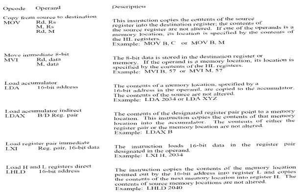
 8085 INSTRUCTION SET INSTRUCTION DETAILS DATA TRANSFER INSTRUCTIONS MOV Rd, Rs Copy from source to destination This instruction copies the contents of the source register Rs into the destination register
Microprocessors and Microcontrollers Prof. Santanu Chattopadhyay Department of E & EC Engineering Indian Institute of Technology, Kharagpur
 Microprocessors and Microcontrollers Prof. Santanu Chattopadhyay Department of E & EC Engineering Indian Institute of Technology, Kharagpur Lecture - 09 8085 Microprocessors (Contd.) (Refer Slide Time:
AE66/AC66/AT66/ AE108/AC108/AT108 MICROPROCESSORS & MICROCONTROLLERS
 Q.2 a. Draw pin diagram and signal group diagram of 8085 microprocessor. (8) b. List out the various categories of the 8085 instructions. Give examples of the instructions for each group. (8) Data transfer
MAHALAKSHMI ENGINEERING COLLEGE TIRUCHIRAPALLI
 MAHALAKSHMI ENGINEERING COLLEGE TIRUCHIRAPALLI-621213. QUESTION BANK DEPARTMENT: EEE SUB CODE: EE2324 YR/ SEM:III/ VI SUB NAME: MICROPROCESSORS & MICROCONTROLLERS UNIT 2- PROGRAMMING OF 8085 MICROPROCESSORS
The Purpose of Interrupt
 Interrupts 3 Introduction In this chapter, the coverage of basic I/O and programmable peripheral interfaces is expanded by examining a technique called interrupt-processed I/O. An interrupt is a hardware-initiated
This page intentionally left blank
 This page intentionally left blank Copyright 2010, 2006, New Age International (P) Ltd., Publishers Published by New Age International (P) Ltd., Publishers All rights reserved. No part of this ebook may
Interrupts. by Rahul Patel, Assistant Professor, EC Dept., Sankalchand Patel College of Engg.,Visnagar
 Chapter 12 Interrupts by Rahul Patel, Assistant Professor, EC Dept., Sankalchand Patel College of Engg.,Visnagar Microprocessor & Interfacing (140701) Rahul Patel 1 Points to be Discussed 8085 Interrupts
1-Operand instruction types 1 INC/ DEC/ NOT/NEG R/M. 2 PUSH/ POP R16/M16/SR/F 2 x ( ) = 74 opcodes 3 MUL/ IMUL/ DIV/ DIV R/M
 = 74 opcodes 3 MUL/ IMUL/ DIV/ DIV R/M") Increment R16 1-Operand instruction types 1 INC/ DEC/ NOT/NEG R/M 4 x (16+48) = 256 opcodes 2 PUSH/ POP R16/M16/SR/F 2 x (8+24+4+1) = 74 opcodes 3 MUL/ IMUL/ DIV/ DIV R/M 4 x (16+48) = 256 opcodes INC
Increment R16 1-Operand instruction types 1 INC/ DEC/ NOT/NEG R/M 4 x (16+48) = 256 opcodes 2 PUSH/ POP R16/M16/SR/F 2 x (8+24+4+1) = 74 opcodes 3 MUL/ IMUL/ DIV/ DIV R/M 4 x (16+48) = 256 opcodes INC
8086 Hardware Specification
 Content: Segment 5 8086 Hardware Specification 8086 Modes of operation. Pin diagram and pin function of 8086. 8284A Clock generator operation and pin functions. Prepared By: Mohammed Abdul Kader Lecturer,
G. Pullaiah College of Engineering and Technology: Kurnool Department Of Electronics and Communication Engineering
 G. Pullaiah College of Engineering and Technology: Kurnool Department Of Electronics and Communication Engineering LECTURE NOTES MICROPROCESSORS AND INTERFACING PREPARED BY V.SHANTHI ASST PROFESSOR DEPT