Memory & Simple I/O Interfacing
|
|
|
- Tracey Gallagher
- 5 years ago
- Views:
Transcription

1 Chapter 10 Memory & Simple I/O Interfacing Expected Outcomes Explain the importance of tri-state devices in microprocessor system Distinguish basic type of semiconductor memory and their applications Relate the address and data bus for various memories Describe I/O interfacing concept such as I/O driver and memory mapped Relate the role of latch and buffer in interfacing with simple I/O devices
2 Tri-state Devices Any devices connected to a microprocessor should configure in tristate This is because only one device can communicate with the processor at one time leaving other devices at high impedance Devices with tristate outputs have an enable input such as OE, CS, E, etc With this configuration, there will not be any devices fighting for control of common wire which may cause damaging to current flow Common devices connected to mp Address decoder Memory (ROM/RAM) Input devices such as keyboard, mouse, switch etc Output devices such as printer, monitor, LED, LCD
3 Tri-state Devices Lower address mp Upper address RAM ROM LED CS CS CS CS Address Decoder Chip selector
4 Memory
 Volatile type as data are lost as the power is off Temporary storage and")
5 Memory Memory system is used to store data and instruction Type of memory ROM (Read Only Memory) Nonvolatile data remains even the power is off Normally used to store vectors, self-test routine, monitor program, common subroutine and etc Special device is required to store program in ROM RAM (Random Access Memory) Volatile type as data are lost as the power is off Temporary storage and normally used for operation and application system
6 ROM Programmable Maskable ROM Very cheap and normally is programmed in factory for mass production One-time written and widely used in game cassette Programmable ROM (PROM) One-time written and can be programmed by using PROM programmer One-time PROM (OTPROM) Cheap version of PROM with plastic packed
7 ROM Flash Memory Like EEPROM, but erasing process involves block-by-block Common in digital camera & MP3 less expensive ROM PROM OTPROM EPROM EEPROM more expensive
 2764 8 kbyte (8192 x 8 bits) 27128 16 kbytes (16384 x 8 bits) 27256 32")
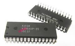
 2864 8 kbyte (8192 x 8 bits) Address bus A0 - An OE* CS* Vpp GND D0 - D7")
8 EPROM Common industrial EPROM kbyte (2048 x 8 bits) kbyte (4096 x 8 bits) kbyte (8192 x 8 bits) kbytes (16384 x 8 bits) kbytes (32768 x 8 bits) +5V Common industrial EEPROM kbyte (2048 x 8 bits) kbyte (8192 x 8 bits) Address bus A0 - An OE* CS* Vpp GND D0 - D7 Data bus
9 EPROM Part No Capacity Org Access Pins Vpp K 2Kx8 450ns 24 25V K 4Kx8 450ns 24 25V 27C K 4Kx8 450ns 24 25V CMOS K 8Kx8 200ns 28 21V 27C K 8Kx8 120ns V CMOS K 16Kx8 250ns 28 21V 27C K 32Kx8 150ns V CMOS 27C K 6Kx8 150ns V CMOS 27C K 128Kx8 150ns V CMOS 27C K 256Kx8 150ns V CMOS 27C K 512Kx8 150ns V CMOS
10 EEPROM & Flash Chip Some common EEPROM Part No Capacity Org Speed Pins Vpp 2816A-25 16K 2Kx8 250ns 24 5V 2864A 64K 8Kx8 250ns 28 5V 28C64A-25 64K 8Kx8 250ns 28 5V CMOS 28C K 32Kx8 150ns 28 5V Some common Flash Chips Part No Capacity Org Speed Pins Vpp 28F K 32Kx8 200ns 32 12V CMOS 28F K 128Kx8 150ns 32 12V CMOS 28F K 256Kx8 150ns 32 12V CMOS
11 EPROM Pin Function A0-An (Address Bus) Address bus directly connected to lower address of microprocessor D0-Dn (Data Bus) Data bus directly connected to data bus CS* (Chip Select) To activate EPROM and connected to address decoder OE* (Output Enable) ROM place data into data bus
12 EPROM Pin Function Vpp Used by EPROM programmer to change bit in the chip Place into high when it is not used CS* OE* Functions 1 0 IC disable with minimum power consumption 1 1 IC disable with minimum power consumption 0 0 Read mode; data are placed on data bus 0 1 Wait state mode; data are placed on the bus when OE* is activated
13 EPROM Memory Chip A7 A6 A5 A4 A3 A2 A1 A0 D0 D1 D2 GND A7 A6 A5 A4 A3 A2 A1 A0 D0 D1 D2 GND Vpp A12 A7 A6 A5 A4 A3 A2 A1 A0 D0 D1 D2 GND Vpp A12 A7 A6 A5 A4 A3 A2 A1 A0 D0 D1 D2 GND Vpp A12 A7 A6 A5 A4 A3 A2 A1 A0 D0 D1 D2 GND A15 A12 A7 A6 A5 A4 A3 A2 A1 A0 D0 D1 D2 GND Vcc A8 A9 A11 OE* A10 CE D7 D6 D5 D4 D3 Vcc A8 A9 A11 OE* A10 CE D7 D6 D5 D4 D3 Vcc PGM N.C A8 A9 A11 OE* A10 CE D7 D6 D5 D4 D3 Vcc PGM A13 A8 A9 A11 OE* A10 CE D7 D6 D5 D4 D3 Vcc A14 A13 A8 A9 A11 OE* A10 CE D7 D6 D5 D4 D3 Vcc A14 A13 A8 A9 A11 OE*/Vpp A10 CE D7 D6 D5 D4 D3 Examples of Parallel EPROMs
14 RAM Two basic types of RAM Static RAM (SRAM) Easy to be used and requires an internal flip-flop to store each bit Need 4 6 transistor for each FF and suitable for small system 4 times compact than SRAM with the same size Normally used in personal computer Dynamic RAM (DRAM) Cheaper as dynamic RAM uses a single transistor that acts like a charged capacitor to store each bit Since the charge leaks, a DRAM must use refresh circuit to recharge the capacitor periodically (typically every 2 ms)
15 RAM & NVRAM Performance difference DRAM contain more data per chip size SRAM is faster and simpler NV-RAM (Non-volatile RAM) is introduced to allow the CPU to read and write to it and not lost the content even the power is turned off To retain the content, the NVRAM chip internally Uses extremely power efficient CMOS Uses an internal lithium battery as backup energy Uses intelligent control circuitry to monitor Vcc pin and activates internal power if needed Thus the NV-RAM is expensive because it must provide the facilities in a single IC
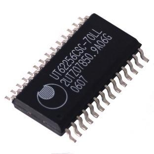
16 SRAM & DRAM Examples of SRAM & DRAM Part No Capacity Org Speed Pins Vpp 6116P-1 16K 2Kx8 100ns 24 CMOS 6116LP-3 16K 2Kx8 150ns 24 CMOS 6264P-10 64K 2Kx8 100ns 28 CMOS 62256LP K 32Kx8 100ns 28 Low Power CMOS 62256LP K 32Kx8 120ns 28 Low Power CMOS Part No Capacity Org Speed Pins K 64Kx1 150ns K 256Kx1 150ns P-8 1M 1Mx1 80ns 18

17 NVRAM NV-RAM from Dallas Semiconductor Part No Capacity Org Speed Pins DS1220Y K 2Kx8 150ns 26 DS1225AB K 8Kx8 150ns 28 DS1230Y K 32Kx8 85ns 28
18 RAM Common industrial RAM kbyte (2048 x 8 bits) 6164/ kbyte (8192 x 8 bits) 43256/ kbytes (32768 x 8 bits) +5V Address bus A0 - An D0 - D7 OE* CS* WE* GND Data bus
19 RAM A0-An (Address Bus) - Address bus directly connected to lower address of microprocessor D0-Dn (Data Bus) - Data bus directly connected to data bus CS* (Chip Select) - To activate EPROM and connected to address decoder OE* (Output Enable) - RAM places data into data bus WE* (Write Enable) - RAM stores data into cell
20 RAM The role of CS*, OE* and WE* CS* OE* WE* Functions 1 X X IC disable with minimum power consumption Undefined Read mode; data are placed on data bus Write mode; data are latched Wait state mode
21 2764 vs 6264 Vpp A12 A7 A6 A5 A4 A3 A2 A1 A0 D0 D1 D2 GND Vcc PGM* N.C A8 A9 A11 OE* A10 CE* D7 D6 D5 D4 D N.C A12 A7 A6 A5 A4 A3 A2 A1 A0 D0 D1 D2 GND Vcc WE* CS2 A8 A9 A11 OE* A10 CS1* D7 D6 D5 D4 D
22 Access Time The performance of memory chips normally are based on access time Access time (t ac ) is defined as time taken for the memory to place data onto the data bus as the read signal is received Address valid address CS* Data valid data t ac


23 Simple I/O Devices
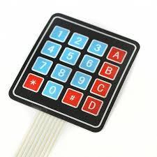
24 Input Devices Most input devices do not possess the tristate configuration Normally they are connected to other tristate devices such as buffer to ensure proper interface with mp Common input devices Switches (reset, SPST, SPDT etc) Keypad Sensors X1 X2 X3 X A B C * 0 # D Y1 Y2 Y3 Y4
25 Buffer Buffer is a circuit that allows any logics onto the data bus 74LS244 unidirectional tri-state buffer If OE=0, input is allowed to pass through If OE=1, output is placed in high impedance 74LS245 bidirectional buffer A.k.a transceiver Data direction is determined by DIR If DIR=0, data movement is from A to B If DIR=1, data movement is from B to A
26 Buffer Q0 Q1 Q2 Q3 Q4 Q5 Q6 Q D0 D1 D2 D3 D4 D5 D6 D LS244 OE1 OE B0 B1 B2 B3 B4 B5 B6 B A0 A1 A2 A3 A4 A5 A6 A LS245 DIR EN 1 19
27 Simple Input Interface Simple inputs connection with a buffer Enable pins (OE1* & OE2*) will activate the buffer and normally are connected to address decoder D8-D15 Q7 Q6 Q5 Q4 Q3 Q2 Q D7 D6 D5 D4 D3 D2 D1 +5V 1k 1k 1k 1k 1k 1k 1k 1k Q0 D0 OE1 OE2
28 Keypad Encoder When a keypad is used in a system, a keypad encoder (74922) is required to facilitate the program 74C922 X1 X2 X3 X A B C * 0 # D Y1 Y2 Y3 Y X1 X2 X3 X4 Y1 Y2 Y3 Y4 D0 D1 D2 D3 DA To mp LE OE 20 1
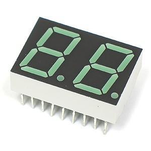
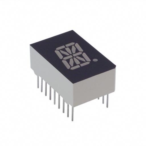
29 Output Devices Like input devices, output devices do not possess the tristate configuration They are connected to other tristate devices such as latch for proper interface with processor Common output devices Light Emitting Diode (LED) Seven Segment Display Dot Matrix f e a g d b c dp R1 R2 R3 R4 R5 R6 R7 R8 C1 C2 C3 C4 C5 C6 C7 C8
30 LED LED is the most common output device used in microprocessorbased system due its simplicity & cost +5V +5V '1' 330R '0' 330R '1' 330R '0' 330R
31 7-Segment Display There two type configurations Common Anode Common Cathode a b c d e f g dp +5V LATCH LATCH Common Anode Common Cathode
32 7-Segment Display Common Cathode Common Anode f a g b e d c dp
33 7-Segment Display Common Cathode f a g b e d c dp a b c d e f g a b c d e f g A B C D E F
34 Latch Latch is a circuit that capture value at the input 74LS373 transparent latch During LE=1, Q=D During LE=0, Q hold D during negative edge Another version is 74LS573 where the difference is in pin configuration 74LS374 edge triggering During positive transition at CP, data is transferred from D to Q Another version is 74LS574 where the difference is in pin configuration
35 Latch Q0 Q1 Q2 Q3 Q4 Q5 Q6 Q D0 D1 D2 D3 D4 D5 D6 D LS373 LE OE 11 1 Q0 Q1 Q2 Q3 Q4 Q5 Q6 Q D0 D1 D2 D3 D4 D5 D6 D LS374 CP OE 11 1 Q0 Q1 Q2 Q3 Q4 Q5 Q6 Q D0 D1 D2 D3 D4 D5 D6 D LS573 LE OE 20 1
36 Dot Matrix A multi-purpose output display, dot matrix is another common output device C1 C2 C3 C4 C5 C6 C7 C8 C1 R1 R2 R3 R4 R5 R6 R7 R8 R1 R2 R3 R4 R5 R6 R7 R8
37 Self-Test Determine the number of address pins and memory capacity of the following EPROM Part No Capacity (bytes) Address Pins TMS27C64 HD2716 NM27C LP-10 27C C
38 Self-Test Exercise For ROM chip 27128, find the number of data and address pins. In your opinion what is the minimum pin configuration of the chip Exercise Discuss the number of pins for addresses in (i) 2 kbytes RAM (ii) 512 bytes of RAM Exercise Explain the difference between EEPROM and flash memory Exercise Which memory is used as cache memory in the PC?
39 Self-Test Exercise Explain the role of OE*, CS*, WE* pins in RAM Exercise Why do we need to use latch instead of connecting the output device (such as 7-segment display) directly to the CPU? Exercise What is access time for a memory? Briefly describe the important of fast access time in a microprocessor system by giving an example
DIGITAL SYSTEM FUNDAMENTALS (ECE421) DIGITAL ELECTRONICS FUNDAMENTAL (ECE422)
 DIGITAL ELECTRONICS FUNDAMENTAL (ECE422)") COURSE / CODE DIGITAL SYSTEM FUNDAMENTALS (ECE421) DIGITAL ELECTRONICS FUNDAMENTAL (ECE422) Memory In computing, memory refers to the computer hardware devices used to store information for immediate use
COURSE / CODE DIGITAL SYSTEM FUNDAMENTALS (ECE421) DIGITAL ELECTRONICS FUNDAMENTAL (ECE422) Memory In computing, memory refers to the computer hardware devices used to store information for immediate use
8051 INTERFACING TO EXTERNAL MEMORY
 8051 INTERFACING TO EXTERNAL MEMORY Memory Capacity The number of bits that a semiconductor memory chip can store Called chip capacity It can be in units of Kbits (kilobits), Mbits (megabits), and so on
Address connections Data connections Selection connections
 Interface (cont..) We have four common types of memory: Read only memory ( ROM ) Flash memory ( EEPROM ) Static Random access memory ( SARAM ) Dynamic Random access memory ( DRAM ). Pin connections common
Basic Organization Memory Cell Operation. CSCI 4717 Computer Architecture. ROM Uses. Random Access Memory. Semiconductor Memory Types
 CSCI 4717/5717 Computer Architecture Topic: Internal Memory Details Reading: Stallings, Sections 5.1 & 5.3 Basic Organization Memory Cell Operation Represent two stable/semi-stable states representing
Computer Organization. 8th Edition. Chapter 5 Internal Memory
 William Stallings Computer Organization and Architecture 8th Edition Chapter 5 Internal Memory Semiconductor Memory Types Memory Type Category Erasure Write Mechanism Volatility Random-access memory (RAM)
Lecture Objectives. Introduction to Computing Chapter 0. Topics. Numbering Systems 04/09/2017
 Lecture Objectives Introduction to Computing Chapter The AVR microcontroller and embedded systems using assembly and c Students should be able to: Convert between base and. Explain the difference between
William Stallings Computer Organization and Architecture 8th Edition. Chapter 5 Internal Memory
 William Stallings Computer Organization and Architecture 8th Edition Chapter 5 Internal Memory Semiconductor Memory The basic element of a semiconductor memory is the memory cell. Although a variety of
UMBC. Select. Read. Write. Output/Input-output connection. 1 (Feb. 25, 2002) Four commonly used memories: Address connection ... Dynamic RAM (DRAM)
 Four commonly used memories: Address connection ... Dynamic RAM (DRAM)") Memory Types Two basic types: ROM: Read-only memory RAM: Read-Write memory Four commonly used memories: ROM Flash (EEPROM) Static RAM (SRAM) Dynamic RAM (DRAM) Generic pin configuration: Address connection
Memory Types Two basic types: ROM: Read-only memory RAM: Read-Write memory Four commonly used memories: ROM Flash (EEPROM) Static RAM (SRAM) Dynamic RAM (DRAM) Generic pin configuration: Address connection
Logic and Computer Design Fundamentals. Chapter 8 Memory Basics
 Logic and Computer Design Fundamentals Memory Basics Overview Memory definitions Random Access Memory (RAM) Static RAM (SRAM) integrated circuits Arrays of SRAM integrated circuits Dynamic RAM (DRAM) Read
Organization. 5.1 Semiconductor Main Memory. William Stallings Computer Organization and Architecture 6th Edition
 William Stallings Computer Organization and Architecture 6th Edition Chapter 5 Internal Memory 5.1 Semiconductor Main Memory 5.2 Error Correction 5.3 Advanced DRAM Organization 5.1 Semiconductor Main Memory
Chapter 5 Internal Memory
 Chapter 5 Internal Memory Memory Type Category Erasure Write Mechanism Volatility Random-access memory (RAM) Read-write memory Electrically, byte-level Electrically Volatile Read-only memory (ROM) Read-only
William Stallings Computer Organization and Architecture 6th Edition. Chapter 5 Internal Memory
 William Stallings Computer Organization and Architecture 6th Edition Chapter 5 Internal Memory Semiconductor Memory Types Semiconductor Memory RAM Misnamed as all semiconductor memory is random access
Concept of Memory. The memory of computer is broadly categories into two categories:
 Concept of Memory We have already mentioned that digital computer works on stored programmed concept introduced by Von Neumann. We use memory to store the information, which includes both program and data.
Microcontroller Systems. ELET 3232 Topic 11: General Memory Interfacing
 Microcontroller Systems ELET 3232 Topic 11: General Memory Interfacing 1 Objectives To become familiar with the concepts of memory expansion and the data and address bus To design embedded systems circuits
ECSE-2610 Computer Components & Operations (COCO)
") ECSE-2610 Computer Components & Operations (COCO) Part 18: Random Access Memory 1 Read-Only Memories 2 Why ROM? Program storage Boot ROM for personal computers Complete application storage for embedded
ECSE-2610 Computer Components & Operations (COCO) Part 18: Random Access Memory 1 Read-Only Memories 2 Why ROM? Program storage Boot ROM for personal computers Complete application storage for embedded
Introduction read-only memory random access memory
 Memory Interface Introduction Simple or complex, every microprocessorbased system has a memory system. Almost all systems contain two main types of memory: read-only memory (ROM) and random access memory
Contents. Main Memory Memory access time Memory cycle time. Types of Memory Unit RAM ROM
 Memory Organization Contents Main Memory Memory access time Memory cycle time Types of Memory Unit RAM ROM Memory System Virtual Memory Cache Memory - Associative mapping Direct mapping Set-associative
Overview. Memory Classification Read-Only Memory (ROM) Random Access Memory (RAM) Functional Behavior of RAM. Implementing Static RAM
 Random Access Memory (RAM) Functional Behavior of RAM. Implementing Static RAM") Memories Overview Memory Classification Read-Only Memory (ROM) Types of ROM PROM, EPROM, E 2 PROM Flash ROMs (Compact Flash, Secure Digital, Memory Stick) Random Access Memory (RAM) Types of RAM Static
Memories Overview Memory Classification Read-Only Memory (ROM) Types of ROM PROM, EPROM, E 2 PROM Flash ROMs (Compact Flash, Secure Digital, Memory Stick) Random Access Memory (RAM) Types of RAM Static
THE MICROCOMPUTER SYSTEM CHAPTER - 2
 THE MICROCOMPUTER SYSTEM CHAPTER - 2 20 2.1 GENERAL ASPECTS The first computer was developed using vacuum tubes. The computers thus developed were clumsy and dissipating more power. After the invention
COMP3221: Microprocessors and. and Embedded Systems. Overview. Lecture 23: Memory Systems (I)
") COMP3221: Microprocessors and Embedded Systems Lecture 23: Memory Systems (I) Overview Memory System Hierarchy RAM, ROM, EPROM, EEPROM and FLASH http://www.cse.unsw.edu.au/~cs3221 Lecturer: Hui Wu Session
COMP3221: Microprocessors and Embedded Systems Lecture 23: Memory Systems (I) Overview Memory System Hierarchy RAM, ROM, EPROM, EEPROM and FLASH http://www.cse.unsw.edu.au/~cs3221 Lecturer: Hui Wu Session
Internal Memory. Computer Architecture. Outline. Memory Hierarchy. Semiconductor Memory Types. Copyright 2000 N. AYDIN. All rights reserved.
 Computer Architecture Prof. Dr. Nizamettin AYDIN naydin@yildiz.edu.tr nizamettinaydin@gmail.com Internal Memory http://www.yildiz.edu.tr/~naydin 1 2 Outline Semiconductor main memory Random Access Memory
(Advanced) Computer Organization & Architechture. Prof. Dr. Hasan Hüseyin BALIK (5 th Week)
 Computer Organization & Architechture. Prof. Dr. Hasan Hüseyin BALIK (5 th Week)") + (Advanced) Computer Organization & Architechture Prof. Dr. Hasan Hüseyin BALIK (5 th Week) + Outline 2. The computer system 2.1 A Top-Level View of Computer Function and Interconnection 2.2 Cache Memory
+ (Advanced) Computer Organization & Architechture Prof. Dr. Hasan Hüseyin BALIK (5 th Week) + Outline 2. The computer system 2.1 A Top-Level View of Computer Function and Interconnection 2.2 Cache Memory
Memory Overview. Overview - Memory Types 2/17/16. Curtis Nelson Walla Walla University
 Memory Overview Curtis Nelson Walla Walla University Overview - Memory Types n n n Magnetic tape (used primarily for long term archive) Magnetic disk n Hard disk (File, Directory, Folder) n Floppy disks
Computer Organization and Assembly Language (CS-506)
") Computer Organization and Assembly Language (CS-506) Muhammad Zeeshan Haider Ali Lecturer ISP. Multan ali.zeeshan04@gmail.com https://zeeshanaliatisp.wordpress.com/ Lecture 2 Memory Organization and Structure
Computer Organization and Assembly Language (CS-506) Muhammad Zeeshan Haider Ali Lecturer ISP. Multan ali.zeeshan04@gmail.com https://zeeshanaliatisp.wordpress.com/ Lecture 2 Memory Organization and Structure
Grundlagen Microcontroller Memory. Günther Gridling Bettina Weiss
 Grundlagen Microcontroller Memory Günther Gridling Bettina Weiss 1 Lecture Overview Memory Memory Types Address Space Allocation 2 Memory Requirements What do we want to store? program constants (e.g.
Unit 6 1.Random Access Memory (RAM) Chapter 3 Combinational Logic Design 2.Programmable Logic
 Chapter 3 Combinational Logic Design 2.Programmable Logic") EE 200: Digital Logic Circuit Design Dr Radwan E Abdel-Aal, COE Unit 6.Random Access Memory (RAM) Chapter 3 Combinational Logic Design 2. Logic Logic and Computer Design Fundamentals Part Implementation
EE 200: Digital Logic Circuit Design Dr Radwan E Abdel-Aal, COE Unit 6.Random Access Memory (RAM) Chapter 3 Combinational Logic Design 2. Logic Logic and Computer Design Fundamentals Part Implementation
Embedded Systems Design: A Unified Hardware/Software Introduction. Outline. Chapter 5 Memory. Introduction. Memory: basic concepts
 Hardware/Software Introduction Chapter 5 Memory Outline Memory Write Ability and Storage Permanence Common Memory Types Composing Memory Memory Hierarchy and Cache Advanced RAM 1 2 Introduction Memory:
Embedded Systems Design: A Unified Hardware/Software Introduction. Chapter 5 Memory. Outline. Introduction
 Hardware/Software Introduction Chapter 5 Memory 1 Outline Memory Write Ability and Storage Permanence Common Memory Types Composing Memory Memory Hierarchy and Cache Advanced RAM 2 Introduction Embedded
CREATED BY M BILAL & Arslan Ahmad Shaad Visit:
 CREATED BY M BILAL & Arslan Ahmad Shaad Visit: www.techo786.wordpress.com Q1: Define microprocessor? Short Questions Chapter No 01 Fundamental Concepts Microprocessor is a program-controlled and semiconductor
Keywords: NVSRAM, DRAM, SRAM, EEPROM, shadow RAM, NV Memory, MK48Z08, MK48Z18, nvsrams, NV SRAMs
 Maxim > Design Support > Technical Documents > Application Notes > Memory > APP 540 Keywords: NVSRAM, DRAM, SRAM, EEPROM, shadow RAM, NV Memory, MK48Z08, MK48Z18, nvsrams, NV SRAMs APPLICATION NOTE 540
Chapter 2: Fundamentals of a microprocessor based system
 Chapter 2: Fundamentals of a microprocessor based system Objectives Learn about the basic structure of microprocessor systems Learn about the memory read/write timing diagrams. Learn about address decoding
Components of a personal computer
 Components of a personal computer Computer systems ranging from a controller in a microwave oven to a large supercomputer contain components providing five functions. A typical personal computer has hard,
Module 5a: Introduction To Memory System (MAIN MEMORY)
") Module 5a: Introduction To Memory System (MAIN MEMORY) R E F E R E N C E S : S T A L L I N G S, C O M P U T E R O R G A N I Z A T I O N A N D A R C H I T E C T U R E M O R R I S M A N O, C O M P U T E
Module 5a: Introduction To Memory System (MAIN MEMORY) R E F E R E N C E S : S T A L L I N G S, C O M P U T E R O R G A N I Z A T I O N A N D A R C H I T E C T U R E M O R R I S M A N O, C O M P U T E
UNIT V (PROGRAMMABLE LOGIC DEVICES)
") UNIT V (PROGRAMMABLE LOGIC DEVICES) Introduction There are two types of memories that are used in digital systems: Random-access memory(ram): perform both the write and read operations. Read-only memory(rom):
UNIT V (PROGRAMMABLE LOGIC DEVICES) Introduction There are two types of memories that are used in digital systems: Random-access memory(ram): perform both the write and read operations. Read-only memory(rom):
Design with Microprocessors
 Design with Microprocessors Year III Computer Sci. English 1-st Semester Lecture 12: Memory interfacing Typical Memory Hierarchy [1] On-Chip Components Control edram Datapath RegFile ITLB DTLB Instr Data
Allmost all systems contain two main types of memory :
 Memory Interface Allmost all systems contain two main types of memory : read-only memory (ROM) system software and permanent system data random access memory (RAM) or read/write memory application software
Design with Microprocessors
 Design with Microprocessors Year III Computer Sci. English 1-st Semester Lecture 12: Memory interfacing Typical Memory Hierarchy [1] On-Chip Components Control edram Datapath RegFile ITLB DTLB Instr Data
Read Only Memory ROM
 Read Only Memory ROM A read only memory have address inputs and data outputs With m address lines you can access the 2 m different memory addresses At each address, there is one data word with n bits Usually,
ECE 341. Lecture # 16
 ECE 341 Lecture # 16 Instructor: Zeshan Chishti zeshan@ece.pdx.edu November 24, 2014 Portland State University Lecture Topics The Memory System Basic Concepts Semiconductor RAM Memories Organization of
Memory Pearson Education, Inc., Hoboken, NJ. All rights reserved.
 1 Memory + 2 Location Internal (e.g. processor registers, cache, main memory) External (e.g. optical disks, magnetic disks, tapes) Capacity Number of words Number of bytes Unit of Transfer Word Block Access
MEMORY BHARAT SCHOOL OF BANKING- VELLORE
 A memory is just like a human brain. It is used to store data and instructions. Computer memory is the storage space in computer where data is to be processed and instructions required for processing are
Semiconductor Memories: RAMs and ROMs
 Semiconductor Memories: RAMs and ROMs Lesson Objectives: In this lesson you will be introduced to: Different memory devices like, RAM, ROM, PROM, EPROM, EEPROM, etc. Different terms like: read, write,
Menu. word size # of words byte = 8 bits
 Menu LSI Components >Random Access Memory (RAM) Static RAM (SRAM) Dynamic RAM (DRAM) Read-Only Memory (ROM) Look into my... See figures from Lam text on web: RAM_ROM_ch6.pdf 1 It can be thought of as 1
EE 308: Microcontrollers
 EE 308: Microcontrollers AVR Architecture Aly El-Osery Electrical Engineering Department New Mexico Institute of Mining and Technology Socorro, New Mexico, USA January 23, 2018 Aly El-Osery (NMT) EE 308:
Memory and Programmable Logic
 Memory and Programmable Logic Memory units allow us to store and/or retrieve information Essentially look-up tables Good for storing data, not for function implementation Programmable logic device (PLD),
UMBC D 7 -D. Even bytes 0. 8 bits FFFFFC FFFFFE. location in addition to any 8-bit location. 1 (Mar. 6, 2002) SX 16-bit Memory Interface
 SX 16-bit Memory Interface") 8086-80386SX 16-bit Memory Interface These machines differ from the 8088/80188 in several ways: The data bus is 16-bits wide. The IO/M pin is replaced with M/IO (8086/80186) and MRDC and MWTC for 80286
8086-80386SX 16-bit Memory Interface These machines differ from the 8088/80188 in several ways: The data bus is 16-bits wide. The IO/M pin is replaced with M/IO (8086/80186) and MRDC and MWTC for 80286
Computer Memory. Textbook: Chapter 1
 Computer Memory Textbook: Chapter 1 ARM Cortex-M4 User Guide (Section 2.2 Memory Model) STM32F4xx Technical Reference Manual: Chapter 2 Memory and Bus Architecture Chapter 3 Flash Memory Chapter 36 Flexible
MODULE 12 APPLICATIONS OF MEMORY DEVICES:
 Introduction to Digital Electronic Design, Module 12 Application of Memory Devices 1 MODULE 12 APPLICATIONS OF MEMORY DEVICES: CONCEPT 12-1: REVIEW OF HOW MEMORY DEVICES WORK Memory consists of two parts.
Sir Sadiq s computer notes for class IX. Chapter no 4. Storage Devices
 17 Q: Define Computer memory or storage. Ans: Memory: Memory refers to the place where data is kept for later use. For example, a human being has a memory where he/she stores the things that can be recalled
Read and Write Cycles
 Read and Write Cycles The read cycle is shown. Figure 41.1a. The RAS and CAS signals are activated one after the other to latch the multiplexed row and column addresses respectively applied at the multiplexed
eaymanelshenawy.wordpress.com
 Lectures on Memory Interface Designed and Presented by Dr. Ayman Elshenawy Elsefy Dept. of Systems & Computer Eng.. Al-Azhar University Email : eaymanelshenawy@yahoo.com eaymanelshenawy.wordpress.com Lecture
UNIT:4 MEMORY ORGANIZATION
 1 UNIT:4 MEMORY ORGANIZATION TOPICS TO BE COVERED. 4.1 Memory Hierarchy 4.2 Memory Classification 4.3 RAM,ROM,PROM,EPROM 4.4 Main Memory 4.5Auxiliary Memory 4.6 Associative Memory 4.7 Cache Memory 4.8
 Chapter 1 Microprocessor architecture ECE 3120 Dr. Mohamed Mahmoud http://iweb.tntech.edu/mmahmoud/ mmahmoud@tntech.edu Outline 1.1 Computer hardware organization 1.1.1 Number System 1.1.2 Computer hardware
Picture of memory. Word FFFFFFFD FFFFFFFE FFFFFFFF
 Memory Sequential circuits all depend upon the presence of memory A flip-flop can store one bit of information A register can store a single word, typically 32-64 bits Memory allows us to store even larger
TUTORIAL Describe the circumstances that would prompt you to use a microprocessorbased design solution instead of a hard-wired IC logic design.
 TUTORIAL 1 1. Make a list of 10 products containing microprocessors that we use everyday. Personal computer Television Calculator Elevator Mobile phones MP3 players Microwave ovens DVD players Engine Control
CS 265. Computer Architecture. Wei Lu, Ph.D., P.Eng.
 CS 265 Computer Architecture Wei Lu, Ph.D., P.Eng. Part 4: Memory Organization Our goal: understand the basic types of memory in computer understand memory hierarchy and the general process to access memory
RISC (Reduced Instruction Set Computer)
") RISC (Reduced Instruction Set Computer) Reduced Instruction Set Computing (RISC), is a microprocessor CPU design philosophy that favors a smaller and simpler set of instructions that all take about the
RISC (Reduced Instruction Set Computer) Reduced Instruction Set Computing (RISC), is a microprocessor CPU design philosophy that favors a smaller and simpler set of instructions that all take about the
Chapter 4 Main Memory
 Chapter 4 Main Memory Course Outcome (CO) - CO2 Describe the architecture and organization of computer systems Program Outcome (PO) PO1 Apply knowledge of mathematics, science and engineering fundamentals
Memory memories memory
 Memory Organization Memory Hierarchy Memory is used for storing programs and data that are required to perform a specific task. For CPU to operate at its maximum speed, it required an uninterrupted and
Design and Implementation of an AHB SRAM Memory Controller
 Design and Implementation of an AHB SRAM Memory Controller 1 Module Overview Learn the basics of Computer Memory; Design and implement an AHB SRAM memory controller, which replaces the previous on-chip
Interface DAC to a PC. Control Word of MC1480 DAC (or DAC 808) 8255 Design Example. Engineering 4862 Microprocessors
 8255 Design Example. Engineering 4862 Microprocessors") Interface DAC to a PC Engineering 4862 Microprocessors Lecture 22 Cheng Li EN-4012 licheng@engr.mun.ca DAC (Digital-to-Analog Converter) Device used to convert digital pulses to analog signals Two methods
Interface DAC to a PC Engineering 4862 Microprocessors Lecture 22 Cheng Li EN-4012 licheng@engr.mun.ca DAC (Digital-to-Analog Converter) Device used to convert digital pulses to analog signals Two methods
COMP2121: Microprocessors and Interfacing. Introduction to Microprocessors
 COMP2121: Microprocessors and Interfacing Introduction to Microprocessors http://www.cse.unsw.edu.au/~cs2121 Lecturer: Hui Wu Session 2, 2017 1 1 Contents Processor architectures Bus Memory hierarchy 2
Memory Interfacing & decoding. Intel CPU s
 Memory Interfacing & decoding in Intel CPU s Outline Address decoding Chip select Memory configurations Minimum Mode - - A19 - A19 - Simplified Drawing of 8088 Minimum Mode MEMORY MEMW When Memory is selected?
Microprocessor Architecture. mywbut.com 1
 Microprocessor Architecture mywbut.com 1 Microprocessor Architecture The microprocessor can be programmed to perform functions on given data by writing specific instructions into its memory. The microprocessor
ORG ; Week8. Memory and Memory Interfacing
 Dec 10 Hex A Bin 00001010 ORG ; Week8 Memory and Memory Interfacing OBJECTIVES this chapter enables the student to: Define the terms capacity, organization, and speed as used in semiconductor memories.
Memory and Programmable Logic
 Digital Circuit Design and Language Memory and Programmable Logic Chang, Ik Joon Kyunghee University Memory Classification based on functionality ROM : Read-Only Memory RWM : Read-Write Memory RWM NVRWM
CS 320 February 2, 2018 Ch 5 Memory
 CS 320 February 2, 2018 Ch 5 Memory Main memory often referred to as core by the older generation because core memory was a mainstay of computers until the advent of cheap semi-conductor memory in the
Summer 2003 Lecture 18 07/09/03
 Summer 2003 Lecture 18 07/09/03 NEW HOMEWORK Instruction Execution Times: The 8088 CPU is a synchronous machine that operates at a particular clock frequency. In the case of the original IBM PC, that clock
CS429: Computer Organization and Architecture
 CS429: Computer Organization and Architecture Dr. Bill Young Department of Computer Sciences University of Texas at Austin Last updated: November 28, 2017 at 14:31 CS429 Slideset 18: 1 Random-Access Memory
Unit 5 DOS INTERRPUTS
 Unit 5 DOS INTERRPUTS 5.1 Introduction The DOS (Disk Operating System) provides a large number of procedures to access devices, files and memory. These procedures can be called in any user program using
CS429: Computer Organization and Architecture
 CS429: Computer Organization and Architecture Dr. Bill Young Department of Computer Sciences University of Texas at Austin Last updated: April 9, 2018 at 12:16 CS429 Slideset 17: 1 Random-Access Memory
machine cycle, the CPU: (a) Fetches an instruction, (b) Decodes the instruction, (c) Executes the instruction, and (d) Stores the result.
 Fetches an instruction, (b) Decodes the instruction, (c) Executes the instruction, and (d) Stores the result.") Central Processing Unit (CPU) A processor is also called the CPU, and it works hand in hand with other circuits known as main memory to carry out processing. The CPU is the "brain" of the computer; it
Central Processing Unit (CPU) A processor is also called the CPU, and it works hand in hand with other circuits known as main memory to carry out processing. The CPU is the "brain" of the computer; it
Chapter TEN. Memory and Memory Interfacing
 Chapter TEN Memory and Memory Interfacing OBJECTIVES this chapter enables the student to: Define the terms capacity, organization, and speed as used in semiconductor memories. Calculate the chip capacity
ET2640. Unit 5:ADVANCED I/O TECHNIQUES Pearson Education, Inc. Pearson Prentice Hall Upper Saddle River, NJ 07458
 ET2640 Unit 5:ADVANCED I/O TECHNIQUES skong@itt-tech.edu HARDWARE CONNECTION CHAPTER 8 8051 PINOUT XTAL1 & XTAL2 On-chip oscillator requires an external clock Quartz crystal clock 2 external 30 pf capacitors
UNIT-V MEMORY ORGANIZATION
 UNIT-V MEMORY ORGANIZATION 1 The main memory of a computer is semiconductor memory.the main memory unit is basically consists of two kinds of memory: RAM (RWM):Random access memory; which is volatile in
chapter 8 The Memory System Chapter Objectives
 chapter 8 The Memory System Chapter Objectives In this chapter you will learn about: Basic memory circuits Organization of the main memory Memory technology Direct memory access as an I/O mechanism Cache
M. Sc (CS) (II Semester) Examination, Subject: Computer System Architecture Paper Code: M.Sc-CS-203. Time: Three Hours] [Maximum Marks: 60
![M. Sc (CS) (II Semester) Examination, Subject: Computer System Architecture Paper Code: M.Sc-CS-203. Time: Three Hours] [Maximum Marks: 60](/thumbs/87/96339673.jpg "M. Sc (CS) (II Semester) Examination, Subject: Computer System Architecture Paper Code: M.Sc-CS-203. Time: Three Hours] [Maximum Marks: 60") M. Sc (CS) (II Semester) Examination, 2012-13 Subject: Computer System Architecture Paper Code: M.Sc-CS-203 Time: Three Hours] [Maximum Marks: 60 Note: Question Number 1 is compulsory. Answer any four
M. Sc (CS) (II Semester) Examination, 2012-13 Subject: Computer System Architecture Paper Code: M.Sc-CS-203 Time: Three Hours] [Maximum Marks: 60 Note: Question Number 1 is compulsory. Answer any four
Large and Fast: Exploiting Memory Hierarchy
 CSE 431: Introduction to Operating Systems Large and Fast: Exploiting Memory Hierarchy Gojko Babić 10/5/018 Memory Hierarchy A computer system contains a hierarchy of storage devices with different costs,
1. INTRODUCTION TO MICROPROCESSOR AND MICROCOMPUTER ARCHITECTURE:
 1. INTRODUCTION TO MICROPROCESSOR AND MICROCOMPUTER ARCHITECTURE: A microprocessor is a programmable electronics chip that has computing and decision making capabilities similar to central processing unit
ELCT 912: Advanced Embedded Systems
 Advanced Embedded Systems Lecture 2: Memory and Programmable Logic Dr. Mohamed Abd El Ghany, Memory Random Access Memory (RAM) Can be read and written Static Random Access Memory (SRAM) Data stored so
CPEG300 Embedded System Design. Lecture 3 Memory
 CPEG300 Embedded System Design Lecture 3 Memory Hamad Bin Khalifa University, Spring 2018 Review Von Neumann vs. Harvard architecture? System on Board, system on chip? Generic Hardware Architecture of
Memory and Programmable Logic
 Memory and Programmable Logic Mano & Ciletti Chapter 7 By Suleyman TOSUN Ankara University Outline RAM Memory decoding Error detection and correction ROM Programmable Logic Array (PLA) Programmable Array
Three-box Model: These three boxes need interconnecting (usually done by wiring known as a bus. 1. Processor CPU e.g. Pentium 4 2.
 Three-box Model: 1. Processor CPU e.g. Pentium 4 2. Storage - Memory 3. I/O input/output electronics for communication with other devices These three boxes need interconnecting (usually done by wiring
Memory Expansion. Lecture Embedded Systems
 Memory Expansion Lecture 22 22-1 In These Notes... Memory Types Memory Expansion Interfacing Parallel Serial Direct Memory Access controllers 22-2 Memory Characteristics and Issues Volatility - Does it
SECTION-A
 M.Sc(CS) ( First Semester) Examination,2013 Digital Electronics Paper: Fifth ------------------------------------------------------------------------------------- SECTION-A I) An electronics circuit/ device
MicroProcessor. MicroProcessor. MicroProcessor. MicroProcessor
 1 2 A microprocessor is a single, very-large-scale-integration (VLSI) chip that contains many digital circuits that perform arithmetic, logic, communication, and control functions. When a microprocessor
Sistemas Digitais I LESI - 2º ano
 Sistemas Digitais I LESI - 2º ano Lesson 9 - Memory, CPLDs and FPGAs Prof. João Miguel Fernandes (miguel@di.uminho.pt) Dept. Informática UNIVERSIDADE DO MINHO ESCOLA DE ENGENHARIA - Memory - Any sequential
Chapter 5. Internal Memory. Yonsei University
 Chapter 5 Internal Memory Contents Main Memory Error Correction Advanced DRAM Organization 5-2 Memory Types Memory Type Category Erasure Write Mechanism Volatility Random-access memory(ram) Read-write
System Unit. By: Khadeeja Farkash
 System Unit By: Khadeeja Farkash Objectives - What s a system unit? - What are the components of the system unit and explain their usage? - How does the processor work? - What are the similarities between
k -bit address bus n-bit data bus Control lines ( R W, MFC, etc.)
") THE MEMORY SYSTEM SOME BASIC CONCEPTS Maximum size of the Main Memory byte-addressable CPU-Main Memory Connection, Processor MAR MDR k -bit address bus n-bit data bus Memory Up to 2 k addressable locations
THE MEMORY SYSTEM SOME BASIC CONCEPTS Maximum size of the Main Memory byte-addressable CPU-Main Memory Connection, Processor MAR MDR k -bit address bus n-bit data bus Memory Up to 2 k addressable locations
Lecture (01) Introducing Embedded Systems and the Microcontrollers By: Dr. Ahmed ElShafee
 Introducing Embedded Systems and the Microcontrollers By: Dr. Ahmed ElShafee") Lecture (01) Introducing Embedded Systems and the Microcontrollers By: Dr. Ahmed ElShafee ١ Agenda What is microprocessor system? What is Microcontroller/embedded system? Definition of Embedded Systems
Lecture (01) Introducing Embedded Systems and the Microcontrollers By: Dr. Ahmed ElShafee ١ Agenda What is microprocessor system? What is Microcontroller/embedded system? Definition of Embedded Systems
Memories. Design of Digital Circuits 2017 Srdjan Capkun Onur Mutlu.
 Memories Design of Digital Circuits 2017 Srdjan Capkun Onur Mutlu http://www.syssec.ethz.ch/education/digitaltechnik_17 Adapted from Digital Design and Computer Architecture, David Money Harris & Sarah
! Memory Overview. ! ROM Memories. ! RAM Memory " SRAM " DRAM. ! This is done because we can build. " large, slow memories OR
 ESE 57: Digital Integrated Circuits and VLSI Fundamentals Lec 2: April 5, 26 Memory Overview, Memory Core Cells Lecture Outline! Memory Overview! ROM Memories! RAM Memory " SRAM " DRAM 2 Memory Overview
Contents. Memory System Overview Cache Memory. Internal Memory. Virtual Memory. Memory Hierarchy. Registers In CPU Internal or Main memory
 Memory Hierarchy Contents Memory System Overview Cache Memory Internal Memory External Memory Virtual Memory Memory Hierarchy Registers In CPU Internal or Main memory Cache RAM External memory Backing
Random Access Memory (RAM)
") Best known form of computer memory. "random access" because you can access any memory cell directly if you know the row and column that intersect at that cell. CS1111 CS5020 - Prof J.P. Morrison UCC 33
Best known form of computer memory. "random access" because you can access any memory cell directly if you know the row and column that intersect at that cell. CS1111 CS5020 - Prof J.P. Morrison UCC 33
I/O Design. Input / Output Instructions. Engineering 4862 Microprocessors. Lecture 23. Cheng Li
 Engineering 4862 Microprocessors Lecture 23 Cheng Li EN-4012 licheng@engr.mun.ca I/O Design When designing an I/O port, ensure that the port is only active when selected by the microprocessor Use latches
Computer Structure. Unit 2: Memory and programmable devices
 Computer Structure Unit 2: Memory and programmable devices Translated from Francisco Pérez García (fperez at us.es) by Mª Carmen Romero (mcromerot at us.es, Office G1.51, 954554324) Electronic Technology
Computer System Overview
 Computer System Overview based on CBSE curriculum Class 11 By- Neha Tyagi PGT CS KV 5 Jaipur II Shift, Jaipur Region Neha Tyagi, KV 5 Jaipur II Shift Introduction Computer is a machine which brought resolution
Memory classification:- Topics covered:- types,organization and working
 Memory classification:- Topics covered:- types,organization and working 1 Contents What is Memory? Cache Memory PC Memory Organisation Types 2 Memory what is it? Usually we consider this to be RAM, ROM
CSEE 3827: Fundamentals of Computer Systems. Storage
 CSEE 387: Fundamentals of Computer Systems Storage The big picture General purpose processor (e.g., Power PC, Pentium, MIPS) Internet router (intrusion detection, pacet routing, etc.) WIreless transceiver