An Overview of Standard Cell Based Digital VLSI Design
|
|
|
- Nigel Lawrence
- 5 years ago
- Views:
Transcription


1 An Overview of Standard Cell Based Digital VLSI Design With examples taken from the implementation of the 36-core AsAP1 chip and the 1000-core KiloCore chip Zhiyi Yu, Tinoosh Mohsenin, Aaron Stillmaker, Bevan Baas VCL Laboratory, UC Davis
2 Outline Overview of standard cellbased design Design of the AsAP1 and KiloCore chips including CAD Tool Flow
3 Standard cell vs. Full-custom IC design Standard-cell based IC design Design using standard cells Standard cells come from library provider Many different choices for cell size, delay, leakage power Many EDA tools to automate this flow Shorter design time Custom IC design (e.g., magic) Design all by yourself Higher performance Lower energy per workload (lower power) Smaller chip area
4 Standard cell based VLSI design flow Front end System specification and architecture HDL (verilog or VHDL) coding Behavioral simulations using RTL (HDL) Synthesis Gate-level simulations Back end Floorplanning, Power grid design Standard-cell Placement Interconnect routing DRC (Design Rule Check) LVS (Layout vs Schematic) Dynamic simulation and static timing analysis
5 Outline Overview of standard cell-based design Design of the AsAP1 and KiloCore chips including CAD Tool Flow
6 AsAP1 Block Diagram GALS array of identical processors Each processor is a reduced complexity programmable DSP with small memories Each processor can receive data from any two neighbors and send data to any of its four neighbors FIFO 0 32 words FIFO 1 32 words IMem 64 words ALU MAC Control DMem 128 words OSC Output Static config Dynamic config B. Baas 6
7 KiloCore Developed by the VLSI Computation Laboratory at UC Davis, with a similar architecture to AsAP (Asynchronous Array of Processors) A processing chip containing multiple uniform simple processor elements Globally Asynchronous Locally Synchronous (GALS) Each processor has its local clock generator Each processor can communicate with its neighbor processors using dual-clock FIFOs
8 KiloCore Design Contains 1,000 processors on one chip Fastest clock rate processor designed at a university 12 memories containing 64 KB each for 768 KB of shared memory 8 KiloCore Block Diagram Single Processor One 64 KB memory
9 Simple Diagram of the Front-End Design Flow System Specification RTL Coding Synthesis Gate level code Example: c =!a & b INV (.in(a),.out(a_inv)); AND (.in1 (a_inv),.in2(b),.out(c)); a b C
10 Simple diagram of the Back-end design flow gate level Verilog from synthesis Place & Route Final layout (go for fabrication) Gate level Verilog DRC LVS Design rule check Layout vs. schematic Timing information Gate level dynamic and/or static analysis


11 Back-End: Physical Design Flow
12 Back-end design of AsAP1 Technology: TSMC 0.18 μm CMOS Standard cell library: Artisan Tools Synthesis: Synopsis Design compiler Placement & Route: Cadence Encounter DRC & LVS: Mentor Calibre Static timing analysis: Primetime
13 Back-End Design of KiloCore Technology: IBM 32 nm PD-SOI CMOS Standard cell library: ARM-Artisan Tools Synthesis: Synopsis Design compiler Placement & Route: Cadence Encounter DRC & LVS: Mentor Calibre Static timing analysis: Primetime and UltraSim (Spice)
14 Flow of Placement and Routing Import needed files Floorplan Placement & in-place optimization Clock tree generation Routing
15 Import Needed Files Gate-level verilog (.v) Geometry information (.lef) Timing information (.lib) INV (.in (a),.out (a_inv)); AND (.in1 (a_inv),.in2 (b),.out (c)); INV: 1um width AND: 2 um width a INV b AND C INV: 1ns delay; AND: 2 ns delay Delay (a c): 1ns + 2ns = 3ns
16 Floorplan Size of chip Location of Pins Location of main blocks Power supply: give enough power for each gate Power supply (1.8 V) 1.75 V current 1.7 V Vdd (Metal) (need another power stripe) 1.65 V Gate 1 Gate 2 Gate 3 Gate 4 Gnd Voltage drop equation: V2 = V1 I * R

17 Floorplan of a single processor Inst Mem Data Mem ALU MAC Control Clock InFIFO 0 InFIFO 0

18 Floorplan of Single KiloCore Processor 18
19 Placement & In-Place Optimization Placement: place the gates (standard cells) Utilizes a long series of very complex optimizations to meet all design goals as best as possible. Design goals include: maximum delay of all paths, minimize length of all wires (to increase probability of a successful route), etc. In-place optimization Why: there will always be a timing difference between synthesis and layout (e.g., actual wire delay is different than predicted) How: change gate size, insert buffers May not change the circuit function!!

20 Placement of a single AsAP1 processor

21 Placement of Single KiloCore Processor 21


22 Placement of Single KiloCore Processor 22
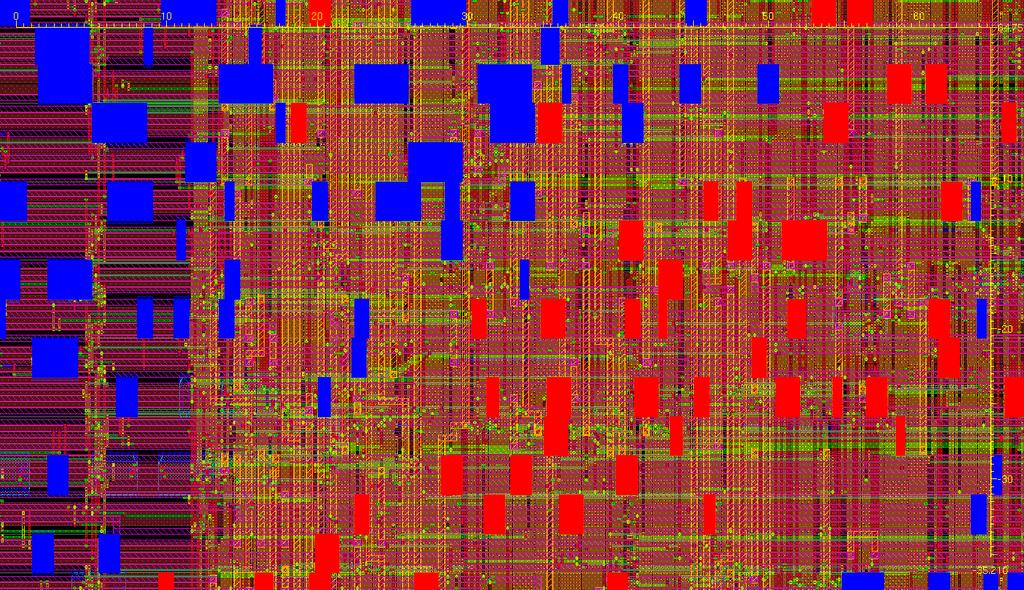
23 Clock Tree Design Main parameters: skew, delay, transition time Clock Delay= x S SET Q Clock Skew= x -y R CLR SQS SET SET Q Q R R CLR Q Q CLR Original Clock S SET Q R CLR SQS SET SET Q Q R R CLR Q Q CLR S SET Q R CLR SQS SET SET Q Q Clock Delay = y R R CLR Q Q CLR

24 Clock tree of a single AsAP1 processor

25 Clock Tree of a Single KiloCore Processor Colors indicate clock phase which is the same as clock skew 25
26 Routing Routing is the second step in the Standard Cell Place & Route process and consists of the CAD P&R tool routing all necessary signal wires Local power and ground connections to standard cells are made during an earlier power striping step and are made by a much simpler process of simply laying down horizontal power stripes Routing consists of two main steps Connection of global signals (power) Connect other signals


27 Metal Layer Topology Routing

28 Layout of a Single AsAP1 Processor After Routing Area: 0.8mm x 0.8mm

29 Layout of the first generation 6x6 AsAP1 Area: 30 mm^2 in 180 nm CMOS - 36 processors PADs One processor

30 Routing on a Single KiloCore Processor 239 μm x μm 574,733 transistors 30

31 KiloCore Chip Layout KiloCore Chip Entire chip takes up 8 mm x 8 mm or 64 mm 2 LVDS pairs used for high speed data I/O Drivers connected through C4 bump array I/O Drivers Single Processor 31 KiloCore Chip Layout SRAM Memories
32 Verification after layout DRC (design rule check) LVS (layout vs. schematic) GDS-II vs. (verilog + spice module) Gate level verilog dynamic simulation Mainly check the function Different with synthesis result
33 Useful tools Dynamic Simulation: Modelsim (Mentor), NC-verilog (Cadence), Active-HDL Synthesis: Design-compiler, design-analyzer (Synopsys) Placement & Routing Encounter & Virtuoso (Cadence) Astro (Synopsys) DRC & LVS Calibre (Mentor) Dracula (Cadence) Static Analysis Primetime (Synsopsys)
: Typical application 32 mw Typical 100% active 84 mw Power (1 Proc @ 0.9V, 116 MHz): Typical application 2.")
34 Chip Micrograph of the 36-Core AsAP1 IMem OSC Single Processor DMem FIFOs Flow: Standard-cell based Technology: TSMC 0.18 µm Transistors: 1 Proc 230,000 Chip 8.5 million Max speed: V Area: 1 Proc 0.66 mm² Chip 32.1 mm² Power (1 1.8V, 475 MHz): Typical application 32 mw Typical 100% active 84 mw Power (1 0.9V, 116 MHz): Typical application 2.4 mw ISSCC 2006 HotChips 2006 IEEE Micro 2007 JSSC

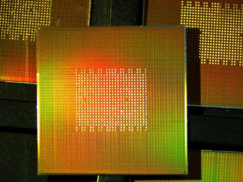
35 KiloCore Chip Technology 32nm IBM PDSOI CMOS 8 mm 7.82 mm Processors Indep. Mems Num. Oscs per chip V 1.24 GHz, V 115 MHz, V 12 per chip Die Area 64 mm 2 Array Area 60 mm mm 8 mm Transistors C4 Bumps Package 621 Million 564 (162 I/O) 676 Pad Flip-Chip BGA Slide 35 HotChips 2016
36
37 KiloCore Measurements A maximum of 1.78 trillion instructions per second Assuming a custom package design Processors achieve their optimal energy times time of 11.1 (pj x ns / instruction) at 0.9 V Supply Voltage Max Clock Freq (MHz) Total Chip Instructions / sec At minimum voltage, KiloCore can perform 115 billion instructions per second using 0.7 Watts low enough to be powered by a single AA battery! Total Chip Power 1.10 V Trillion 39 Watts 0.90 V Trillion 17 Watts 0.84 V Trillion 13 Watts 0.75 V Billion 6.3 Watts 0.56 V Billion 0.7 Watts 37 HotChips 2016
38
An overview of standard cell based digital VLSI design
 An overview of standard cell based digital VLSI design Implementation of the first generation AsAP processor Zhiyi Yu and Tinoosh Mohsenin VCL Laboratory UC Davis Outline Overview of standard cellbased
The Design of the KiloCore Chip
 The Design of the KiloCore Chip Aaron Stillmaker*, Brent Bohnenstiehl, Bevan Baas DAC 2017: Design Challenges of New Processor Architectures University of California, Davis VLSI Computation Laboratory
Implementing Tile-based Chip Multiprocessors with GALS Clocking Styles
 Implementing Tile-based Chip Multiprocessors with GALS Clocking Styles Zhiyi Yu, Bevan Baas VLSI Computation Lab, ECE Department University of California, Davis, USA Outline Introduction Timing issues
KiloCore: A 32 nm 1000-Processor Array
 KiloCore: A 32 nm 1000-Processor Array Brent Bohnenstiehl, Aaron Stillmaker, Jon Pimentel, Timothy Andreas, Bin Liu, Anh Tran, Emmanuel Adeagbo, Bevan Baas University of California, Davis VLSI Computation
FABRICATION TECHNOLOGIES
 FABRICATION TECHNOLOGIES DSP Processor Design Approaches Full custom Standard cell** higher performance lower energy (power) lower per-part cost Gate array* FPGA* Programmable DSP Programmable general
A 167-processor Computational Array for Highly-Efficient DSP and Embedded Application Processing
 A 167-processor Computational Array for Highly-Efficient DSP and Embedded Application Processing Dean Truong, Wayne Cheng, Tinoosh Mohsenin, Zhiyi Yu, Toney Jacobson, Gouri Landge, Michael Meeuwsen, Christine
A 167-processor 65 nm Computational Platform with Per-Processor Dynamic Supply Voltage and Dynamic Clock Frequency Scaling
 A 167-processor 65 nm Computational Platform with Per-Processor Dynamic Supply Voltage and Dynamic Clock Frequency Scaling Dean Truong, Wayne Cheng, Tinoosh Mohsenin, Zhiyi Yu, Toney Jacobson, Gouri Landge,
An Asynchronous Array of Simple Processors for DSP Applications
 An Asynchronous Array of Simple Processors for DSP Applications Zhiyi Yu, Michael Meeuwsen, Ryan Apperson, Omar Sattari, Michael Lai, Jeremy Webb, Eric Work, Tinoosh Mohsenin, Mandeep Singh, Bevan Baas
Lab. Course Goals. Topics. What is VLSI design? What is an integrated circuit? VLSI Design Cycle. VLSI Design Automation
 Course Goals Lab Understand key components in VLSI designs Become familiar with design tools (Cadence) Understand design flows Understand behavioral, structural, and physical specifications Be able to
VLSI Digital Signal Processing
 VLSI Digital Signal Processing EEC 28 Lecture Bevan M. Baas Tuesday, January 9, 28 Today Administrative items Syllabus and course overview My background Digital signal processing overview Read Programmable
Hardware and Applications of AsAP: An Asynchronous Array of Simple Processors
 Hardware and Applications of AsAP: An Asynchronous Array of Simple Processors Bevan Baas, Zhiyi Yu, Michael Meeuwsen, Omar Sattari, Ryan Apperson, Eric Work, Jeremy Webb, Michael Lai, Daniel Gurman, Chi
ASIC Physical Design Top-Level Chip Layout
 ASIC Physical Design Top-Level Chip Layout References: M. Smith, Application Specific Integrated Circuits, Chap. 16 Cadence Virtuoso User Manual Top-level IC design process Typically done before individual
EE 330 Laboratory Experiment Number 11
 EE 330 Laboratory Experiment Number 11 Design and Simulation of Digital Circuits using Hardware Description Languages Fall 2017 Contents Purpose:... 3 Background... 3 Part 1: Inverter... 4 1.1 Simulating
DIGITAL SANDBOX WORKSHOP Summer Digital Sandbox Mission
 DIGITAL SANDBOX WORKSHOP Summer 2004 Sandbox CAD Support Digital Sandbox Mission The virtual SoC design support facility provides "industrial strength" hardware, software, EDA tools, workflows, and technical
ESE 570 Cadence Lab Assignment 2: Introduction to Spectre, Manual Layout Drawing and Post Layout Simulation (PLS)
") ESE 570 Cadence Lab Assignment 2: Introduction to Spectre, Manual Layout Drawing and Post Layout Simulation (PLS) Objective Part A: To become acquainted with Spectre (or HSpice) by simulating an inverter,
ESE 570 Cadence Lab Assignment 2: Introduction to Spectre, Manual Layout Drawing and Post Layout Simulation (PLS) Objective Part A: To become acquainted with Spectre (or HSpice) by simulating an inverter,
Logic Synthesis. Logic Synthesis. Gate-Level Optimization. Logic Synthesis Flow. Logic Synthesis. = Translation+ Optimization+ Mapping
 Logic Synthesis Logic Synthesis = Translation+ Optimization+ Mapping Logic Synthesis 2 Gate-Level Optimization Logic Synthesis Flow 3 4 Design Compiler Procedure Logic Synthesis Input/Output 5 6 Design
Processor Architectures At A Glance: M.I.T. Raw vs. UC Davis AsAP
 Processor Architectures At A Glance: M.I.T. Raw vs. UC Davis AsAP Presenter: Course: EEC 289Q: Reconfigurable Computing Course Instructor: Professor Soheil Ghiasi Outline Overview of M.I.T. Raw processor
The Microprocessor as a Microcosm:
 The Microprocessor as a Microcosm: A Hands-On Approach to VLSI Design Education David Harris David_Harris@hmc.edu November 2002 Harvey Mudd College Claremont, CA Outline Introduction Course Organization
VLSI Design Automation
 VLSI Design Automation IC Products Processors CPU, DSP, Controllers Memory chips RAM, ROM, EEPROM Analog Mobile communication, audio/video processing Programmable PLA, FPGA Embedded systems Used in cars,
Laboratory 6. - Using Encounter for Automatic Place and Route. By Mulong Li, 2013
 CME 342 (VLSI Circuit Design) Laboratory 6 - Using Encounter for Automatic Place and Route By Mulong Li, 2013 Reference: Digital VLSI Chip Design with Cadence and Synopsys CAD Tools, Erik Brunvand Background
ECE 459/559 Secure & Trustworthy Computer Hardware Design
 ECE 459/559 Secure & Trustworthy Computer Hardware Design VLSI Design Basics Garrett S. Rose Spring 2016 Recap Brief overview of VHDL Behavioral VHDL Structural VHDL Simple examples with VHDL Some VHDL
Evolution of CAD Tools & Verilog HDL Definition
 Evolution of CAD Tools & Verilog HDL Definition K.Sivasankaran Assistant Professor (Senior) VLSI Division School of Electronics Engineering VIT University Outline Evolution of CAD Different CAD Tools for
VLSI Design Automation
 VLSI Design Automation IC Products Processors CPU, DSP, Controllers Memory chips RAM, ROM, EEPROM Analog Mobile communication, audio/video processing Programmable PLA, FPGA Embedded systems Used in cars,
Design Solutions in Foundry Environment. by Michael Rubin Agilent Technologies
 Design Solutions in Foundry Environment by Michael Rubin Agilent Technologies Presenter: Michael Rubin RFIC Engineer, R&D, Agilent Technologies former EDA Engineering Manager Agilent assignee at Chartered
Overview of Digital Design Methodologies
 Overview of Digital Design Methodologies ELEC 5402 Pavan Gunupudi Dept. of Electronics, Carleton University January 5, 2012 1 / 13 Introduction 2 / 13 Introduction Driving Areas: Smart phones, mobile devices,
EE 330 Laboratory Experiment Number 11 Design, Simulation and Layout of Digital Circuits using Hardware Description Languages
 EE 330 Laboratory Experiment Number 11 Design, Simulation and Layout of Digital Circuits using Hardware Description Languages Purpose: The purpose of this experiment is to develop methods for using Hardware
TUTORIAL II ECE 555 / 755 Updated on September 11 th 2006 CADENCE LAYOUT AND PARASITIC EXTRACTION
 TUTORIAL II ECE 555 / 755 Updated on September 11 th 2006 CADENCE LAYOUT AND PARASITIC EXTRACTION After finishing a schematic of your design (Tutorial-I), the next step is creating masks which are for
VLSI Design Automation. Maurizio Palesi
 VLSI Design Automation 1 Outline Technology trends VLSI Design flow (an overview) 2 Outline Technology trends VLSI Design flow (an overview) 3 IC Products Processors CPU, DSP, Controllers Memory chips
The IIT standard cell library Version 2.1
 The IIT standard cell library Version 2.1 Highlights - Support for AMI 0.35um library, including pads - Added Primetime and Pathmill support to IIT ASIC Flow - Support for stacked vias (for Virtuoso and
TSBCD025 High Voltage 0.25 mm BCDMOS
 TSBCD025 High Voltage 0.25 mm BCDMOS TSI Semiconductors' 0.25 mm process is a feature rich platform with best in class CMOS, LDMOS, and BiPolar devices. The BCD technology enables logic, Mixed-Signal,
VLSI Design Automation. Calcolatori Elettronici Ing. Informatica
 VLSI Design Automation 1 Outline Technology trends VLSI Design flow (an overview) 2 IC Products Processors CPU, DSP, Controllers Memory chips RAM, ROM, EEPROM Analog Mobile communication, audio/video processing
Dynamic Voltage and Frequency Scaling Circuits with Two Supply Voltages
 Dynamic Voltage and Frequency Scaling Circuits with Two Supply Voltages ECE Department, University of California, Davis Wayne H. Cheng and Bevan M. Baas Outline Background and Motivation Implementation
SYNTHESIS FOR ADVANCED NODES
 SYNTHESIS FOR ADVANCED NODES Abhijeet Chakraborty Janet Olson SYNOPSYS, INC ISPD 2012 Synopsys 2012 1 ISPD 2012 Outline Logic Synthesis Evolution Technology and Market Trends The Interconnect Challenge
More Course Information
 More Course Information Labs and lectures are both important Labs: cover more on hands-on design/tool/flow issues Lectures: important in terms of basic concepts and fundamentals Do well in labs Do well
Silicon Virtual Prototyping: The New Cockpit for Nanometer Chip Design
 Silicon Virtual Prototyping: The New Cockpit for Nanometer Chip Design Wei-Jin Dai, Dennis Huang, Chin-Chih Chang, Michel Courtoy Cadence Design Systems, Inc. Abstract A design methodology for the implementation
Cell-Based Design Flow. TA : 吳廸優
 Cell-Based Design Flow TA : 吳廸優 dywu@viplab.cs.nctu.edu.tw 1 Outline Overview Design Flow Stage 1 RTL Development Synthesis Gate Level Simulation Design Flow Stage 2 Placement and Routing Post Layout Simulation
Tutorial for Cadence SOC Encounter Place & Route
 Tutorial for Cadence SOC Encounter Place & Route For Encounter RTL-to-GDSII System 13.15 T. Manikas, Southern Methodist University, 3/9/15 Contents 1 Preliminary Setup... 1 1.1 Helpful Hints... 1 2 Starting
Cell-Based IC Physical Design & Verification SOC Encounter. Advisor : 李昆忠 Presenter : 蕭智元
 Cell-Based IC Physical Design & Verification SOC Encounter Advisor : 李昆忠 Presenter : 蕭智元 Reference: SOC Encounter Training Manual, 2007, edited by CIC. Introduction We ll use some EDA tools to transform
An Introduction to Programmable Logic
 Outline An Introduction to Programmable Logic 3 November 24 Transistors Logic Gates CPLD Architectures FPGA Architectures Device Considerations Soft Core Processors Design Example Quiz Semiconductors Semiconductor
EE 330 Laboratory Experiment Number 11 Design and Simulation of Digital Circuits using Hardware Description Languages
 EE 330 Laboratory Experiment Number 11 Design and Simulation of Digital Circuits using Hardware Description Languages Fall 2015 Purpose: The purpose of this experiment is to develop methods for using Hardware
A Hexagonal Shaped Processor and Interconnect Topology for Tightly-tiled Many-Core Architecture
 A Hexagonal Shaped Processor and Interconnect Topology for Tightly-tiled Many-Core Architecture Zhibin Xiao and Bevan Baas Department of Electrical and Computer Engineering, University of California, Davis
CPE/EE 427, CPE 527, VLSI Design I: Tutorial #4, Standard cell design flow (from verilog to layout, 8-bit accumulator)
") CPE/EE 427, CPE 527, VLSI Design I: Tutorial #4, Standard cell design flow (from verilog to layout, 8-bit accumulator) Joel Wilder, Aleksandar Milenkovic, ECE Dept., The University of Alabama in Huntsville
CPE/EE 427, CPE 527, VLSI Design I: Tutorial #4, Standard cell design flow (from verilog to layout, 8-bit accumulator) Joel Wilder, Aleksandar Milenkovic, ECE Dept., The University of Alabama in Huntsville
Brief Introduction of Cell-based Design. Ching-Da Chan CIC/DSD
 Brief Introduction of Cell-based Design Ching-Da Chan CIC/DSD 1 Design Abstraction Levels SYSTEM MODULE + GATE CIRCUIT S n+ G DEVICE n+ D 2 Full Custom V.S Cell based Design Full custom design Better patent
ECE520 VLSI Design. Lecture 1: Introduction to VLSI Technology. Payman Zarkesh-Ha
 ECE520 VLSI Design Lecture 1: Introduction to VLSI Technology Payman Zarkesh-Ha Office: ECE Bldg. 230B Office hours: Wednesday 2:00-3:00PM or by appointment E-mail: pzarkesh@unm.edu Slide: 1 Course Objectives
Digital System Design Lecture 2: Design. Amir Masoud Gharehbaghi
 Digital System Design Lecture 2: Design Amir Masoud Gharehbaghi amgh@mehr.sharif.edu Table of Contents Design Methodologies Overview of IC Design Flow Hardware Description Languages Brief History of HDLs
MOSAID Semiconductor
 MOSAID Semiconductor Fabr-IC (A Single-Chip Gigabit Ethernet Switch With Integrated Memory) @Hot Chips Dave Brown Chief Architect July 4, 2001 Fabr-IC Feature summary 2 Gig ports 1 gig port for stacking
Outline. SoC Encounter Flow. Typical Backend Design Flow. Digital IC-Project and Verification. Place and Route. Backend ASIC Design flow
 Outline Digital IC-Project and Verification Deepak Dasalukunte Backend ASIC Design flow General steps Input files Floorplanning Placement Clock-synthesis Routing Typical Backend Design Flow SoC Encounter
Synthesizable FPGA Fabrics Targetable by the VTR CAD Tool
 Synthesizable FPGA Fabrics Targetable by the VTR CAD Tool Jin Hee Kim and Jason Anderson FPL 2015 London, UK September 3, 2015 2 Motivation for Synthesizable FPGA Trend towards ASIC design flow Design
ProASIC PLUS FPGA Family
 ProASIC PLUS FPGA Family Key Features Reprogrammable /Nonvolatile Flash Technology Low Power Secure Single Chip/Live at Power Up 1M Equivalent System Gates Cost Effective ASIC Alternative ASIC Design Flow
Spiral 2-8. Cell Layout
 2-8.1 Spiral 2-8 Cell Layout 2-8.2 Learning Outcomes I understand how a digital circuit is composed of layers of materials forming transistors and wires I understand how each layer is expressed as geometric
CMOS VLSI Design Lab 3: Controller Design and Verification
 CMOS VLSI Design Lab 3: Controller Design and Verification The controller for your MIPS processor is responsible for generating the signals to the datapath to fetch and execute each instruction. It lacks
Columbia Univerity Department of Electrical Engineering Fall, 2004
 Columbia Univerity Department of Electrical Engineering Fall, 2004 Course: EE E4321. VLSI Circuits. Instructor: Ken Shepard E-mail: shepard@ee.columbia.edu Office: 1019 CEPSR Office hours: MW 4:00-5:00
RISECREEK: From RISC-V Spec to 22FFL Silicon
 RISECREEK: From RISC-V Spec to 22FFL Silicon Vinod Ganesan, Gopinathan Muthuswamy Group CSE Dept RISE Lab IIT Madras Amudhan, Bharath, Alagu - HCL Tech Konala Varma, Ang Boon Chong, Harish Villuri - Intel
Lecture 11 Logic Synthesis, Part 2
 Lecture 11 Logic Synthesis, Part 2 Xuan Silvia Zhang Washington University in St. Louis http://classes.engineering.wustl.edu/ese461/ Write Synthesizable Code Use meaningful names for signals and variables
Digital IC- Project 1. Place and Route. Oskar Andersson. Oskar Andersson, EIT, LTH, Digital IC project and Verifica=on
 Digital IC- Project 1 Oskar Andersson Outline Backend ASIC Design flow (Physical Design) General steps Input files Floorplanning Placement ClockTree- synthesis Rou=ng Typical Backend Design Flow Synthesis
EE 434 ASIC & Digital Systems
 EE 434 ASIC & Digital Systems Dae Hyun Kim EECS Washington State University Spring 2018 Course Website http://eecs.wsu.edu/~ee434 Themes Study how to design, analyze, and test a complex applicationspecific
ECE425: Introduction to VLSI System Design Machine Problem 3 Due: 11:59pm Friday, Dec. 15 th 2017
 ECE425: Introduction to VLSI System Design Machine Problem 3 Due: 11:59pm Friday, Dec. 15 th 2017 In this MP, you will use automated tools to synthesize the controller module from your MP2 project into
Design and Analysis of Ultra Low Power Processors Using Sub/Near-Threshold 3D Stacked ICs
 Design and Analysis of Ultra Low Power Processors Using Sub/Near-Threshold 3D Stacked ICs Sandeep Kumar Samal, Yarui Peng, Yang Zhang, and Sung Kyu Lim School of ECE, Georgia Institute of Technology, Atlanta,
CMOS VLSI Design Lab 3: Controller Design and Verification
 CMOS VLSI Design Lab 3: Controller Design and Verification The controller for your MIPS processor is responsible for generating the signals to the datapath to fetch and execute each instruction. It lacks
310/ ICTP-INFN Advanced Tranining Course on FPGA and VHDL for Hardware Simulation and Synthesis 27 November - 22 December 2006
 310/1780-18 ICTP-INFN Advanced Tranining Course on FPGA and VHDL for Hardware Simulation and Synthesis 27 November - 22 December 2006 Design Methodology Tools Jorgen CHRISTIANSEN PH-ED CERN CH-1221 Geneva
Design Methodologies
 Design Methodologies 1981 1983 1985 1987 1989 1991 1993 1995 1997 1999 2001 2003 2005 2007 2009 Complexity Productivity (K) Trans./Staff - Mo. Productivity Trends Logic Transistor per Chip (M) 10,000 0.1
Computational Platforms for Virtual Immersion Architectures: Integrating Specialized Processing Units Into A Homogeneous Array of Processors
 Computational Platforms for Virtual Immersion Architectures: Integrating Specialized Processing Units Into A Homogeneous Array of Processors Bevan Baas Department of Electrical and Computer Engineering
DIGITAL DESIGN TECHNOLOGY & TECHNIQUES
 DIGITAL DESIGN TECHNOLOGY & TECHNIQUES CAD for ASIC Design 1 INTEGRATED CIRCUITS (IC) An integrated circuit (IC) consists complex electronic circuitries and their interconnections. William Shockley et
Graphics: Alexandra Nolte, Gesine Marwedel, Universität Dortmund. RTL Synthesis
 Graphics: Alexandra Nolte, Gesine Marwedel, 2003 Universität Dortmund RTL Synthesis Purpose of HDLs Purpose of Hardware Description Languages: Capture design in Register Transfer Language form i.e. All
CMOS VLSI Design Lab 3: Controller Design and Verification
 CMOS VLSI Design Lab 3: Controller Design and Verification The controller for your MIPS processor is responsible for generating the signals to the datapath to fetch and execute each instruction. It lacks
101-1 Under-Graduate Project Digital IC Design Flow
 101-1 Under-Graduate Project Digital IC Design Flow Speaker: Ming-Chun Hsiao Adviser: Prof. An-Yeu Wu Date: 2012/9/25 ACCESS IC LAB Outline Introduction to Integrated Circuit IC Design Flow Verilog HDL
Synthesis and APR Tools Tutorial
 Synthesis and APR Tools Tutorial (Last updated: Oct. 26, 2008) Introduction This tutorial will get you familiarized with the design flow of synthesizing and place and routing a Verilog module. All the
23. Digital Baseband Design
 23. Digital Baseband Design Algorithm-to-VLSI Circuit Refinement (Floating Point) Tradeoff (SNR Loss, BER) (Fixed Point) VHDL, Verilog VHDL, Verilog Memory Control For I=0 to I=15 Sum = Sum + array[i]
Physical Placement with Cadence SoCEncounter 7.1
 Physical Placement with Cadence SoCEncounter 7.1 Joachim Rodrigues Department of Electrical and Information Technology Lund University Lund, Sweden November 2008 Address for correspondence: Joachim Rodrigues
Design of a Low Density Parity Check Iterative Decoder
 1 Design of a Low Density Parity Check Iterative Decoder Jean Nguyen, Computer Engineer, University of Wisconsin Madison Dr. Borivoje Nikolic, Faculty Advisor, Electrical Engineer, University of California,
UCLA 3D research started in 2002 under DARPA with CFDRC
 Coping with Vertical Interconnect Bottleneck Jason Cong UCLA Computer Science Department cong@cs.ucla.edu http://cadlab.cs.ucla.edu/ cs edu/~cong Outline Lessons learned Research challenges and opportunities
UNIVERSITY OF WATERLOO
 UNIVERSITY OF WATERLOO UW ASIC DESIGN TEAM: Cadence Tutorial Description: Part I: Layout & DRC of a CMOS inverter. Part II: Extraction & LVS of a CMOS inverter. Part III: Post-Layout Simulation. The Cadence
System-on-Chip Design for Wireless Communications
 System-on-Chip Design for Wireless Communications Stamenkovic, Zoran Frankfurt (Oder), Germany, February 9-10, 2016 DFG-Workshop on Advanced Wireless Sensor Networks Agenda 1 Wireless Systems (Hardware/Software
Design Methodologies and Tools. Full-Custom Design
 Design Methodologies and Tools Design styles Full-custom design Standard-cell design Programmable logic Gate arrays and field-programmable gate arrays (FPGAs) Sea of gates System-on-a-chip (embedded cores)
A Design Tradeoff Study with Monolithic 3D Integration
 A Design Tradeoff Study with Monolithic 3D Integration Chang Liu and Sung Kyu Lim Georgia Institute of Techonology Atlanta, Georgia, 3332 Phone: (44) 894-315, Fax: (44) 385-1746 Abstract This paper studies
Standard Cell Design and Optimization Methodology for ASAP7 PDK
 ICCAD 2017 Tutorial Standard Cell Design and Optimization Methodology for ASAP7 PDK Xiaoqing Xu, Nishi Shah, Andrew Evans, Saurabh Sinha, Brian Cline and Greg Yeric Arm Inc xiaoqing.xu@arm.com 10/15/2017
RTL Coding General Concepts
 RTL Coding General Concepts Typical Digital System 2 Components of a Digital System Printed circuit board (PCB) Embedded d software microprocessor microcontroller digital signal processor (DSP) ASIC Programmable
Serial Adapter for I 2 C / APFEL and 8 channel DAC ASIC
 Serial Adapter for I 2 C / APFEL and 8 channel DAC ASIC GSI Helmholtzzentrum für Schwerionenforschung GmbH Experiment Electronics Department December 5, 2016 Outline 1 Motivation 2 3 Motivation Currently
EE 466/586 VLSI Design. Partha Pande School of EECS Washington State University
 EE 466/586 VLSI Design Partha Pande School of EECS Washington State University pande@eecs.wsu.edu Lecture 18 Implementation Methods The Design Productivity Challenge Logic Transistors per Chip (K) 10,000,000.10m
Hardware Modeling using Verilog Prof. Indranil Sengupta Department of Computer Science and Engineering Indian Institute of Technology, Kharagpur
 Hardware Modeling using Verilog Prof. Indranil Sengupta Department of Computer Science and Engineering Indian Institute of Technology, Kharagpur Lecture 01 Introduction Welcome to the course on Hardware
GUIDELINES FOR USE SMIC 0.18 micron, 1.8 V high-density synchronous single port SRAM IP blocks compiler
 GUIDELINES FOR USE SMIC 0.18 micron, 1.8 V high-density synchronous single port SRAM IP blocks compiler Ver. 1.0 November 2010 www.ntlab.com CONTENT 1. DESCRIPTION OF THE COMPILER... 3 1.1 GENERAL CHARACTERISTICS
Cluster-based approach eases clock tree synthesis
 Page 1 of 5 EE Times: Design News Cluster-based approach eases clock tree synthesis Udhaya Kumar (11/14/2005 9:00 AM EST) URL: http://www.eetimes.com/showarticle.jhtml?articleid=173601961 Clock network
Tutorial for Encounter
 Tutorial for Encounter STEP 1: Login to the Linux system on Linuxlab server. Start a terminal (the shell prompt). (If you don t know how to login to Linuxlab server, look at here) Click here to open a
Usable gates 600 1,250 2,500 5,000 10,000 Macrocells Logic array blocks Maximum user I/O
 MAX 3000A Programmable Logic Device Family June 2006, ver. 3.5 Data Sheet Features... High performance, low cost CMOS EEPROM based programmable logic devices (PLDs) built on a MAX architecture (see Table
FPGA Implementation and Validation of the Asynchronous Array of simple Processors
 FPGA Implementation and Validation of the Asynchronous Array of simple Processors Jeremy W. Webb VLSI Computation Laboratory Department of ECE University of California, Davis One Shields Avenue Davis,
AMchip architecture & design
 Sezione di Milano AMchip architecture & design Alberto Stabile - INFN Milano AMchip theoretical principle Associative Memory chip: AMchip Dedicated VLSI device - maximum parallelism Each pattern with private
Design rule illustrations for the AMI C5N process can be found at:
 Cadence Tutorial B: Layout, DRC, Extraction, and LVS Created for the MSU VLSI program by Professor A. Mason and the AMSaC lab group. Revised by C Young & Waqar A Qureshi -FS08 Document Contents Introduction
Cadence On-Line Document
 Cadence On-Line Document 1 Purpose: Use Cadence On-Line Document to look up command/syntax in SoC Encounter. 2 Cadence On-Line Document An on-line searching system which can be used to inquire about LEF/DEF
Physical Implementation
 CS250 VLSI Systems Design Fall 2009 John Wawrzynek, Krste Asanovic, with John Lazzaro Physical Implementation Outline Standard cell back-end place and route tools make layout mostly automatic. However,
Synopsys Design Platform
 Synopsys Design Platform Silicon Proven for FDSOI Swami Venkat, Senior Director, Marketing, Design Group September 26, 2017 2017 Synopsys, Inc. 1 Synopsys: Silicon to Software Software Application security
TABLE OF CONTENTS 1.0 PURPOSE INTRODUCTION ESD CHECKS THROUGHOUT IC DESIGN FLOW... 2
 TABLE OF CONTENTS 1.0 PURPOSE... 1 2.0 INTRODUCTION... 1 3.0 ESD CHECKS THROUGHOUT IC DESIGN FLOW... 2 3.1 PRODUCT DEFINITION PHASE... 3 3.2 CHIP ARCHITECTURE PHASE... 4 3.3 MODULE AND FULL IC DESIGN PHASE...
Problem Formulation. Specialized algorithms are required for clock (and power nets) due to strict specifications for routing such nets.
 due to strict specifications for routing such nets.") Clock Routing Problem Formulation Specialized algorithms are required for clock (and power nets) due to strict specifications for routing such nets. Better to develop specialized routers for these nets.
Clock Routing Problem Formulation Specialized algorithms are required for clock (and power nets) due to strict specifications for routing such nets. Better to develop specialized routers for these nets.
Overview. Design flow. Principles of logic synthesis. Logic Synthesis with the common tools. Conclusions
 Logic Synthesis Overview Design flow Principles of logic synthesis Logic Synthesis with the common tools Conclusions 2 System Design Flow Electronic System Level (ESL) flow System C TLM, Verification,
DRAM Fab partnership for Intelligent RAM (IRAM)
") DRA Fab partnership for Intelligent RA (IRA) David Patterson and John Wawrzynek patterson@cs.berkeley.edu http://iram.cs.berkeley.edu/ EECS, University of California Berkeley, CA 94720-1776 1 Outline Overview
DRA Fab partnership for Intelligent RA (IRA) David Patterson and John Wawrzynek patterson@cs.berkeley.edu http://iram.cs.berkeley.edu/ EECS, University of California Berkeley, CA 94720-1776 1 Outline Overview
CHAPTER 1 INTRODUCTION
 CHAPTER 1 INTRODUCTION Rapid advances in integrated circuit technology have made it possible to fabricate digital circuits with large number of devices on a single chip. The advantages of integrated circuits
Digital Integrated Circuits A Design Perspective. Jan M. Rabaey
 Digital Integrated Circuits A Design Perspective Jan M. Rabaey Outline (approximate) Introduction and Motivation The VLSI Design Process Details of the MOS Transistor Device Fabrication Design Rules CMOS
The Design of MCU's Communication Interface
 X International Symposium on Industrial Electronics INDEL 2014, Banja Luka, November 0608, 2014 The Design of MCU's Communication Interface Borisav Jovanović, Dejan Mirković and Milunka Damnjanović University
EITF35: Introduction to Structured VLSI Design
 EITF35: Introduction to Structured VLSI Design Part 1.1.2: Introduction (Digital VLSI Systems) Liang Liu liang.liu@eit.lth.se 1 Outline Why Digital? History & Roadmap Device Technology & Platforms System
Monolithic 3D IC Design for Deep Neural Networks
 Monolithic 3D IC Design for Deep Neural Networks 1 with Application on Low-power Speech Recognition Kyungwook Chang 1, Deepak Kadetotad 2, Yu (Kevin) Cao 2, Jae-sun Seo 2, and Sung Kyu Lim 1 1 School of
Lecture Content. 1 Adam Teman, 2018
 Lecture Content 1 Adam Teman, 2018 Digital VLSI Design Lecture 6: Moving to the Physical Domain Semester A, 2018-19 Lecturer: Dr. Adam Teman December 24, 2018 Disclaimer: This course was prepared, in its