Technology and Manufacturing
|
|
|
- Corey Anthony
- 6 years ago
- Views:
Transcription

1 Technology and Manufacturing Executive Vice President Field Trip London, May 23rd
2 Field Trip London, May 23rd Technology
3 Technology Development Centers and Main Programs CMOS Logic Platform (Crolles) 300mm Alliance 65nm process qualified, prototyping started Convergence of RF/Analog Mixed Signal in 65nm 45nm in development 32nm under definition Embedded DRAM CMOS Analog Platforms ST Crolles RF Receiver/Transmitter technologies Imaging technologies Power Management, High Voltage, Embedded NVM and MEMS Agrate (8 ) NV - Memory Platforms (Agrate) NOR: 65nm in qualification 45nm in development Phase Change Memory NAND JV with Hynix, New 12 in China
4 High Performance Logic Technologies in Crolles CMOS 65 nm Advanced R&D CMOS 45 nm Advanced R&D CMOS 32 nm CMOS 22 nm Advanced R&D 1 st Silicon Prototypes Start Production Base logic technologies are design rule aligned with Foundry Partners

5 65nm: Qualified Technology Next generation platform for Set Top Box > 100 million transistors > 800 pads Several million lines of SW code VLIW ST231 core, ST40 CPU core Advanced Digital Rights Management Market: dual advanced codecs High Definition decoder idtv with advanced codecs Dual TV STBs Media Servers HD-DVD and Blu-Ray capable High-end IPTV Single chip solution 65nm product Sampling mid-06 Production ramp-up H107
 (High-k, M-Gate) E-beam Direct")
6 Crolles2 Technology Pipeline from Advanced Research Institutes Dan Noble Center LETI IMEC Materials Materials and and Advanced Advanced Modules Modules Crolles Narrowed Options 45nm 45nm Design Design Rule Rule Inputs Inputs 45nm 45nm Device Device Architecture Architecture Stressor Stressor Technologies Technologies Gate Stack Gate Stack (High-k, M-Gate) (High-k, M-Gate) E-beam Direct E-beam Direct Write Litho Write Litho BEOL BEOL Materials Materials & & Integration Integration Immersion Immersion Lithography Lithography Academic Research Advanced Research Advanced Modules Module Development Process Integration Manufacturing


7 45nm Technology Development Status: 300mm equipment and process available Complex test chip running Device performance demonstrated Scheduled for production early 2008 Advanced Process Features: Very high NA Immersion lithography Minimum pitch = 130nm Optimized NiSi Salicide Extensive use of stressors for mobility improvement Very low k (2.6) intermetal dielectric integration Design rules adapted for better manufacturability Design solutions for power management


8 Status: 32nm Technology Research 300mm equipment available for feasibility demonstration Use of e-beam direct write for minimum dimension SRAM 0.124µm² process Scheduled for production early 2010 Advanced Process Features: High k and metal gate technology Junctions laser annealing Ultra low k (2.3) intermetal dielectric Self-aligned barriers Innovative SRAM solutions study SiO2 ULK Cu SiCN CoW P
9 High Performance Logic Program Prototypes 120 nm 90 nm 65 nm Status Production Qualification CMOS 90nm 65nm Embedded DRAM Projection 120nm 90nm CMOS Embedded DRAM 45nm 45nm 32nm 32nm Development 45nm 65nm 22nm Normalized N of prototypes Embedded Memory 22nm 2nm Est.

10 Embedded Flash Over 10 years experience through 5 technology generations and volume manufacturing for automotive and consumer electronics Flash know-how based on stand-alone memory products: memory cell memory block design and testing process modules and manufacturing control Modular process flow to ensure: Core CMOS compatibility for IP reuse Flash memory yield and reliability Production running in the same fabs as stand-alone Flash 180 nm 0.37 µm 2 Flash cell Technology node 16 bit MCU with 7Mbit Flash 90 nm 0.18 µm 2 Flash cell Memory cell size 65 nm 0.10 µm 2 Flash cell Prototypes: Q2/02 Q1/07 H2/08
11 Non Volatile Memory Processes Q Status / Programs Production Qualification / Production Start Development Key Applications Flash NOR 90nm 65nm 45nm Mobile Phones 2 bit / cell Code Storage Flash NAND 70nm 60nm 50nm Mobile Phones Data Storage Embedded Flash 0.18µm - 90nm Automotive Smart Cards 0.15µm 0.13µm 90nm Smart Cards EEPROM / flash


12 NOR Flash Roadmap 130 nm 0.16 µm 2 90 nm µm 2 65 nm µm 2 45 nm µm 2 512Mb 1.8V Multibank 2 bit/cell Prototypes : µm 2 Memory Cell 32 nm µm 2 Q1/03 Q3/04 Q4/05 Q4/07 H1/10

13 NAND Flash Roadmap 90 nm µm 2 70 nm µm 2 60 nm µm 2 Prototypes : 4 Gbit 50 nm 0.01 µm 2 42 nm µm 2 Q2/04 Q2/05 Q2/06 Q2/07 H2/08
14 Preparing for the Future Pushing the limits of flash memories Evolutionary development for 45nm feasible Investigation of innovative solutions for 32nm Accelerating the activity on phase change memory Product development and technology industrialization in progress Addressing both stand-alone and embedded memory Structuring the activity on probe storage (MEMS based memory devices) Kicked-off the internal development program Joint development program with key partners under definition


15 ST Phase Change Memory Roadmap Technology Node (nm) Maturity Technology Demonstrator Cell performances Statistics Reliability Large Array Demonstrator Prod. performances Bandwidth Endurance Manufacturability Cost Scaling Volume Production System spec. ngbit density Bandwidth Cost >08 Years
16 BCD / High Voltage Gate (HVG) Product Fields A wide variety of applications covering a large voltage range 700V 200V 100V 80V AUTOMOTIVE INDUSTRIAL CONSUMER TELECOM AUTOMOTIVE INDUSTRIAL HIGH VOLTAGE BCD HIGH POWER BCD 60V 40V 20V AUTOMOTIVE INDUSTRIAL CONSUMER DISPLAY CONSUMER HARD DISK DRIVE HIGH DENSITY BCD HVG
17 BCD / HVG Process Roadmap (3 Gate Oxide) HVG6s(0.32 µm) 3.3V/5V CMOS 25V/40V MOS Videophone: 320RGBx240, ram-less, 17.75x1.19=21.12 mm² HVG8 (0.18 µm) 1.8V/5V CMOS 20V/32V/40V MOS Picture Phone: 240RGBx320, 16.7 Mcolors, 15.81x1.52=24.03 mm² LCD: 162RGBx132, 262Kcolors, 17.74x1.24= mm² HVG9S (0.11 µm) 1.2V/5V CMOS 20V/32V/40V MOS HVG10 (0.09 µm) 1.2V/3.3V CMOS 20V/32V/40V MOS
18 System in Package (SiP) Integration Technologies Memory + Memory ASIC + Memory Stack Dice Package on Package (POP) Package in Package (PIP) SYSTEM Multichip Passives III-V MEMS Sensors


19 Beyond SoC, SiP Stacked dice Modules and Integrated Passive Devices High volume wireless applications

 Thickness:")


20 Stacked BGA: 8 Die + 7 Interposers (Package Height = 1.6mm) Thickness: Package 1.6mm Die 40 µm Interposer 40 µm 4.5 years faster than Moore s Law
21 Field Trip London, May 23rd Manufacturing
22 4 Manufacturing Blocks and Locations 6 Ang Mo Kio (Singapore) Carrollton (Texas) Catania (Italy) Tours (France) NV Memories Agrate (Italy) Ang Mo Kio (Singapore) Catania (Italy) ST-Hynix JV in Wuxi (China) 8 System Oriented (Power Management, BCD, BiCMOS, MEMS, CMOS Imaging, Embedded Memories) Agrate (Italy) Ang Mo Kio (Singapore) Crolles 1 (France) Phoenix (Arizona) Rousset (France) 12 Advanced Logic Catania M6 (Italy) Ready for clean room Crolles 2 Alliance (France) + Foundry Partnership Agreements
23 CMOS LOGIC =< 0.13µ Wafer Outs (8 Equivalent) Q Q % 42% 47% 53% Internal External
24 CMOS LOGIC =< 0.13µ Wafer Outs (8 Equivalent) 250 Base 100 Q Q405 Q106 Q206e Q306e Q406e Internal External Three 300 mm & three 200 mm Fabs qualified
25 Crolles 2 Alliance going to a Larger Scale Critical mass 1200 people, 600 researchers Cumulative Capex: $1.6B by mid-2006 Technology leadership 12 Technology node: from 120 nm to 22 nm 2500 wafer starts per week in Q Opportunity to expand full build out capacity
26 Crolles 2 Manufacturing Mix Evolution nm to 90nm Ratio Jan-05 Mar-05 May-05 Jul-05 Sep-05 Nov-05 Jan-06 Mar nm 90 nm
27 Singapore Technopark - 8 Equivalent Wafers (% output of total internal capacity) Base 100 Q Q Q Q Q Q Q Q4 2006e Singapore % Others %
28 Singapore Technopark
29 8 System Oriented Fabs Asset Utilization Leverage Wafer starts / quarter Q Q Q Q4 2006e BASE 100 Q4 2003
30 NOR Flash Flash Manufacturing Volume production in 130nm of 2-bit per cell and 110nm 1-bit per cell at Singapore and Catania respectively Production of 90nm 2-bit per cell currently at Agrate/R2 and ramping-up in Singapore 65nm in qualification and 45nm in development at Agrate/R2 NAND Flash Volumes in 70nm from Hynix partnership Prototyping 60nm and developing 50nm in collaboration with Hynix Completing ST-Hynix JV new Fab in Wuxi, China
31 Cost Reduction Initiatives (Depreciation Rollover* and 8 & 12 Improvements) Double-digit wafer cost reduction in 8 and 12 target from Q106 to Q406 Approximately 2/3 of savings due to depreciation rollover Approximately 1/3 of cash savings from manufacturing efficiencies $100+ million of additional reduction in depreciation in 2007 Total Depreciation 8 & 12 Wafer Cost Reduction US$M Q105 05: $1,846M Q205 Q305 Q405 Q106 06e: $1,700M Q206e Q306e Q406e COST INDEX - BASE 100 Q Q1 06 Q2 06 Est Q3 06 Est Q4 06 Est 12 INCHES 8 INCHES AVERAGE *Based on approximate 1.25 Euro / $ rate and does not imply any guidance on 2007 CapEx
32 Conclusion ST s Technology and Manufacturing Machine supports our customer base through product innovation and efficient manufacturing The consolidation of the 6 Manufacturing Machine in Singapore offers a dimension of scale that enables low cost and reliable manufacturing along with the rapid introduction of new products ST s 8" system oriented technologies and Fabs are taking full advantage of new developments in high performance logic ST s flexible and responsive manufacturing structure is complemented with foundry partnerships to better serve our customer s needs by providing a stronger product pipeline CMOS Logic Advanced Technologies well-balanced between internal & external capacity A strong and motivated R&D/Manufacturing team is in place
Technology & Manufacturing. Laurent Bosson Executive Vice President Front End Technology & Manufacturing
 Technology & Manufacturing Laurent Bosson Executive Vice President Front End Technology & Manufacturing Manufacturing and Technology Strategy LEADING EDGE TECHNOLOGY + SHAREHOLDER VALUE TIME TO MARKET
Manufacturing and Technology R&D
 Manufacturing and Technology R&D Jean-Marc Chery Chief Operating Officer Orio Bellezza Executive Vice President General Manager, Front-End Manufacturing & Technology R&D Sense and Power & Automotive (SP&A)
Moore s Law: Alive and Well. Mark Bohr Intel Senior Fellow
 Moore s Law: Alive and Well Mark Bohr Intel Senior Fellow Intel Scaling Trend 10 10000 1 1000 Micron 0.1 100 nm 0.01 22 nm 14 nm 10 nm 10 0.001 1 1970 1980 1990 2000 2010 2020 2030 Intel Scaling Trend
Technology & Manufacturing. Kevin Ritchie Senior vice president, Technology & Manufacturing
 Technology & Manufacturing Kevin Ritchie Senior vice president, Technology & Manufacturing 27 in review Manufacturing strategy continues to deliver financial results Accelerating analog leadership Increased
Emerging IC Packaging Platforms for ICT Systems - MEPTEC, IMAPS and SEMI Bay Area Luncheon Presentation
 Emerging IC Packaging Platforms for ICT Systems - MEPTEC, IMAPS and SEMI Bay Area Luncheon Presentation Dr. Li Li Distinguished Engineer June 28, 2016 Outline Evolution of Internet The Promise of Internet
Soitec ultra-thin SOI substrates enabling FD-SOI technology. July, 2015
 Soitec ultra-thin SOI substrates enabling FD-SOI technology July, 2015 Agenda FD-SOI: Background & Value Proposition C1- Restricted July 8, 2015 2 Today Ultra-mobile & Connected Consumer At Any Time With
From 3D Toolbox to 3D Integration: Examples of Successful 3D Applicative Demonstrators N.Sillon. CEA. All rights reserved
 From 3D Toolbox to 3D Integration: Examples of Successful 3D Applicative Demonstrators N.Sillon Agenda Introduction 2,5D: Silicon Interposer 3DIC: Wide I/O Memory-On-Logic 3D Packaging: X-Ray sensor Conclusion
Managing the downturn, Ready for the Upswing
 Managing the downturn, Ready for the Upswing Scott McGregor President and Chief Executive Officer Agenda for today Managing the downturn, ready for the upswing Scott McGregor, President and CEO, Focus
Embedded 28-nm Charge-Trap NVM Technology
 Embedded 28-nm Charge-Trap NVM Technology Igor Kouznetsov Santa Clara, CA 1 Outline Embedded NVM applications Charge-trap NVM at Cypress Scaling Key Flash macro specs 28-nm Flash memory reliability Conclusions
Advanced Heterogeneous Solutions for System Integration
 Advanced Heterogeneous Solutions for System Integration Kees Joosse Director Sales, Israel TSMC High-Growth Applications Drive Product and Technology Smartphone Cloud Data Center IoT CAGR 12 17 20% 24%
Technology & Manufacturing
 Technology & Manufacturing Kevin Ritchie Senior Vice President Technology and Manufacturing Group Development & Manufacturing Strategy Process Technology Leadership Flexible Development Options Internal
3D SYSTEM INTEGRATION TECHNOLOGY CHOICES AND CHALLENGE ERIC BEYNE, ANTONIO LA MANNA
 3D SYSTEM INTEGRATION TECHNOLOGY CHOICES AND CHALLENGE ERIC BEYNE, ANTONIO LA MANNA OUTLINE 3D Application Drivers and Roadmap 3D Stacked-IC Technology 3D System-on-Chip: Fine grain partitioning Conclusion
TABLE OF CONTENTS III. Section 1. Executive Summary
 Section 1. Executive Summary... 1-1 Section 2. Global IC Industry Outlook and Cycles... 2-1 IC Insights' Forecast Methodology... 2-1 Overview... 2-1 Worldwide GDP... 2-1 Electronic System Sales... 2-2
3D systems-on-chip. A clever partitioning of circuits to improve area, cost, power and performance. The 3D technology landscape
 Edition April 2017 Semiconductor technology & processing 3D systems-on-chip A clever partitioning of circuits to improve area, cost, power and performance. In recent years, the technology of 3D integration
WLSI Extends Si Processing and Supports Moore s Law. Douglas Yu TSMC R&D,
 WLSI Extends Si Processing and Supports Moore s Law Douglas Yu TSMC R&D, chyu@tsmc.com SiP Summit, Semicon Taiwan, Taipei, Taiwan, Sep. 9 th, 2016 Introduction Moore s Law Challenges Heterogeneous Integration
Intel Corporation Silicon Technology Review
 Intel Corporation Silicon Technology Review Ken David Director, Components Research SEMI Strategic Business Conference April 2003 Agenda Corporate Mission Leadership in Technology Leadership in Integration
Introduction 1. GENERAL TRENDS. 1. The technology scale down DEEP SUBMICRON CMOS DESIGN
 1 Introduction The evolution of integrated circuit (IC) fabrication techniques is a unique fact in the history of modern industry. The improvements in terms of speed, density and cost have kept constant
Multi-Die Packaging How Ready Are We?
 Multi-Die Packaging How Ready Are We? Rich Rice ASE Group April 23 rd, 2015 Agenda ASE Brief Integration Drivers Multi-Chip Packaging 2.5D / 3D / SiP / SiM Design / Co-Design Challenges: an OSAT Perspective
Stacked Silicon Interconnect Technology (SSIT)
") Stacked Silicon Interconnect Technology (SSIT) Suresh Ramalingam Xilinx Inc. MEPTEC, January 12, 2011 Agenda Background and Motivation Stacked Silicon Interconnect Technology Summary Background and Motivation
Stacked Silicon Interconnect Technology (SSIT) Suresh Ramalingam Xilinx Inc. MEPTEC, January 12, 2011 Agenda Background and Motivation Stacked Silicon Interconnect Technology Summary Background and Motivation
BRIDGING THE GLOBE WITH INNOVATIVE TECHNOLOGY
 BRIDGING THE GLOBE WITH INNOVATIVE TECHNOLOGY Semiconductor Link Processing & Ultra-Thin Semi Wafer Dicing Louis Vintro VP & General Manager, Semiconductor Products Division Semiconductor Link Processing
Technology Platform Segmentation
 HOW TECHNOLOGY R&D LEADERSHIP BRINGS A COMPETITIVE ADVANTAGE FOR MULTIMEDIA CONVERGENCE Technology Platform Segmentation HP LP 2 1 Technology Platform KPIs Performance Design simplicity Power leakage Cost
3D INTEGRATION, A SMART WAY TO ENHANCE PERFORMANCE. Leti Devices Workshop December 3, 2017
 3D INTEGRATION, A SMART WAY TO ENHANCE PERFORMANCE OVERAL GOAL OF THIS TALK Hybrid bonding 3D sequential 3D VLSI technologies (3D VIA Pitch
International Technology Roadmap for Semiconductors
 International Technology Roadmap for Semiconductors 2007 ITRS ORTC [12/5 Makuhari Japan ITRS Public Conference] A.Allan, Rev 0.0 (For IRC Review) 10/29/07 1 Agenda Moore s Law and More Definitions Technology
TechSearch International, Inc.
 Alternatives on the Road to 3D TSV E. Jan Vardaman President TechSearch International, Inc. www.techsearchinc.com Everyone Wants to Have 3D ICs 3D IC solves interconnect delay problem bandwidth bottleneck
Numonyx Company Overview. Non-Volatile Memory Vision (R.Bez)
") Numonyx Company Overview Non-Volatile Memory Vision (R.Bez) Announce the intent to form New Global Memory Company May 22 nd, 2007- Francisco Partners, Intel and ST announce intent to form a new global
Numonyx Company Overview Non-Volatile Memory Vision (R.Bez) Announce the intent to form New Global Memory Company May 22 nd, 2007- Francisco Partners, Intel and ST announce intent to form a new global
Mobile, Multimedia & Communications. Tommi Uhari Executive Vice President MMC Group
 Mobile, Multimedia & Communications Tommi Uhari Executive Vice President MMC Group 2007 Accomplishments Leading positions* # 1 in Analog/mixed signal # 1 in 3G RF # 3 in Wireless Focus on high-growth segments
Applications for Mapper technology Bert Jan Kampherbeek
 Applications for Mapper technology Bert Jan Kampherbeek Co-founder & CEO Today s agenda Mapper technology Principles of operation Development status and performance Specification summary Mapper applications
CircuitsMulti-Projets
 From layout to chips CircuitsMulti-Projets MPW Services Center for ICs, Photonics & MEMS Prototyping & Low Volume Production mycmp.fr Grenoble - France From layout to chips STMicroelectronics Standard
Ultra-thin Capacitors for Enabling Miniaturized IoT Applications
 Ultra-thin Capacitors for Enabling Miniaturized IoT Applications Fraunhofer Demo Day, Oct 8 th, 2015 Konrad Seidel, Fraunhofer IPMS-CNT 10/15/2015 1 CONTENT Why we need thin passive devices? Integration
ARCHIVE 2008 COPYRIGHT NOTICE
 Keynote Speaker ARCHIVE 2008 Packaging & Assembly in Pursuit of Moore s Law and Beyond Karl Johnson Ph.D. Vice President and Senior Fellow Advanced Packaging Systems Integration Laboratory Freescale Semiconductor
EECS 598: Integrating Emerging Technologies with Computer Architecture. Lecture 10: Three-Dimensional (3D) Integration
 Integration") 1 EECS 598: Integrating Emerging Technologies with Computer Architecture Lecture 10: Three-Dimensional (3D) Integration Instructor: Ron Dreslinski Winter 2016 University of Michigan 1 1 1 Announcements
1 EECS 598: Integrating Emerging Technologies with Computer Architecture Lecture 10: Three-Dimensional (3D) Integration Instructor: Ron Dreslinski Winter 2016 University of Michigan 1 1 1 Announcements
New Embedded NVM architectures
 New Embedded NVM architectures for Secure & Low Power Microcontrollers Jean DEVIN, Bruno LECONTE Microcontrollers, Memories & Smartcard Group STMicroelectronics 11 th LETI Annual review, June 24th, 2009
technology Leadership
 technology Leadership MARK BOHR INTEL SENIOR FELLOW, TECHNOLOGY AND MANUFACTURING GROUP DIRECTOR, PROCESS ARCHITECTURE AND INTEGRATION SEPTEMBER 19, 2017 Legal Disclaimer DISCLOSURES China Tech and Manufacturing
Burn-in & Test Socket Workshop
 Burn-in & Test Socket Workshop IEEE March 4-7, 2001 Hilton Mesa Pavilion Hotel Mesa, Arizona IEEE COMPUTER SOCIETY Sponsored By The IEEE Computer Society Test Technology Technical Council COPYRIGHT NOTICE
All Programmable: from Silicon to System
 All Programmable: from Silicon to System Ivo Bolsens, Senior Vice President & CTO Page 1 Moore s Law: The Technology Pipeline Page 2 Industry Debates Variability Page 3 Industry Debates on Cost Page 4
3D SoC and Heterogeneous Integrations
 3D SoC and Heterogeneous Integrations Content Introduction ST positioning Why 3D-Integration? CMOS Imager Sensor: the TSV success story! 3D SOC technology & applications Via Middle FE integrations Back-side
Common Platform Ecosystem Enablement
 Joe Abler Common Platform Ecosystem Enablement IBM provides a complete Foundry solution Innovative technology Leadership road map with advanced SiGe & RF offerings Leading-edge CMOS process development
DFT-3D: What it means to Design For 3DIC Test? Sanjiv Taneja Vice President, R&D Silicon Realization Group
 I N V E N T I V E DFT-3D: What it means to Design For 3DIC Test? Sanjiv Taneja Vice President, R&D Silicon Realization Group Moore s Law & More : Tall And Thin More than Moore: Diversification Moore s
Performance and Strategy
 NASDAQ/ TASE: TSEM Performance and Strategy IR Presentation September 2014 Disclaimers Forward Looking Statements This presentation contains forward looking statements within the meaning of the safe harbor
From Silicon to Solutions: Getting the Right Memory Mix for the Application
 From Silicon to Solutions: Getting the Right Memory Mix for the Application Ed Doller Numonyx CTO Flash Memory Summit 2008 Legal Notices and Important Information Regarding this Presentation Numonyx may
5.2 Technology Leadership
 5.1.4 Production in 2009 and 2008 Unit: Capacity / Output (8-inch equivalent wafers) / Amount (NT$ thousands) Wafers Year Capacity Output Amount 2009 9,954,558 7,582,664 150,572,709 2008 9,376,612 8,350,692
High Performance Mixed-Signal Solutions from Aeroflex
 High Performance Mixed-Signal Solutions from Aeroflex We Connect the REAL World to the Digital World Solution-Minded Performance-Driven Customer-Focused Aeroflex (NASDAQ:ARXX) Corporate Overview Diversified
BCD8sP Technology Overview
 BCD8sP Technology Overview Sense & Power and Automotive Technology R&D Smart Power Technology January 2017 What is BCD? 2 A concept invented by ST in the mid-80s [1][2][3] widely used today in the industry
The Ascendance of Advanced Packaging: The Future is Now. Byong-Jin Kim I Sr. Director and RD Department Manager, Amkor Technology Malaysia.
 The Ascendance of Advanced Packaging: The Future is Now Byong-Jin Kim I Sr. Director and RD Department Manager, Amkor Technology Malaysia. Market Dynamics Market Trends Package Opportunities Summary Economics
TechSearch International, Inc.
 Silicon Interposers: Ghost of the Past or a New Opportunity? Linda C. Matthew TechSearch International, Inc. www.techsearchinc.com Outline History of Silicon Carriers Thin film on silicon examples Multichip
Microcontrollers & Digital ICs Group (MDG)
") Microcontrollers & Digital ICs Group (MDG) Claude Dardanne EVP, General Manager, Microcontroller and Digital ICs Group Flavio Benetti VP, General Manager Digital & Mixed Signal ASICs Microcontrollers and
Microcontrollers & Digital ICs Group (MDG) Claude Dardanne EVP, General Manager, Microcontroller and Digital ICs Group Flavio Benetti VP, General Manager Digital & Mixed Signal ASICs Microcontrollers and
Flash Memories. Ramin Roosta Dept. of Computer Engineering. EE 595 EDA / ASIC Design Lab
 Flash Memories Ramin Roosta Dept. of Computer Engineering EE 595 EDA / ASIC Design Lab Content Non-volatile memories Flash applications Industry standards Architectures Main reliability issues New cells
UBS Technology Conference 2011 Franki D Hoore - Director European Investor Relations London, March 10, 2011
 UBS Technology Conference Franki D Hoore - Director European Investor Relations London, March 10, / Slide 1 Safe Harbor "Safe Harbor" Statement under the US Private Securities Litigation Reform Act of
Challenges for Non Volatile Memory (NVM) for Automotive High Temperature Operating Conditions Alexander Muffler
 for Automotive High Temperature Operating Conditions Alexander Muffler") Challenges for Non Volatile Memory (NVM) for Automotive High Temperature Operating Conditions Alexander Muffler Product Marketing Manager Automotive, X-FAB Outline Introduction NVM Technology & Design
Challenges for Non Volatile Memory (NVM) for Automotive High Temperature Operating Conditions Alexander Muffler Product Marketing Manager Automotive, X-FAB Outline Introduction NVM Technology & Design
N E W S R E L E A S E
 Chartered Semiconductor Manufacturing Ltd. (Regn. No.: 198703584-K ) www.charteredsemi.com 880 N. McCarthy Blvd., Ste. 100 Milpitas, California 95035 Tel: (1) 408.941.1100 Fax: (1) 408.941.1101 60 Woodlands
SoC Memory Interfaces. Today and tomorrow at TSMC 2013 TSMC, Ltd
 SoC Memory Interfaces. Today and tomorrow at TSMC 2013 TSMC, Ltd 2 Agenda TSMC IP Ecosystem DDR Interfaces for SoCs Summary 3 TSMC Highlights Founded in 1987 The world's first dedicated semiconductor foundry
Beyond Moore. Beyond Programmable Logic.
 Beyond Moore Beyond Programmable Logic Steve Trimberger Xilinx Research FPL 30 August 2012 Beyond Moore Beyond Programmable Logic Agenda What is happening in semiconductor technology? Moore s Law More
HIGH LEVEL DIALOGUE ON ASEAN ITALY ECONOMIC RELATIONS
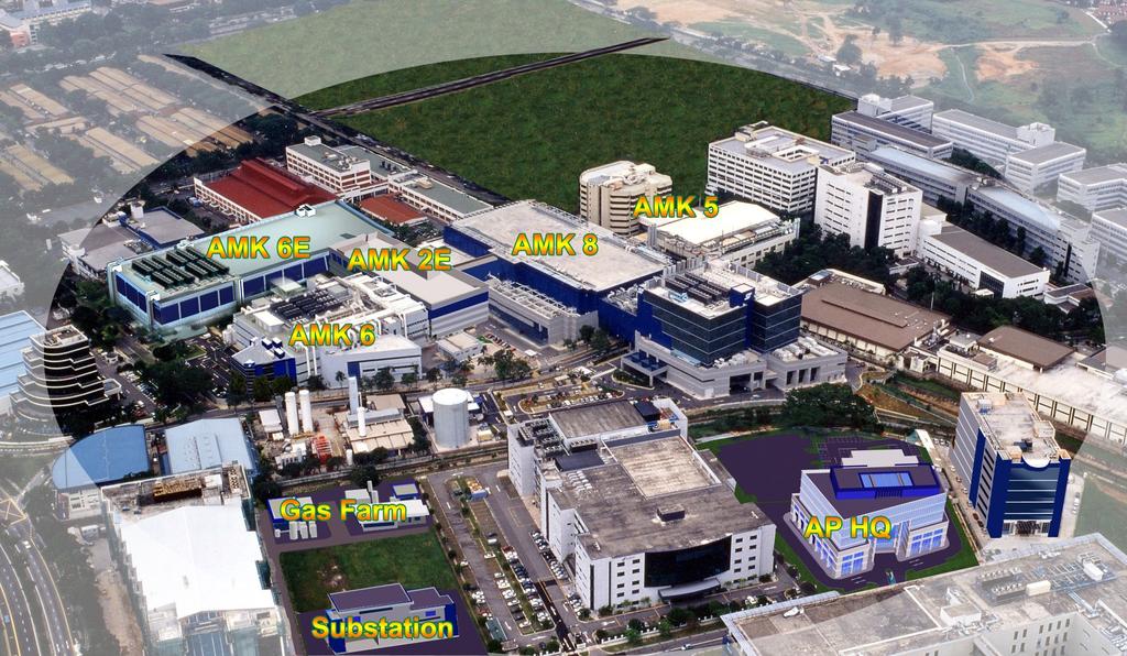
 HIGH LEVEL DIALOGUE ON ASEAN ITALY ECONOMIC RELATIONS Second Edition Shangri-La Hotel, Singapore Wednesday, April 11 and Thursday, April 12, 2018 STMicroelectronics Long-term partnership with Singapore
Continuing Moore s law
 Continuing Moore s law MARK BOHR INTEL SENIOR FELLOW, TECHNOLOGY AND MANUFACTURING GROUP DIRECTOR, PROCESS ARCHITECTURE AND INTEGRATION SEPTEMBER 19, 2017 Legal Disclaimer DISCLOSURES China Tech and Manufacturing
More Course Information
 More Course Information Labs and lectures are both important Labs: cover more on hands-on design/tool/flow issues Lectures: important in terms of basic concepts and fundamentals Do well in labs Do well
Transforming a Leading-Edge Microprocessor Wafer Fab into a World Class Silicon Foundry. Dr. Thomas de Paly
 Transforming a Leading-Edge Microprocessor Wafer Fab into a World Class Silicon Foundry Dr. Thomas de Paly October 06, 2009 Opportunity Meets Vision Vision To be the first truly global semiconductor foundry,
Bringing 3D Integration to Packaging Mainstream
 Bringing 3D Integration to Packaging Mainstream Enabling a Microelectronic World MEPTEC Nov 2012 Choon Lee Technology HQ, Amkor Highlighted TSV in Packaging TSMC reveals plan for 3DIC design based on silicon
Problem 2 If the cost of a 12 inch wafer (actually 300mm) is $3500, what is the cost/die for the circuit in Problem 1.
 is $3500, what is the cost/die for the circuit in Problem 1.") EE 330 Homework 1 Fall 2016 Due Friday Aug 26 Problem 1 Assume a simple circuit requires 1,000 MOS transistors on a die and that all transistors are minimum sized. If the transistors are fabricated in
EE 330 Homework 1 Fall 2016 Due Friday Aug 26 Problem 1 Assume a simple circuit requires 1,000 MOS transistors on a die and that all transistors are minimum sized. If the transistors are fabricated in
Circuits Multi-Projets
 Circuits Multi-Projets 0.35µm, 0.18µm MPW services http://mycmp.fr Grenoble - France Available Processes Process Name Process Feature C35B4C3 0.35µm CMOS 3.3V / 5.0V C35B4C2 0.35µm CMOS 3.3V C35B4O1 C35B4OA
Presenter Name. Larry Morrell Title or job function. Vice President/GM IP Products
 Presenter Name Larry Morrell Title or job function Vice President/GM IP Products AEON Nonvolatile Memory IP Tier 1 customers AEON units shipped 3 6 17 30 11B 1.1B 700M 300M 70M 2005 2006 2007 2008 0.25
envm in Automotive Modules MINATEC Workshop Grenoble, June 21, 2010 May Marco 28, 2009 OLIVO, ST Automotive Group
 envm in Automotive Modules MINATEC Workshop Grenoble, June 21, 2010 May Marco 28, 2009 OLIVO, ST Automotive Group envm in automotive: Outline marketing requirements
emram: From Technology to Applications David Eggleston VP Embedded Memory
 emram: From Technology to Applications David Eggleston VP Embedded Memory 10,000 foot view What are we trying to achieve? 2 Memory is Know Remembering. Think Events 3 Memory is Code Persistence. Data State
Moore s s Law, 40 years and Counting
 Moore s s Law, 40 years and Counting Future Directions of Silicon and Packaging Bill Holt General Manager Technology and Manufacturing Group Intel Corporation InterPACK 05 2005 Heat Transfer Conference
Packaging Innovation for our Application Driven World
 Packaging Innovation for our Application Driven World Rich Rice ASE Group March 14 th, 2018 MEPTEC / IMAPS Luncheon Series 1 What We ll Cover Semiconductor Roadmap Drivers Package Development Thrusts Collaboration
Advanced Packaging For Mobile and Growth Products
 Advanced Packaging For Mobile and Growth Products Steve Anderson, Senior Director Product and Technology Marketing, STATS ChipPAC Growing Needs for Silicon & Package Integration Packaging Trend Implication
Introducing the FX-14 ASIC Design System. Embargoed until November 10, 2015
 Introducing the FX-14 ASIC Design System Embargoed until November 10, 2015 Market Forces Are Driving Need for a New Breed of Semiconductor By 2019: Bandwidth Roughly one million minutes of video will cross
The Foundry-Packaging Partnership. Enabling Future Performance. Jon A. Casey. IBM Systems and Technology Group
 The Foundry-Packaging Partnership Enabling Future Performance Jon A. Casey IBM Fellow IBM Systems and Technology Group 5/30/2013 2012 IBM Corporation Data growth will drive the new IT model Dimensions
3D TECHNOLOGIES: SOME PERSPECTIVES FOR MEMORY INTERCONNECT AND CONTROLLER
 3D TECHNOLOGIES: SOME PERSPECTIVES FOR MEMORY INTERCONNECT AND CONTROLLER CODES+ISSS: Special session on memory controllers Taipei, October 10 th 2011 Denis Dutoit, Fabien Clermidy, Pascal Vivet {denis.dutoit@cea.fr}
Xilinx SSI Technology Concept to Silicon Development Overview
 Xilinx SSI Technology Concept to Silicon Development Overview Shankar Lakka Aug 27 th, 2012 Agenda Economic Drivers and Technical Challenges Xilinx SSI Technology, Power, Performance SSI Development Overview
SOLVING MANUFACTURING CHALLENGES AND BRINGING SPIN TORQUE MRAM TO THE MAINSTREAM
 SEMICON Taipei SOLVING MANUFACTURING CHALLENGES AND BRINGING SPIN TORQUE MRAM TO THE MAINSTREAM Joe O Hare, Marketing Director Sanjeev Aggarwal, Ph.D., VP Manufacturing & Process Everspin Company Highlights
TSBCD025 High Voltage 0.25 mm BCDMOS
 TSBCD025 High Voltage 0.25 mm BCDMOS TSI Semiconductors' 0.25 mm process is a feature rich platform with best in class CMOS, LDMOS, and BiPolar devices. The BCD technology enables logic, Mixed-Signal,
ST Business & Operations
 ST Business & Operations Alain Dutheil Chief Operating Officer A Year-Ago The Global Recession Semiconductor bookings dropped rapidly in Q408; demand remained weak in first half of 2009 Impact on industry
New System Solutions for Laser Printer Applications by Oreste Emanuele Zagano STMicroelectronics
 New System Solutions for Laser Printer Applications by Oreste Emanuele Zagano STMicroelectronics Introduction Recently, the laser printer market has started to move away from custom OEM-designed 1 formatter
Cutting Power Consumption in HDD Electronics. Duncan Furness Senior Product Manager
 Cutting Power Consumption in HDD Electronics Duncan Furness Senior Product Manager Situation Overview The industry continues to drive to lower power solutions Driven by: Need for higher reliability Extended
Opportunities & Challenges: 28nm & 2.5/3-D IC Design and Manufacturing
 Opportunities & Challenges: 28nm & 2.5/3-D IC Design and Manufacturing Vincent Tong Senior Vice President & Asia Pacific Executive Leader Copyright 2011 Xilinx Agenda Xilinx Business Drivers All in at
FBR Capital Markets 12 th Annual Spring Investor Conference
 FBR Capital Markets 12 th Annual Spring Investor Conference ASML continues to execute its leadership strategy Craig De Young VP Investor Relations and Corporate Communications New York City - May 28-29,
Heterogeneous Integration and the Photonics Packaging Roadmap
 Heterogeneous Integration and the Photonics Packaging Roadmap Presented by W. R. Bottoms Packaging Photonics for Speed & Bandwidth The Functions Of A Package Protect the contents from damage Mechanical
OTP & MTP/FRP Non-Volatile Memory IP for Standard Logic CMOS
 OTP & MTP/FRP Non-Volatile Memory IP for Standard Logic CMOS NSCore, Inc. http://www.nscore.com/ Outlines 1. Corporate Overview 2. Program, Read & Erase Mechanism 3. OTP IP Lineups 4. New MTP Technologies
IDEMA Keynote Address February 17, Sanjay Mehrotra COO, Executive VP
 IDEMA Keynote Address February 17, 2005 Sanjay Mehrotra COO, Executive VP The Future of Flash MemoryIs Everywhere Product Line Breadth & Depth USB 2.0 Reader Memory Stick PRO SD TransFlash MP3 Players
Multi-Core Microprocessor Chips: Motivation & Challenges
 Multi-Core Microprocessor Chips: Motivation & Challenges Dileep Bhandarkar, Ph. D. Architect at Large DEG Architecture & Planning Digital Enterprise Group Intel Corporation October 2005 Copyright 2005
TechSearch International, Inc.
 On the Road to 3D ICs: Markets and Solutions E. Jan Vardaman President TechSearch International, Inc. www.techsearchinc.com High future cost of lithography Severe interconnect delay Noted in ITRS roadmap
Credit Suisse European Technology Conference
 Credit Suisse European Technology Conference Franki D Hoore Director European Investor Relations May 12, 2010 / Slide 1 Safe Harbor "Safe Harbor" Statement under the US Private Securities Litigation Reform
Using ASIC circuits. What is ASIC. ASIC examples ASIC types and selection ASIC costs ASIC purchasing Trends in IC technologies
 Using ASIC circuits What is this machine? ASIC examples ASIC types and selection ASIC ASIC purchasing Trends in IC technologies 9.3.2004 Turo Piila 1 9.3.2004 Turo Piila 2 What is ASIC Floorplan and layout
5.2 Technology Leadership
 5.1.3 Unconsolidated Shipments and Gross Sales in 2010 and 2009 Unit: Shipments (8-inch equivalent wafers) / Gross Sales (NT$ thousands) 2010 2009 Shipments Gross Sales Shipments Gross Sales Wafer Package
Versatile RRAM Technology and Applications
 Versatile RRAM Technology and Applications Hagop Nazarian Co-Founder and VP of Engineering, Crossbar Inc. Santa Clara, CA 1 Agenda Overview of RRAM Technology RRAM for Embedded Memory Mass Storage Memory
Toshiba America Electronic Components, Inc. Flash Memory
 Toshiba America Electronic Components, Inc. Flash Memory Fact Sheet Company Overview Combining quality and flexibility with design engineering expertise, TAEC brings a breadth of advanced, next-generation
TSV Test. Marc Loranger Director of Test Technologies Nov 11 th 2009, Seoul Korea
 TSV Test Marc Loranger Director of Test Technologies Nov 11 th 2009, Seoul Korea # Agenda TSV Test Issues Reliability and Burn-in High Frequency Test at Probe (HFTAP) TSV Probing Issues DFT Opportunities
Ultra Fine Pitch RDL Development in Multi-layer ewlb (embedded Wafer Level BGA) Packages
 Packages") Ultra Fine Pitch RDL Development in Multi-layer ewlb (embedded Wafer Level BGA) Packages Won Kyoung Choi*, Duk Ju Na*, Kyaw Oo Aung*, Andy Yong*, Jaesik Lee**, Urmi Ray**, Riko Radojcic**, Bernard Adams***
Ultra Fine Pitch RDL Development in Multi-layer ewlb (embedded Wafer Level BGA) Packages Won Kyoung Choi*, Duk Ju Na*, Kyaw Oo Aung*, Andy Yong*, Jaesik Lee**, Urmi Ray**, Riko Radojcic**, Bernard Adams***
Performance & Reliability Driven Memory solution. MacronixInternational Co., Ltd.
 Performance & Reliability Driven Memory solution MacronixInternational Co., Ltd. About Macronix A Leading Non-Volatile Memory Solutions Provider Founded in 1989 Headquarters Hsin-Chu, Taiwan Total5280
Wafer Probe card solutions
 Wafer Probe card solutions Innovative Solutions to Test Chips in the Semiconductor Industry Our long term experience in the electronic industry and our strong developing and process teams are inspired
L évolution des architectures et des technologies d intégration des circuits intégrés dans les Data centers
 I N S T I T U T D E R E C H E R C H E T E C H N O L O G I Q U E L évolution des architectures et des technologies d intégration des circuits intégrés dans les Data centers 10/04/2017 Les Rendez-vous de
MRAM Developer Day 2018 MRAM Update
 MRAM Developer Day 2018 MRAM Update Barry Hoberman August 2018 1 Disclaimer Observations and opinions >35 years experience in wide variety of memory >12 years experience in MRAM 2012-2017 CEO/Chairman
IoT, Wearable, Networking and Automotive Markets Driving External Memory Innovation Jim Cooke, Sr. Ecosystem Enabling Manager, Embedded Business Unit
 IoT, Wearable, Networking and Automotive Markets Driving External Memory Innovation Jim Cooke, Sr. Ecosystem Enabling Manager, Embedded Business Unit JCooke@Micron.com 2016Micron Technology, Inc. All rights
IC Testing and Development in Semiconductor Area
 IC Testing and Development in Semiconductor Area Prepare by Lee Zhang, 2004 Outline 1. Electronic Industry Development 2. Semiconductor Industry Development 4Electronic Industry Development Electronic
Z-RAM Ultra-Dense Memory for 90nm and Below. Hot Chips David E. Fisch, Anant Singh, Greg Popov Innovative Silicon Inc.
 Z-RAM Ultra-Dense Memory for 90nm and Below Hot Chips 2006 David E. Fisch, Anant Singh, Greg Popov Innovative Silicon Inc. Outline Device Overview Operation Architecture Features Challenges Z-RAM Performance
Applications Emerging to Employ Embedded Non- Volatile Memory
 Applications Emerging to Employ Embedded Non- Volatile Memory May 2011 By: Linh Hong Vice President of Marketing Kilopass Technology Inc. www.kilopass.com To learn more about Kilopass, stop by the Chip
Vertical Circuits. Small Footprint Stacked Die Package and HVM Supply Chain Readiness. November 10, Marc Robinson Vertical Circuits, Inc
 Small Footprint Stacked Die Package and HVM Supply Chain Readiness Marc Robinson Vertical Circuits, Inc November 10, 2011 Vertical Circuits Building Blocks for 3D Interconnects Infrastructure Readiness
Market Update. Peter Jenkins Vice President, Marketing. 24 November 2014
 Market Update Peter Jenkins Vice President, Marketing 24 Forward looking statements This document contains statements relating to certain projections and business trends that are forward-looking, including
Toward a Memory-centric Architecture
 Toward a Memory-centric Architecture Martin Fink EVP & Chief Technology Officer Western Digital Corporation August 8, 2017 1 SAFE HARBOR DISCLAIMERS Forward-Looking Statements This presentation contains
Samsung K9GAG08U0M-PCB0 16 Gbit Multi-Level Cell (MLC) 51 nm Process Technology NAND Flash Memory
 51 nm Process Technology NAND Flash Memory") Samsung K9GAG08U0M-PCB0 16 Gbit Multi-Level Cell (MLC) 51 nm Process Technology NAND Flash Memory Structural Analysis with Additional Layout Feature Analysis For comments, questions, or more information
Samsung K9GAG08U0M-PCB0 16 Gbit Multi-Level Cell (MLC) 51 nm Process Technology NAND Flash Memory Structural Analysis with Additional Layout Feature Analysis For comments, questions, or more information