ANALOG MICROELECTRONICS ( A)
|
|
|
- Carmel Ross
- 6 years ago
- Views:
Transcription
1 ANALOG MICROELECTRONICS ( A) IBM 130 nm CMOS Technology An Introduction to Cadence Virtuoso Layout Tool and the Analog Simulation Environment Prepared By - Azhar A. Chowdhury Updated by Ming Yang CMOS PROCESS Step 1 The first step always is creating the schematic. Then we can perform the layout. Create the schematic of an inverter as per tutorial 1.


2 Figure 1: Schematic of an inverter Step 2: Create the Layout a. In icfb File --> New --> Cell View Tool : Virtuoso Click ok and Layout Editor will open with LSW b. In the layout Editor Options --> Display Set the following parameter: Minor Spacing: 0.01 Major Spacing: 0.1 X Snap Spacing: 0.01 Y Snap Spacing: 0.01 The unit here is in µm, and 0.01µm is the highest precision IBM.13 technology can have.


3 From Display Controls, select 'Pin Names' Display Levels, Start --> 0, Stop --> 20 option --> Layout Editor Set Aperture: You may also want to uncheck the Gravity On box to prevent components snipping together during the layout. c. In the layout editor, you can start the layout. There are two different ways to complete the layout design. Method 1 (traditional approach): In the layout window Create --> Instance (Shortcut i)


4 Place the component in the layout window, Now select the instance and press (Shift + q) for "Edit Instance Properties" Set the length, width, number of fingers according to your design. Select the "Connect S/D/G terminals" *for pmos make sure to select "Add NW contact" Complete the layout similarly, and route the wire accordingly. To put down a wire, select the LSW window and click on the material you would like to use (for example M1 drw means drawing with metal 1), and then use path (W) or rectangular (R) tool to draw. After the layout it should look like this

5 add metal 1 pins to specify input and output nodes 1) select metal1-pn in the LSW window 2) Create -> Pin... 3) give the terminal a name, e.g. VDD 4) select Shape Pin next to Mode (and select rectangle) 5) select Display Pin Name 6) select inputoutput/input/output next to I/O type 7) on the layout, draw a rectangle on the layer to be labelled (metal 1 in this case) and place the text label beside the pin - create four pins in total: VDD, vin, vout and VSS. Method 2 (by layout XL): Layout XL is a function integrated in Cadence that helps the designer to generate all the schematic components (transistors, resistors, pins etc., but except wire) directly from a schematic design. It also tells the designer how to connect components together. Getting familiar with this function can greatly reduce the layout time for a fairly complicated circuit. To invoke Layout XL and generate all components from schematic design: (1) Close your current Virtuoso Layout Editor window (2) In Virtuoso Schematic Editing window, select Tools-->Design Synthesis-->Layout XL (3) Select open existing and locate the file if your layout file has been created before (4) If everything works out correctly, Virtuoso XL Layout Editor window will pop up (5) In this window, select Design-->Gen From Sources (6) Within I/O Pins section, select the material for pins, here we use M1 pn for the layer,
.")


6 then click apply to apply this setup to all pins (7) Click Ok to generate components from schematics Now all the components in your schematic design should be placed into the layout editor, move them into the design area (green box defined by layer prbound). The last step is to route the wire according to the schematic design. When drawing a wire or a rectangular on top of a component, the Layout XL Editor will tell you how it should be connected. For example, when drawing a metal 1 rectangular on the drain of the pfet, the editor will highlight all the places that should be connected together. After the layout it should look similar to the result produced by method 1. The only difference is that the label on top of each pin (in white) does not exist since the pins are automatically generated by the program without any label.

7 Step 3 : Calibre DRC To do a DRC, Layout -> IBM_PDK -> Checking -> Calibre -> DRC Select "Default Runset" from the pop-up. The Environment Variables Setup form will be set at defaults, change: BEOL_STACK = 3_2_3 TECHDIR = /CMC/kits/cmosp13.V DM/IBM_PDK/cmrf8sf/V DM/Calibre/ DENSITY_LOCAL = OFF DESIGN_TYPE = CELL This creates a runset file and opens the Calibre Interactive window. Select a directory below your working directory for the DRC Run Directory (eg. mkdir drc) and then save runset with File - > Save Runset as. The default name of the runset is "ibmpdkdrc.runset1", simply provide the path information. Your working directory is a good place to keep this runset file. The DRC rules, if not automatically filled in, is: /CMC/kits/cmosp13.V DM/IBM_PDK/cmrf8sf/V DM/Calibre/ DRC/cmrf8sf.drc.cal Finally, press the Run DRC button to get your results. After the DRC is complete DRC RVE window will show up with the results. See figure below:

8 If no error then it should look like the figure above. Error will also show up and you can see the reasons for the error. Step 4: Assura LVS To do LVS, Layout -> Assura ->Run LVS Schematic Design Source - DFII Then click Browse on Schematic Design Source to select your schematic from the your library The following Extract Rules, Compare Rules, Binding Files & RSF Include files should be in the form. /CMC/kits/cmosp13.V DM/IBM_PDK/cmrf8sf/V DM/Assura/QRC/32/extract.rul /CMC/kits/cmosp13.V DM/IBM_PDK/cmrf8sf/V DM/Assura/QRC/32/compare.cdl /CMC/kits/cmosp13.V DM/IBM_PDK/cmrf8sf/V DM/Assura/QRC/32/bind.cdl /CMC/kits/cmosp13.V DM/IBM_PDK/cmrf8sf/V DM/Assura/QRC/32/LVSinclude.rsf


9 Click ok to run the LVS and wait until the report appears The following window will appear with all the errors. Click yes If you have any error then the LVS Debug will show all the errors and a description.

10 Step 5: Assura QRC To do QRC, Then, Layout -> Assura ->Run QRC In the Extraction tab Extraction Type - RC Ref Node - /VSS Cap Coupling Mode - Coupling

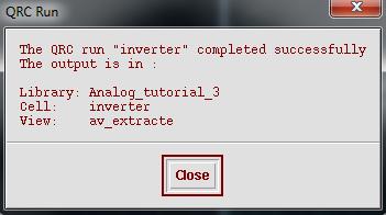
11 In the Setup tab Setup Dir - /CMC/kits/cmosp13.V DM/IBM_PDK/cmrf8sf/V DM/Assura/QRC/32 Output - Extracted View After Successful QRC following window will show up

12 Step 6 - Simulation with the Extracted layout Open the schematics of the circuit test bed. Go to Analog Environment. Setup -> Environment Switch View List -> Write av_extracted before schematic Now you can run your simulation. If you go down in Hierarchy in your test bed circuit, it will take you to extracted view.
UNIVERSITY OF WATERLOO
 UNIVERSITY OF WATERLOO UW ASIC DESIGN TEAM: Cadence Tutorial Description: Part I: Layout & DRC of a CMOS inverter. Part II: Extraction & LVS of a CMOS inverter. Part III: Post-Layout Simulation. The Cadence
Cadence Tutorial 2: Layout, DRC/LVS and Circuit Simulation with Extracted Parasitics
 Cadence Tutorial 2: Layout, DRC/LVS and Circuit Simulation with Extracted Parasitics Introduction This tutorial describes how to generate a mask layout in the Cadence Virtuoso Layout Editor. Use of DIVA
Lab 2. Standard Cell layout.
 Lab 2. Standard Cell layout. The purpose of this lab is to demonstrate CMOS-standard cell design. Use the lab instructions and the cadence manual (http://www.es.lth.se/ugradcourses/cadsys/cadence.html)
TUTORIAL II ECE 555 / 755 Updated on September 11 th 2006 CADENCE LAYOUT AND PARASITIC EXTRACTION
 TUTORIAL II ECE 555 / 755 Updated on September 11 th 2006 CADENCE LAYOUT AND PARASITIC EXTRACTION After finishing a schematic of your design (Tutorial-I), the next step is creating masks which are for
EE434 ASIC & Digital Systems. From Layout to SPICE Simulation (Virtuoso, Calibre, HSpice) Spring 2017 Dae Hyun Kim
 Spring 2017 Dae Hyun Kim") EE434 ASIC & Digital Systems From Layout to SPICE Simulation (Virtuoso, Calibre, HSpice) Spring 2017 Dae Hyun Kim daehyun@eecs.wsu.edu 1 Preparation for Lab2 Download the following file into your working
EE434 ASIC & Digital Systems From Layout to SPICE Simulation (Virtuoso, Calibre, HSpice) Spring 2017 Dae Hyun Kim daehyun@eecs.wsu.edu 1 Preparation for Lab2 Download the following file into your working
Cadence Tutorial. Introduction to Cadence 0.18um, Implementation and Simulation of an inverter. A. Moradi, A. Miled et M. Sawan
 Cadence Tutorial Introduction to Cadence 0.18um, Implementation and Simulation of an inverter A. Moradi, A. Miled et M. Sawan Section 1: Introduction to Cadence You will see how to create a new library
EE115C Digital Electronic Circuits. Tutorial 4: Schematic-driven Layout (Virtuoso XL)
") EE115C Digital Electronic Circuits Tutorial 4: Schematic-driven Layout (Virtuoso XL) This tutorial will demonstrate schematic-driven layout on the example of a 2-input NAND gate. Simple Layout (that won
EE115C Digital Electronic Circuits Tutorial 4: Schematic-driven Layout (Virtuoso XL) This tutorial will demonstrate schematic-driven layout on the example of a 2-input NAND gate. Simple Layout (that won
Amplifier Simulation Tutorial. Design Kit: Cadence 0.18μm CMOS PDK (gpdk180) (Cadence Version 6.1.5)
 (Cadence Version 6.1.5)") Amplifier Simulation Tutorial Design Kit: Cadence 0.18μm CMOS PDK (gpdk180) (Cadence Version 6.1.5) Yongsuk Choi, Marvin Onabajo This tutorial provides a quick introduction to the use of Cadence tools
Amplifier Simulation Tutorial Design Kit: Cadence 0.18μm CMOS PDK (gpdk180) (Cadence Version 6.1.5) Yongsuk Choi, Marvin Onabajo This tutorial provides a quick introduction to the use of Cadence tools
Virtuoso Layout Editor
 This tutorial will cover the basic steps involved in using the Cadence layout editor called Virtuoso, extracting layout, and running simulation on the layout. The inverter layout is used as an example
ECE471/571 Energy Ecient VLSI Design
 ECE471/571 Energy Ecient VLSI Design Project 2 Cadence Setup and Creation of an Inverter Due Date 11:30pm on Friday, January 30 th 2015 Introduction This project will rst walk you through the setup for
Cadence IC Design Manual
 Cadence IC Design Manual For EE5518 ZHENG Huan Qun Lin Long Yang Revised on May 2017 Department of Electrical & Computer Engineering National University of Singapore 1 P age Contents 1 INTRODUCTION...
Setting up the IBM 65nm libraries in Cadence 6.1
 Setting up the IBM 65nm libraries in Cadence 6.1 Preeti Mulage v1 (Jan, 2010) 1. Setting up Cadence 6.1 and Spectre MMSIM 7.1 a. You need to incorporate these lines in order to bring up the latest 6.1
EE 330 Laboratory 3 Layout, DRC, and LVS
 EE 330 Laboratory 3 Layout, DRC, and LVS Spring 2018 Contents Objective:... 2 Part 1 creating a layout... 2 1.1 Run DRC... 2 1.2 Stick Diagram to Physical Layer... 3 1.3 Bulk Connections... 3 1.4 Pins...
ECE471/571 Energy Efficient VLSI Design Project 2 Cadence Setup and Creation of an Inverter Due Date 11:30 am on Friday, February 2 nd, 2018
 ECE471/571 Energy Efficient VLSI Design Project 2 Cadence Setup and Creation of an Inverter Due Date 11:30 am on Friday, February 2 nd, 2018 Introduction This project will first walk you through the setup
EECE 285 VLSI Design. Cadence Tutorial EECE 285 VLSI. By: Kevin Dick Co-author: Jeff Kauppila Co-author: Dr. Arthur Witulski
 Cadence Tutorial EECE 285 VLSI By: Kevin Dick Co-author: Jeff Kauppila Co-author: Dr. Arthur Witulski 1 Table of Contents Purpose of Cadence 1) The Purpose of Cadence pg. 4 Linux 1) The Purpose of Linux
Virtuoso Schematic Composer
 is a schematic design tool from Cadence. In this tutorial you will learn how to put electrical components, make wire connections, insert pins and check for connection error. Start Cadence Custom IC Design
Creating the inv1 cell WITHOUT power pins
 Simulating with extracted parasitic Let s assume I designed the cell inv1, for which I created the views schematic, symbol and layout. Creating the inv1 cell WITHOUT power pins First, create the inverter
EE 330 Laboratory 3 Layout, DRC, and LVS Fall 2015
 EE 330 Laboratory 3 Layout, DRC, and LVS Fall 2015 Contents Objective:... 2 Part 1 Creating a layout... 2 1.1 Run DRC Early and Often... 2 1.2 Create N active and connect the transistors... 3 1.3 Vias...
EE 330 Spring 2018 Laboratory 2: Basic Boolean Circuits
 EE 330 Spring 2018 Laboratory 2: Basic Boolean Circuits Contents Objective:... 2 Part 1: Introduction... 2 Part 2 Simulation of a CMOS Inverter... 3 Part 2.1 Attaching technology information... 3 Part
CS755 CAD TOOL TUTORIAL
 CS755 CAD TOOL TUTORIAL CREATING SCHEMATIC IN CADENCE Shi-Ting Zhou shi-ting@cs.wisc.edu After you have figured out what you want to design, and drafted some pictures and diagrams, it s time to input schematics
CPE/EE 427, CPE 527, VLSI Design I: Tutorial #1, Full Custom VLSI (inverter layout)
") CPE/EE 427, CPE 527, VLSI Design I: Tutorial #1, Full Custom VLSI (inverter layout) Joel Wilder, Aleksandar Milenkovic, ECE Dept., The University of Alabama in Huntsville Adapted from Virginia Tech, Dept.
CPE/EE 427, CPE 527, VLSI Design I: Tutorial #1, Full Custom VLSI (inverter layout) Joel Wilder, Aleksandar Milenkovic, ECE Dept., The University of Alabama in Huntsville Adapted from Virginia Tech, Dept.
VLSI Lab Tutorial 3. Virtuoso Layout Editing Introduction
 VLSI Lab Tutorial 3 Virtuoso Layout Editing Introduction 1.0 Introduction The purpose of this lab tutorial is to guide you through the design process in creating a custom IC layout for your CMOS inverter
Lab 1: An Introduction to Cadence
 GIF-4201/GEL-7016 (Micro-électronique) Lab 1: An Introduction to Cadence Schematic, simulation and layout Gabriel Gagnon-Turcotte, Mehdi Noormohammadi Khiarak and Benoit Gosselin Department of Electrical
Abstract Editor (Last updated: Oct. 23, 2008)
") Abstract Editor (Last updated: Oct. 23, 2008) Abstract Editor Tutorial This tutorial has been created to discuss all of the steps needed to create an abstract Library Exchange Format (LEF) file for custom
Abstract Editor (Last updated: Oct. 23, 2008) Abstract Editor Tutorial This tutorial has been created to discuss all of the steps needed to create an abstract Library Exchange Format (LEF) file for custom
The Procedure for Laying out the inverter in TSMC s 0.35 micron Technogy using MOSIS SCMOS SCN4M_SUBM design rules.
 Page 1 of 5 CADENCE TUTORIAL Creating Layout of an inverter: click on File->library->new a Create Library form appears, fill it as follows: in the name field enter: inverter select "Attach to existing
Design rule illustrations for the AMI C5N process can be found at:
 Cadence Tutorial B: Layout, DRC, Extraction, and LVS Created for the MSU VLSI program by Professor A. Mason and the AMSaC lab group. Revised by C Young & Waqar A Qureshi -FS08 Document Contents Introduction
Cadence Virtuoso Schematic Design and Circuit Simulation Tutorial
 Cadence Virtuoso Schematic Design and Circuit Simulation Tutorial Introduction This tutorial is an introduction to schematic capture and circuit simulation for ENGN1600 using Cadence Virtuoso. These courses
Logging in, starting a shell tool, and starting the Cadence Tool Suite
 EEE 4134 VLSI I Laboratory Lab 0 (Introductory Lab) Logging into Cadence Server, Tool Setup, Cell Library Creation, Introduction to Custom IC Design flow Objectives: To login, start a shell tool and start
FACULTY OF ENGINEERING MULTIMEDIA UNIVERSITY LAB SHEET DIGITAL INTEGRATED CIRCUIT
 FACULTY OF ENGINEERING MULTIMEDIA UNIVERSITY LAB SHEET DIGITAL INTEGRATED CIRCUIT DIC1: Schematic Design Entry, Simulation & Verification DIC2: Schematic Driven Layout Drawing (SDL) Design Rule Check (DRC)
Cadence Tutorial: Schematic Entry and Circuit Simulation of a CMOS Inverter
 Cadence Tutorial: Schematic Entry and Circuit Simulation of a CMOS Inverter Introduction This tutorial describes the steps involved in the design and simulation of a CMOS inverter using the Cadence Virtuoso
AMS 0.18 µm PDK Setup and Cadence Tutorial Contributors
 AMS 0.18 µm PDK Setup and Cadence Tutorial Contributors Muhammad Ahmed, Sita Asar, and Ayman Fayed, Power Management Research Lab, https://pmrl.osu.edu, Department of Electrical and Computer Engineering,
Cadence Schematic Tutorial. EEE5320/EEE4306 Fall 2015 University of Florida ECE
 Cadence Schematic Tutorial EEE5320/EEE4306 Fall 2015 University of Florida ECE 1 Remote access You may access the Linux server directly from the NEB Computer Lab using your GatorLink username and password.
VLSI Lab Tutorial 1. Cadence Virtuoso Schematic Composer Introduction
 VLSI Lab Tutorial 1 Cadence Virtuoso Schematic Composer Introduction 1.0 Introduction The purpose of the first lab tutorial is to help you become familiar with the schematic editor, Virtuoso Schematic
Layout and Layout Verification. of an Inverter Circuit
 Layout and Layout Verification of an Inverter Circuit Santa Clara University Department of Electrical Engineering By Piyush Panwar Under Guidance of Dr Samiha Mourad Date of Last Revision: August 7, 2010
ELEC451 Integrated Circuit Engineering Using Cadence's Virtuoso Layout Editing Tool
 ELEC451 Integrated Circuit Engineering Using Cadence's Virtuoso Layout Editing Tool Contents Contents 1. General 2. Creating and Working On a Layout o 2.1 Undoing/Re-doing an Action o 2.2 Display Options
Fall 2008: EE5323 VLSI Design I using Cadence
 1 of 23 9/17/2008 6:47 PM Fall 2008: EE5323 VLSI Design I using Cadence This tutorial has been adapted from EE5323 offered in Fall 2007. Thanks to Jie Gu, Prof. Chris Kim and Satish Sivaswamy of the University
DOWNLOAD PDF CADENCE WAVEFORM CALCULATOR USER GUIDE
 Chapter 1 : CSE / Cadence Tutorial The Cadence Design Communities support Cadence users and technologists interacting to exchange ideas, news, technical information, and best practices to solve problems
DRC and LVS checks using Cadence Virtuoso Version 3.0
 DRC and LVS checks using Cadence Virtuoso Version 3.0 Start virtuoso l l Open a virtuoso session in the directory which contains the required cds.lib and lib.def files. Command : virtuoso & Open the layout
ESE570 Spring University of Pennsylvania Department of Electrical and System Engineering Digital Integrated Cicruits AND VLSI Fundamentals
 University of Pennsylvania Department of Electrical and System Engineering Digital Integrated Cicruits AND VLSI Fundamentals ESE570, Spring 2019 HW5: Delay and Layout Sunday, February 17th Due: Friday,
EECS 627, Lab Assignment 3
 EECS 627, Lab Assignment 3 1 Introduction In this lab assignment, we will use Cadence ICFB and Calibre to become familiar with the process of DRC/LVS checks on a design. So far, we have placed and routed
This is a brief tutorial about building a Symbol for a Schematic in Cadence IC design tool environment for hierarchical design of schematics.
 This is a brief tutorial about building a Symbol for a Schematic in Cadence IC design tool environment for hierarchical design of schematics. 1. > cd work035 2. > cadsetup ams035 3. > virtuoso& IMPORTANT:
ECE425: Introduction to VLSI System Design Machine Problem 3 Due: 11:59pm Friday, Dec. 15 th 2017
 ECE425: Introduction to VLSI System Design Machine Problem 3 Due: 11:59pm Friday, Dec. 15 th 2017 In this MP, you will use automated tools to synthesize the controller module from your MP2 project into
Process technology and introduction to physical
 Neuromorphic Engineering II Lab 3, Spring 2014 1 Lab 3 March 10, 2014 Process technology and introduction to physical layout Today you will start to learn to use the Virtuoso layout editor XL which is
EDA-BASED DESIGN PRACTICAL LABORATORY SESSION No. 3
 LABORATOIRE DE SYSTEMES MICROELECTRONIQUES EPFL STI IMM LSM ELD Station nº 11 CH-1015 Lausanne Téléphone : Fax : E-mail : Site web : +4121 693 6955 +4121 693 6959 lsm@epfl.ch lsm.epfl.ch EDA-BASED DESIGN
Cadence Tutorial A: Schematic Entry and Functional Simulation Created for the MSU VLSI program by Andrew Mason and the AMSaC lab group.
 Cadence Tutorial A: Schematic Entry and Functional Simulation Created for the MSU VLSI program by Andrew Mason and the AMSaC lab group. Revision Notes: Aug. 2003 update and edit A. Mason add intro/revision/contents
CMOS Design Lab Manual
 CMOS Design Lab Manual Developed By University Program Team CoreEl Technologies (I) Pvt. Ltd. 1 Objective Objective of this lab is to learn the Mentor Graphics HEP2 tools as well learn the flow of the
DRC and LVS checks using Cadence Virtuoso Version 2.0
 DRC and LVS checks using Cadence Virtuoso Version 2.0 Start virtuoso l l Open a virtuoso session in the directory which contains the required cds.lib and lib.def files. Command : virtuoso & Open the layout
EE 330 Laboratory Experiment Number 11
 EE 330 Laboratory Experiment Number 11 Design and Simulation of Digital Circuits using Hardware Description Languages Fall 2017 Contents Purpose:... 3 Background... 3 Part 1: Inverter... 4 1.1 Simulating
Professor Muller Fall 2016 Sameet Ramakrishnan Eric Chang Adapted from prior EE140 and EE141 labs. EE 140/240A Lab 0 Full IC Design Flow
 Professor Muller Fall 2016 Sameet Ramakrishnan Eric Chang Adapted from prior EE140 and EE141 labs EE 140/240A Lab 0 Full IC Design Flow In this lab, you will walk through the full process an analog designer
EEC 116 Fall 2011 Lab #1 Cadence Schematic Capture and Layout Tutorial
 EEC 116 Fall 2011 Lab #1 Cadence Schematic Capture and Layout Tutorial Dept. of Electrical and Computer Engineering University of California, Davis September 26, 2011 Reading: Rabaey Chapters 1, 2, A,
CMOS INVERTER LAYOUT TUTORIAL
 PRINCESS SUMAYA UNIVERSITY FOR TECHNOLOGY CMOS INVERTER LAYOUT TUTORIAL We will start the inverter by drawing a PMOS. The first step is to draw a poly layer. Click on draw a rectangle and choose the poly
ESE 570 Cadence Lab Assignment 2: Introduction to Spectre, Manual Layout Drawing and Post Layout Simulation (PLS)
") ESE 570 Cadence Lab Assignment 2: Introduction to Spectre, Manual Layout Drawing and Post Layout Simulation (PLS) Objective Part A: To become acquainted with Spectre (or HSpice) by simulating an inverter,
ESE 570 Cadence Lab Assignment 2: Introduction to Spectre, Manual Layout Drawing and Post Layout Simulation (PLS) Objective Part A: To become acquainted with Spectre (or HSpice) by simulating an inverter,
Prepared by Dr. Ulkuhan Guler GT-Bionics Lab Georgia Institute of Technology
 Prepared by Dr. Ulkuhan Guler GT-Bionics Lab Georgia Institute of Technology OUTLINE Introduction Mapping for Schematic and Layout Connectivity Generate Layout from Schematic Connectivity Some Useful Features
EE5323/5324 VLSI Design I/II using Cadence
 1 of 18 2009-1-23 23:58 Spring 2009: EE5323/5324 VLSI Design I/II using Cadence This tutorial has been adapted from EE5323 offered in Fall 2007. Thanks to Jie Gu, Prof. Chris Kim and Satish Sivaswamy of
Analog IC Schematic Capture. Mentor Graphics 2006
 Analog IC Schematic Capture Mentor Graphics 2006 Santa Clara University Department of Electrical Engineering Date of Last Revision: February 6, 2007 Table of Contents 1. Objective...3 2. Setup & Preparation...4
Introduction to Design Architect
 SANTA CLARA UNIVERSITY Dept. of Electrical Engineering Mentor Graphics Tutorials Introduction to Design Architect Yiching Chen Sangeetha Raman S. Krishnan I. Introduction II. This document contains a step-by-step
Microelectronica. Full-Custom Design with Cadence Tutorial
 Área Científica de Electrónica Microelectronica Full-Custom Design with Cadence Tutorial AustriaMicroSystems C35B3 (HIT-Kit 3.70) Marcelino Santos Table of contends 1. Starting Cadence... 3 Starting Cadence
Revision Notes: July2004 Generate tutorial for single transistor analysis. Based on existing schematic entry tutorial developed for ECE410
 Cadence Analog Tutorial 1: Schematic Entry and Transistor Characterization Created for the MSU VLSI program by Professor A. Mason and the AMSaC lab group. Revision Notes: July2004 Generate tutorial for
Select the technology library: NCSU_TechLib_ami06, then press OK.
 ECE 126 Inverter Tutorial: Schematic & Symbol Creation Created for GWU by Anis Nurashikin Nordin & Thomas Farmer Tutorial adapted from: http://www.ee.ttu.edu/ee/cadence/commondirectory/final%20tutorials/digitalcircuitsimulationusingvirtuoso.doc
EE115C Digital Electronic Circuits. Tutorial 2: Hierarchical Schematic and Simulation
 EE115C Digital Electronic Circuits Tutorial 2: Hierarchical Schematic and Simulation The objectives are to become familiar with Virtuoso schematic editor, learn how to create the symbol view of basic primitives,
CPE/EE 427, CPE 527, VLSI Design I: Tutorial #2, Schematic Capture, DC Analysis, Transient Analysis (Inverter, NAND2)
") CPE/EE 427, CPE 527, VLSI Design I: Tutorial #2, Schematic Capture, DC Analysis, Transient Analysis (Inverter, NAND2) Joel Wilder, Aleksandar Milenkovic, ECE Dept., The University of Alabama in Huntsville
CPE/EE 427, CPE 527, VLSI Design I: Tutorial #2, Schematic Capture, DC Analysis, Transient Analysis (Inverter, NAND2) Joel Wilder, Aleksandar Milenkovic, ECE Dept., The University of Alabama in Huntsville
CADENCE SETUP. ECE4430-Analog IC Design
 CADENCE SETUP This short tutorial shows how to configure Cadence to use the NCSU Cadence Design Kit (CDK) with access to the ON Semiconductor C5 0.5-µm and the TSMC 0.35-µm CMOS processes libraries. In
Full Custom Integrated Circuit (IC) Design Flow at U.S. Army Research Laboratory
 Design Flow at U.S. Army Research Laboratory") Full Custom Integrated Circuit (IC) Design Flow at U.S. Army Research Laboratory by James Wilson ARL-TN-0422 February 2011 Approved for public release; distribution unlimited. NOTICES Disclaimers The findings
Full Custom Integrated Circuit (IC) Design Flow at U.S. Army Research Laboratory by James Wilson ARL-TN-0422 February 2011 Approved for public release; distribution unlimited. NOTICES Disclaimers The findings
Verifying the Multiplexer Layout
 4 This chapter introduces you to interactive verification. You will perform two different tests in the Virtuoso layout editor while using Assura interactive verification products. One test uses the Design
Mentor Graphics VLSI CAD Tutorials
 VLSI Design Flow Using Mentor-Graphics Tools Mentor Graphics VLSI CAD Tutorials School of Engineering Santa Clara University Santa Clara, CA 95053 At the Design Center, School of Engineering, of Santa
EE 140/240A - Full IC Design Flow Tutorial
 Original document by Filip Maksimovic & Mike Lorek, Spring 2015, derived from earlier EE141 lab manuals Revisions for IC6 by David Burnett & Thaibao Phan, Spring 2016 Revisions made by Nandish Mehta to
More information can be found in the Cadence manuals Virtuoso Layout Editor User Guide and Cadence Hierarchy Editor User Guide.
 Chapter 6 Building with Layout This chapter consists of two parts. The first describes the generation of layout views and the second deals with the various tools used for verifying the layout, both physical
Guide to the CSE 577 Lab and Cad tools
 Guide to the CSE 577 Lab and Cad tools 1. Introduction The objective of this tutorial is to give you an overview to (1) setup the Cadence and Synopsys hspice tools for your account in IST 218 Lab, (2)
A Tutorial on Using the Cadence Virtuoso Editor to create a CMOS Inverter with CMOSIS5 Technology
 A Tutorial on Using the Cadence Virtuoso Editor to create a CMOS Inverter with CMOSIS Technology Developed by Ted Obuchowicz VLSI/CAD Specialist, Dept. of Electrical and Computer Engineering Concordia
Cadence Tutorial A: Schematic Entry and Functional Simulation Created for the MSU VLSI program by Professor A. Mason and the AMSaC lab group.
 Cadence Tutorial A: Schematic Entry and Functional Simulation Created for the MSU VLSI program by Professor A. Mason and the AMSaC lab group. Revision Notes: Jan. 2006 Updated for use with spectre simulator
Tutorial II: Cadence Virtuoso ECE6133: Physical Design Automation of VLSI Systems Georgia Institute of Technology Prof.
 Tutorial II: Cadence Virtuoso ECE6133: Physical Design Automation of VLSI Systems Georgia Institute of Technology Prof. Sung Kyu Lim I. Setup for Cadence Virtuoso 1. Copy the following files into your
EE4111 Advanced Analog Electronics Design. Spring 2009 Experiment #4 April 6 ~ April 17
 EE4111 Advanced Analog Electronics Design Spring 2009 Experiment #4 April 6 ~ April 17 Setup Cadence in VLSI Lab 1) Copy files $ cp r /home/grads/ee4111ta ~/ 2) Edit your.cshrc file -- Include the following
Cadence Tutorial D: Using Design Variables and Parametric Analysis Document Contents Introduction Using Design Variables Apply Apply
 Cadence Tutorial D: Using Design Variables and Parametric Analysis Created for the MSU VLSI program by Casey Wallace Last Updated by: Patrick O Hara SS15 Document Contents Introduction Using Design Variables
EE 330 Laboratory Experiment Number 11 Design and Simulation of Digital Circuits using Hardware Description Languages
 EE 330 Laboratory Experiment Number 11 Design and Simulation of Digital Circuits using Hardware Description Languages Fall 2015 Purpose: The purpose of this experiment is to develop methods for using Hardware
The original document link is
 Tutorial:Analog Artist with HSPICE The original document link is http://www.eda.ncsu.edu/wiki/tutorial:analog_artist_with_hspice This tutorial will introduce you to the Cadence Environment: specifically
UNIVERSITY OF CALIFORNIA College of Engineering Department of Electrical Engineering and Computer Sciences Lab #2: Layout and Simulation
 UNIVERSITY OF CALIFORNIA College of Engineering Department of Electrical Engineering and Computer Sciences Lab #2: Layout and Simulation NTU IC541CA 1 Assumed Knowledge This lab assumes use of the Electric
Introduction to laboratory exercises in Digital IC Design.
 Introduction to laboratory exercises in Digital IC Design. A digital ASIC typically consists of four parts: Controller, datapath, memory, and I/O. The digital ASIC below, which is an FFT/IFFT co-processor,
An overview of standard cell based digital VLSI design
 An overview of standard cell based digital VLSI design Implementation of the first generation AsAP processor Zhiyi Yu and Tinoosh Mohsenin VCL Laboratory UC Davis Outline Overview of standard cellbased
CMOS VLSI Design Lab 4: Full Chip Assembly
 CMOS VLSI Design Lab 4: Full Chip Assembly In this final lab, you will assemble and simulate your entire MIPS microprocessor! You will build your top level chip cell by connecting the datapath, aludec,
The following is a procedure for extracting a layout, doing a layout vs. schematic check, and then simulating the extracted layout with Cadence.
 The following is a procedure for extracting a layout, doing a layout vs. schematic check, and then simulating the extracted layout with Cadence. (This might not be the best way, but it works!) 1) Realize
Creating LEF File. Abstract Generation: Creating LEF Tutorial File Release Date: 01/13/2004. Export GDS:
 Creating LEF Tutorial 1-1 - Creating LEF File Abstract Generation: Export GDS: Abstract generator comes as a part of the Silicon Ensemble package. As such, it cannot directly read ICFB library databases.
Laboratory 6. - Using Encounter for Automatic Place and Route. By Mulong Li, 2013
 CME 342 (VLSI Circuit Design) Laboratory 6 - Using Encounter for Automatic Place and Route By Mulong Li, 2013 Reference: Digital VLSI Chip Design with Cadence and Synopsys CAD Tools, Erik Brunvand Background
EE 330 Laboratory Experiment Number 11 Design, Simulation and Layout of Digital Circuits using Hardware Description Languages
 EE 330 Laboratory Experiment Number 11 Design, Simulation and Layout of Digital Circuits using Hardware Description Languages Purpose: The purpose of this experiment is to develop methods for using Hardware
Lab 1: Cadence Custom IC design tools- Setup, Schematic capture and simulation
 Lab 1: Cadence Custom IC design tools- Setup, Schematic capture and simulation Brittany Duffy EE 330- Integrated Electronics Lab Section B Professor Randy Geiger 1/24/13 Introduction The main goal of this
Lab 4 LVS and Post layout Simulation
 Lab 4 LVS and Post layout Simulation Objective: In this lab you will learn 1. How to check if your layout that you drew in lab 3 matches your schematic that you drew in lab 2. 2. How to do the post layout
Synthesis and APR Tools Tutorial
 Synthesis and APR Tools Tutorial (Last updated: Oct. 26, 2008) Introduction This tutorial will get you familiarized with the design flow of synthesizing and place and routing a Verilog module. All the
Laboratory 3. EE 342 (VLSI Circuit Design) - Using Spectre netlist and Calculator for simulation
 - Using Spectre netlist and Calculator for simulation") EE 342 (VLSI Circuit Design) Laboratory 3 - Using Spectre netlist and Calculator for simulation By Mulong Li, 2013 1 Background knowledge Spectre: is a SPICE-class circuit simulator. It provides the basic
EE 342 (VLSI Circuit Design) Laboratory 3 - Using Spectre netlist and Calculator for simulation By Mulong Li, 2013 1 Background knowledge Spectre: is a SPICE-class circuit simulator. It provides the basic
DC Circuit Simulation
 Chapter 2 DC Circuit Simulation 2.1 Starting the Project Manager 1. Select Project Manager from the Start All Program Cadence Release 16.5 Project Manager. 2. Select Allegro PCB Designer (Schematic) from
Basic Analog Simulation in Cadence
 York University Department of Electrical Engineering and Computer Science EMIL Tutorial Series Tutorial #1 Basic Analog Simulation in Cadence In this tutorial we step through how to start Cadence (or at
Chip Core. Final Assembly. Core Sizes. Connecting Core to Pads. Core. Pad Ring The connection to the outside world
 Final Assembly Your final project chip consists of a core and a pad ring Core is the guts Pad ring (or pad frame) connects the guts to the outside world It s critical to do a functional simulation of your
Extraction of Parasitic Capacitance and Resistances for HSPICE Simulation
 Extraction of Parasitic Capacitance and Resistances for HSPICE Simulation Make the layout window active and select Calibre > Run PEX from the top menu bar to start a Parasitic EXtraction. You will need
CS/EE 5720/6720 Analog IC Design Tutorial for Schematic Design and Analysis using Spectre
 CS/EE 5720/6720 Analog IC Design Tutorial for Schematic Design and Analysis using Spectre Introduction to Cadence EDA: The Cadence toolset is a complete microchip EDA (Electronic Design Automation) system,
HOMEWORK 9 CMPEN 411 Due: 4/12/ :30pm
 HOMEWORK 9 CMPEN 411 Due: 4/12/2016 11:30pm Learning Objective Complete the full 8 bit RISC microprocessor chip design by placing the processor core design into the 40 pin 'tiny' chip pad frame. Do verify
Final Assembly. Chip Core
 Final Assembly Your final project chip consists of a core and a pad ring Core is the guts Pad ring (or pad frame) connects the guts to the outside world It s critical to do a functional simulation of your
Creating Verilog Tutorial Netlist Release Date: 01/13/2005(Version 2)
") Creating Verilog Tutorial 2-1 - Creating a verilog netlist for a schematic: The verilog netlist is necessary for automatic layout (placement and routing) tools. It contains information about the I/O pins
Creating Verilog Tutorial 2-1 - Creating a verilog netlist for a schematic: The verilog netlist is necessary for automatic layout (placement and routing) tools. It contains information about the I/O pins
INTRODUCTION TO MENTOR GRAPHICS DESIGN TOOLS
 INTRODUCTION TO MENTOR GRAPHICS DESIGN TOOLS 1. RUNNING MENTOR GRAPHICS Erdem S. Erdogan 09.13.2006 Note: These commands can be run remotely via ssh to one of the DSIL machines. If running remotely, ignore
EE 330 Spring Laboratory 2: Basic Boolean Circuits
 EE 330 Spring 2013 Laboratory 2: Basic Boolean Circuits Objective: The objective of this experiment is to investigate methods for evaluating the performance of Boolean circuits. Emphasis will be placed
HOMEWORK 10 CMPEN 411 Due: 4/28/ :30pm
 HOMEWORK 10 CMPEN 411 Due: 4/28/2016 11:30pm Instruction First, fabrication ready the full 8 bit RISC microprocessor chip: redesign the chip (its components) to fit the entire chip fitted into the 40 pin
Lab. Course Goals. Topics. What is VLSI design? What is an integrated circuit? VLSI Design Cycle. VLSI Design Automation
 Course Goals Lab Understand key components in VLSI designs Become familiar with design tools (Cadence) Understand design flows Understand behavioral, structural, and physical specifications Be able to
Simulation with Verilog-XL
 Simulation with Verilog-XL Adapted from Princeton Cadence Page (http://www.ee.princeton.edu/~cadence/usr/verilog.html) Until now, we have been using the Analog Environment to do simulations. This simulator