PDK-Based Analog/Mixed-Signal/RF Design Flow 11/17/05
|
|
|
- Hugh Tate
- 6 years ago
- Views:
Transcription

1 PDK-Based Analog/Mixed-Signal/RF Design Flow 11/17/05
2 Silvaco s What is a PDK? Which people build, use, and support PDKs? How do analog/mixed-signal/rf engineers use a PDK to design ICs? What is an analog/mixed-signal/rf design flow? How do you build a good PDK? How to you measure quality of PDK? What is the FSA PDK Checklist? How do you support designers using a PDK? - 2 -
3 What is a PDK? A process design kit (PDK) is a collection of verified data files that are used by a set of custom IC design EDA tools to provide a complete analog/mixed-signal/rf design flow. These data files include schematic symbols, SPICE models, Parameterized Cells (PCELLS), DRC/LVS runsets, parasitic extraction runsets, and scripts that run by the EDA tools to automate the generation and verification of design data
4 Who are the People Who Build and Use PDKs? Foundries Manufacture Silicon Wafers Build PDKs for their customers Electronic Design Automation Vendors Make Software Tools Build PDKs for their customers Fabless Semiconductor Companies Make Integrated Circuits Use PDKs to Design ICs Integrated Device Manufactures (IDM) Manufacture and Design ICs, build and use PDKs ASIC Vendors Design ICs for System Designers, build and use PDKs System Designers Manufacture Cell Phones and other products - 4 -
5 Why Adopt PDK Design Methodology? Jump-starts designers with an instantly productive environment for new design projects DESIGN PRODUCTIVITY Ensure manufacturing success with pre-configured schematic symbols and layout technology files DESIGN QUALITY Tightly links EDA tools, IC designers, and foundry support for fast time-to-market TAT Reduces costly rework cycles PROFITABILITY Rapidly becoming industry standard for analog circuit design methodology - 5 -


6 PDKs Enable an Integrated Analog/Mixed-Signal/RF Design Tool Flow ß At top left is a bandgap circuit captured with Schematic Capture using symbols from the PDK ß Pcells are instantiated by Layout Editor with flight lines ß Cells are placed and wired to make final layout ß SPICE simulates extracted bandgap over temperature -6-

7 Front-end Analog/Mixed-Signal/RF Design Flow Front-End Solution EDA Tools: Schematic, Simulation Control, Multi-Level Circuit Simulation, Waveform Viewing Supported By: Symbol libraries, SPICE Models, Callbacks - 7 -
 -")
8 Back-end Analog/Mixed-Signal/RF Design Flow Back-End Solution EDA Tools: Layout Editor, DRC, LVS, Parasitic Extraction Supported by: Tech files, Rule decks, Parameterized Cells (Pcells) - 8 -

9 Complete PDK-Based Analog/Mixed-Signal/RF Design Flow - 9 -

10 Silvaco PDK-Based Analog/Mixed-Signal/RF Design Flow


11 Gateway Schematic Editor and Analog/Mixed- Signal/RF Front-End Front-end to hierarchical design with cross-probing, marching waveforms, analysis options, and optimization. Mixes transistor and behavioral level (Verilog-A) schematics


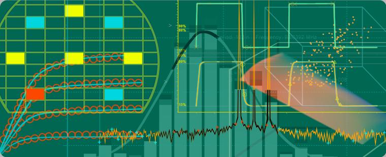
12 SmartSpice Circuit Simulator with SmartView Transient noise simulation with voltage and noise waveforms at 2 different circuit nodes. SmartSpice-64 simulates full chip power and signal integrity of extracted clock trees SmartView produces annotated plots and graphs of measurements of time, voltage, current, and power for rise time, slope, vector calculator, and eye diagrams


13 Expert Layout Editor Generates Parameterized Cells High capacity loads over 10 gigabytes in minutes with fast panning and zooming Fully customizable hotkeys, macros, toolbars, layers, colors, and stipples can be directly imported All-angle polygons for analog


14 Guardian DRC/LPE/LVS Verification Intuitive graphical DRC error debugging in Expert Interactive hierarchical crossprobing of LVS discrepancy Net Tracing follows nets and devices between layout and schematic


15 HIPEX Full-Chip Parasitic Extractor Product Design Flow HIPEX-C provides detailed coupling capacitor netlists for accurate analyses of overlap, lateral, and fringe capacitances HIPEX-RC supports SPICE, DSPF formats
16 How do you Build a Good PDK? Silvaco process design kit (PDK) development services jump-starts analog and mixed-signal design teams and the CAD teams who support them with all of the foundryspecific models, symbols, rule decks and parameterized cells (P-cells) required for rapid, sustainable success using the complete Silvaco custom IC design toolset Build it yourself using the following steps: Write a specification Collect the foundry documents Build a front-end kit Build a back-end kit Verify the kit Package the kit for distribution Support the kit as process technology or EDA tools change
17 Foundry Design Documents for PDK Development Basic Level - Standard Foundry Documents HSPICE Model Layout Design Rules DRC/LVS technology file Compatibility Level - standard PDK Kit for: GDSII examples with layer map Schematic symbol standard Documentation from other PDKs FSA Checklist PDK Development Accelerators Script files from other PDKs DRC/LVS testcase suite
18 PDK Front-end Deliverables Schematic Symbols for the Gateway Schematic Editor invokes parameterized cells in the Expert Layout design tool that are DRC and LVS correct These parameterized symbols and respective subcircuits are integrated and tested with the SPICE models to assure a standard convention for transistor level simulation P-cells are written in the LISA Scripting Language. SPICE Models SPICE model files verified with the SmartSpice Circuit Simulator at the foundry supplied process corners (temperature, voltage, process) Silvaco can optionally extract a set of models from a wafer or measured data to produce a complete measured vs. simulation for each device
19 PDK Back-end Deliverables Technology Files layer files that correlate the legal GDSII layers for each of the process layers for layout and verification tools Display files to customize the layout and schematic tools for GDS layers, display colors and user-customizable hot keys Rule Decks contain the layout rules encoded into the format used by: Expert Layout Editor Guardian DRC /LVS/LPE tools HIPEX Full-chip Parasitic Extractor Parameterized Cells enable annotated device schematics to be automatically drawn in the Expert Layout Editor, DRC and LVS correct, using the LISA scripting language
20 Silvaco PDK Development Services Process Flow Step Foundry Silvaco Deliver Foundry Data P Extract SPICE Models Deliver Front-End Kit (schematic symbols with SPICE models) P Deliver Back-end Kit (DRC, LVS, LPE, Pcells) P Design Review and Training optional P Validate PDK optional P Deliver Final PDK P optional Support Mutual Customers optional P
21 Migrating Other Design Flows to Build Silvaco PDK Data Format of Design Tool Schematics Layout Editor Tech Files Layout Data DRC/LVS Decks SPICE models SPICE netlists, commands Silvaco Compatibility EDIF Import in Gateway Expert reads Virtuoso files Expert reads/writes GDSII Guardian translates Calibre and Diva/Dracula/Assura SmartSpice reads HSPICE SmartSpice reads HSPICE

22 How to you measure quality of PDK? Other Industries Have the Same Problems 1924 Federal Food and Drug Act prohibits untrue claims 1973 Required on all foods with added nutrients or claims 1989 New Rules 1993 Label Finalized months later appears on all food packages
23 PDK Checklist Foundry Process Documents Foundry Process Documents Document Document Number & Title Section Revision Date Design Manual (Devices) Electrical Parameters Design Layout Rules Spice Model RF Parameters/Modeling Noise Model Matching Models ESD Guidelines DRC LVS Parasitic Extraction Layer Map
24 PDK Checklist EDA Tool Support EDA Tools Supported and Verified for Use with this PDK Type Vendor and Tool Version Version Date Schematic Simulation Control Circuit Simulator (A) Circuit Simulator (B) Circuit Simulator (C) Circuit Simulator (D) Layout Editor DRC Checker LVS Checker Parasitic Extractor Analysis Tools
25 PDK Checklist Devices in Device Table Device Types Supported by MS/RF Processes Device Type Examples of Devices of this Type MOS NMOS/PMOS LV/HV, LVth/HVth, thick oxide, or floating gate BJT NPN/PNP, LV/HV, lateral, vertical Diodes N+/PW, P+/NW, Zener Capacitors poly-poly, MIM, tunnel, hi-q Resistors n-diff, p-diff, n-well, poly0, poly1, polyn, fuse, and metal Inductors standard and differential Varactors MOS, junction, and hyperabrupt
26 PDK Checklist Device Table
27 PDK Quality Criteria Accuracy, Clarity, Integration Enable Accurate Time Domain Analysis Accurate Passive Characterization of RC Accurate Analog/RF Models High Frequency Noise Low Frequency Noise - Flicker Subckt Macro Models RLC Passives Pcell Integrated Design Flow Layout Editors and Pcells that can draw spiral Inductors Extraction and Signal Integrity Analysis
28 Current Silvaco Foundry Partners
29 Silvaco PDK Delivery Status Delivered 0.5u High Voltage 40V BCD/BiCMOS 0.6u Mixed Signal 60V CMOS 0.6u Mixed Signal 40V CMOS 0.6u Mixed Signal 12V CMOS 0.6u Mixed Signal CMOS 0.18u RF CMOS 1.25u Bipolar MOSIS SCMOS In Development 0.5u Mixed Signal CMOS 0.18u SiGe 1.5u 80V BCD 0.13u RF CMOS
30 Summary: Silvaco PDK-Based Analog Design Flow Single-Vendor Front-to-Back Solution Schematic entry front-end with complete set of circuit and mixedmode simulators Layout back-end with DRC/LVS/LPE and parasitic extraction PDKs create integrated analog design tool flow Easy Migration Path for Legacy Designs Industry-standard EDA formats and translator support Foundries Support for Rapid Silvaco PDK Development PDK tightly links EDA tools, IC designers and foundries for optimal manufacturing success Time-to-market for analog in CMOS Affordable and Flexible Licensing Highest value, lowest risk, and best support
Expert Layout Editor. Technical Description
 Expert Layout Editor Technical Description Agenda Expert Layout Editor Overview General Layout Editing Features Technology File Setup Multi-user Project Library Setup Advanced Programmable Features Schematic
Guardian NET Layout Netlist Extractor
 Outline What is Guardian NET Key Features Running Extraction Setup Panel Layout Annotation Layout Text Extraction Node Naming Electric Rule Checking (ERC) Layout Hierarchy Definition Hierarchy Checker
Harmony-AMS Analog/Mixed-Signal Simulator
 Harmony-AMS Analog/Mixed-Signal Simulator Yokohama, June 2004 Workshop 7/15/04 Challenges for a True Single-Kernel A/MS Simulator Accurate partition of analog and digital circuit blocks Simple communication
HIPEX Full-Chip Parasitic Extraction. Summer 2004 Status
 HIPEX Full-Chip Parasitic Extraction Summer 2004 Status What is HIPEX? HIPEX Full-Chip Parasitic Extraction products perform 3D-accurate and 2D-fast extraction of parasitic capacitors and resistors from
Hipex Full-Chip Parasitic Extraction
 What is Hipex? products perform 3D-accurate and 2D-fast extraction of parasitic capacitors and resistors from hierarchical layouts into hierarchical transistor-level netlists using nanometer process technology
Detailed Presentation
 Detailed Presentation PDK Leadership - Developing and Delivering High Quality PDKs Simucad PDKs are being rapidly adopted worldwide by leading foundries and design houses because of their quality and ease
Laker Custom Layout Automation System
 The Laker Custom Layout offers powerful solutions for analog, mixed-signal, memory, and custom digital IC design that address key pain points in the layout process. The Laker layout system provides an
Single Vendor Design Flow Solutions for Low Power Electronics
 Single Vendor Design Flow Solutions for Low Power Electronics Pressure Points on EDA Vendors for Continuous Improvements To be the leader in low power electronics circuit design solutions, an EDA vendor
Laker 3 Custom Design Tools
 Datasheet Laker 3 Custom Design Tools Laker 3 Custom Design Tools The Laker 3 Custom Design Tools form a unified front-to-back environment for custom circuit design and layout. They deliver a complete
TABLE OF CONTENTS 1.0 PURPOSE INTRODUCTION ESD CHECKS THROUGHOUT IC DESIGN FLOW... 2
 TABLE OF CONTENTS 1.0 PURPOSE... 1 2.0 INTRODUCTION... 1 3.0 ESD CHECKS THROUGHOUT IC DESIGN FLOW... 2 3.1 PRODUCT DEFINITION PHASE... 3 3.2 CHIP ARCHITECTURE PHASE... 4 3.3 MODULE AND FULL IC DESIGN PHASE...
Virtuoso Custom Design Platform GXL. Open Database. PDKs. Constraint Management. Customer IP
 Virtuoso Custom Design Platform GL The Cadence Virtuoso custom design platform is the industry s leading design system for complete front-to-back analog, RF, mixed-signal, and custom digital design. The
Technologies and Tools for µe design
 Technologies and Tools for µe design What can CERN offer -PH-ESE Outline Technologies and Tools Status ASIC Testing infrastructure Packaging common needs 2 1 - ASIC Technologies CMOS 130 and 90 nm RF technologies,
UNIVERSITY OF WATERLOO
 UNIVERSITY OF WATERLOO UW ASIC DESIGN TEAM: Cadence Tutorial Description: Part I: Layout & DRC of a CMOS inverter. Part II: Extraction & LVS of a CMOS inverter. Part III: Post-Layout Simulation. The Cadence
Cadence Virtuoso Schematic Design and Circuit Simulation Tutorial
 Cadence Virtuoso Schematic Design and Circuit Simulation Tutorial Introduction This tutorial is an introduction to schematic capture and circuit simulation for ENGN1600 using Cadence Virtuoso. These courses
CMOS Design Lab Manual
 CMOS Design Lab Manual Developed By University Program Team CoreEl Technologies (I) Pvt. Ltd. 1 Objective Objective of this lab is to learn the Mentor Graphics HEP2 tools as well learn the flow of the
MEMS Pro v5.1 Layout Tutorial Physical Design Mask complexity
 MEMS Pro v5.1 Layout Tutorial 1 Physical Design Mask complexity MEMS masks are complex with curvilinear geometries Verification of manufacturing design rules is important Automatic generation of mask layout
CS/EE 5720/6720 Analog IC Design Tutorial for Schematic Design and Analysis using Spectre
 CS/EE 5720/6720 Analog IC Design Tutorial for Schematic Design and Analysis using Spectre Introduction to Cadence EDA: The Cadence toolset is a complete microchip EDA (Electronic Design Automation) system,
AMS DESIGN METHODOLOGY
 OVER VIEW CADENCE ANALOG/ MIXED-SIGNAL DESIGN METHODOLOGY The Cadence Analog/Mixed-Signal (AMS) Design Methodology employs advanced Cadence Virtuoso custom design technologies and leverages silicon-accurate
Virtuoso Layout Suite XL
 Accelerated full custom IC layout Part of the Cadence Virtuoso Layout Suite family of products, is a connectivity- and constraint-driven layout environment built on common design intent. It supports custom
Designing into a Foundry Low Power High-k Metal Gate 28nm CMOS Solution for High-Performance Analog Mixed Signal and Mobile Applications
 Designing into a Foundry Low Power High-k Metal Gate 28nm CMOS Solution for High-Performance Analog Mixed Signal and Mobile Applications A Collaborative White Paper by RAMBUS and GLOBALFOUNDRIES W h i
Will Silicon Proof Stay the Only Way to Verify Analog Circuits?
 Will Silicon Proof Stay the Only Way to Verify Analog Circuits? Pierre Dautriche Jean-Paul Morin Advanced CMOS and analog. Embedded analog Embedded RF 0.5 um 0.18um 65nm 28nm FDSOI 0.25um 0.13um 45nm 1997
Design Solutions in Foundry Environment. by Michael Rubin Agilent Technologies
 Design Solutions in Foundry Environment by Michael Rubin Agilent Technologies Presenter: Michael Rubin RFIC Engineer, R&D, Agilent Technologies former EDA Engineering Manager Agilent assignee at Chartered
electronic lab 11 Fedora Electronic Lab empowers hardware engineers and universities with opensource solutions for micro nano electronics engineering.
 The Fedora Project is out front for you, leading the advancement of free, open software and content. electronic lab 11 Community Leader in opensource EDA deployment Fedora Electronic Lab empowers hardware
APPENDIX-A INTRODUCTION TO OrCAD PSPICE
 220 APPENDIX-A INTRODUCTION TO OrCAD PSPICE 221 APPENDIX-A INTRODUCTION TO OrCAD PSPICE 1.0 INTRODUCTION Computer aided circuit analysis provides additional information about the circuit performance that
SILVACO Management Console (SMAN)
") SILVACO Management Console (SMAN) User s Manual SILVACO, Inc. 4701 Patrick Henry Drive, Bldg. 2 March 5, 2012 Santa Clara, CA 95054 Phone (408) 567-1000 Web: www.silvaco.com Notice The information contained
SILVACO Management Console (SMAN) User s Manual SILVACO, Inc. 4701 Patrick Henry Drive, Bldg. 2 March 5, 2012 Santa Clara, CA 95054 Phone (408) 567-1000 Web: www.silvaco.com Notice The information contained
SmartSpice Analog Circuit Simulator Product Update. Yokohama, June 2004 Workshop
 SmartSpice Analog Circuit Simulator Product Update Yokohama, June 2004 Workshop Agenda SmartSpice Products SmartSpice General Features SmartSpice New GUI SmartSpice New features Supported Models and Modeling
ESD Protection Device Simulation and Design
 ESD Protection Device Simulation and Design Introduction Electrostatic Discharge (ESD) is one of the major reliability issues in Integrated Circuits today ESD is a high current (1A) short duration (1ns
AccuCore STA DSPF Backannotation Timing Verification Design Flow
 Application Note AccuCore STA DSPF Backannotation Timing Verification Design Flow Abstract This application note highlights when and why DSPF backannotation is needed during timing verification, and details
DATASHEET VIRTUOSO LAYOUT SUITE GXL
 DATASHEET Part of the Cadence Virtuoso Layout Suite family of products, is a collection of fully automated layout capabilities such as custom placement and routing, layout optimization, module generation,
TUTORIAL II ECE 555 / 755 Updated on September 11 th 2006 CADENCE LAYOUT AND PARASITIC EXTRACTION
 TUTORIAL II ECE 555 / 755 Updated on September 11 th 2006 CADENCE LAYOUT AND PARASITIC EXTRACTION After finishing a schematic of your design (Tutorial-I), the next step is creating masks which are for
Process technology and introduction to physical
 Neuromorphic Engineering II Lab 3, Spring 2014 1 Lab 3 March 10, 2014 Process technology and introduction to physical layout Today you will start to learn to use the Virtuoso layout editor XL which is
ESE 570 Cadence Lab Assignment 2: Introduction to Spectre, Manual Layout Drawing and Post Layout Simulation (PLS)
") ESE 570 Cadence Lab Assignment 2: Introduction to Spectre, Manual Layout Drawing and Post Layout Simulation (PLS) Objective Part A: To become acquainted with Spectre (or HSpice) by simulating an inverter,
ESE 570 Cadence Lab Assignment 2: Introduction to Spectre, Manual Layout Drawing and Post Layout Simulation (PLS) Objective Part A: To become acquainted with Spectre (or HSpice) by simulating an inverter,
A Method to Implement Layout Versus Schematic Check in Integrated Circuits Design Programs
 A Method to Implement Layout Versus Schematic Check in Integrated Circuits Design Programs Radu Gabriel Bozomitu, Daniela Ionescu Telecommunications Department Faculty of Electronics and Telecommunications,
ASIC Physical Design Top-Level Chip Layout
 ASIC Physical Design Top-Level Chip Layout References: M. Smith, Application Specific Integrated Circuits, Chap. 16 Cadence Virtuoso User Manual Top-level IC design process Typically done before individual
Professor Muller Fall 2016 Sameet Ramakrishnan Eric Chang Adapted from prior EE140 and EE141 labs. EE 140/240A Lab 0 Full IC Design Flow
 Professor Muller Fall 2016 Sameet Ramakrishnan Eric Chang Adapted from prior EE140 and EE141 labs EE 140/240A Lab 0 Full IC Design Flow In this lab, you will walk through the full process an analog designer
Revision Notes: July2004 Generate tutorial for single transistor analysis. Based on existing schematic entry tutorial developed for ECE410
 Cadence Analog Tutorial 1: Schematic Entry and Transistor Characterization Created for the MSU VLSI program by Professor A. Mason and the AMSaC lab group. Revision Notes: July2004 Generate tutorial for
EE434 ASIC & Digital Systems. From Layout to SPICE Simulation (Virtuoso, Calibre, HSpice) Spring 2017 Dae Hyun Kim
 Spring 2017 Dae Hyun Kim") EE434 ASIC & Digital Systems From Layout to SPICE Simulation (Virtuoso, Calibre, HSpice) Spring 2017 Dae Hyun Kim daehyun@eecs.wsu.edu 1 Preparation for Lab2 Download the following file into your working
EE434 ASIC & Digital Systems From Layout to SPICE Simulation (Virtuoso, Calibre, HSpice) Spring 2017 Dae Hyun Kim daehyun@eecs.wsu.edu 1 Preparation for Lab2 Download the following file into your working
Using Sonnet in a Cadence Virtuoso Design Flow
 Using Sonnet in a Cadence Virtuoso Design Flow Purpose of this document: This document describes the Sonnet plug-in integration for the Cadence Virtuoso design flow, for silicon accurate EM modelling of
Cadence IC Design Manual
 Cadence IC Design Manual For EE5518 ZHENG Huan Qun Lin Long Yang Revised on May 2017 Department of Electrical & Computer Engineering National University of Singapore 1 P age Contents 1 INTRODUCTION...
RC Extraction. of an Inverter Circuit
 RC Extraction of an Inverter Circuit Santa Clara University Department of Electrical Engineering Under Guidance of Dr Samiha Mourad & Dr Shoba Krishnan Date of Last Revision: February 1, 2010 Copyright
CPE/EE 427, CPE 527, VLSI Design I: Tutorial #2, Schematic Capture, DC Analysis, Transient Analysis (Inverter, NAND2)
") CPE/EE 427, CPE 527, VLSI Design I: Tutorial #2, Schematic Capture, DC Analysis, Transient Analysis (Inverter, NAND2) Joel Wilder, Aleksandar Milenkovic, ECE Dept., The University of Alabama in Huntsville
CPE/EE 427, CPE 527, VLSI Design I: Tutorial #2, Schematic Capture, DC Analysis, Transient Analysis (Inverter, NAND2) Joel Wilder, Aleksandar Milenkovic, ECE Dept., The University of Alabama in Huntsville
Design Methodologies and Tools. Full-Custom Design
 Design Methodologies and Tools Design styles Full-custom design Standard-cell design Programmable logic Gate arrays and field-programmable gate arrays (FPGAs) Sea of gates System-on-a-chip (embedded cores)
TSBCD025 High Voltage 0.25 mm BCDMOS
 TSBCD025 High Voltage 0.25 mm BCDMOS TSI Semiconductors' 0.25 mm process is a feature rich platform with best in class CMOS, LDMOS, and BiPolar devices. The BCD technology enables logic, Mixed-Signal,
AccuCore SPICE Accurate Core Characterization with STA. Silvaco Japan Technology Seminar Spring 2007
 AccuCore SPICE Accurate Core Characterization with STA Silvaco Japan Technology Seminar Spring 2007 What is AccuCore? Why would I use it? AccuCore performs automatic block SPICE characterization and Static
Model Builder Program (MBP) Complete Silicon Turnkey Device Modeling Software
 Complete Silicon Turnkey Device Modeling Software") Model Builder Program (MBP) Complete Silicon Turnkey Device Modeling Software Introduction Model Builder Program (MBP) is a complete modeling solution that integrates SPICE simulation, model parameter
Model Builder Program (MBP) Complete Silicon Turnkey Device Modeling Software Introduction Model Builder Program (MBP) is a complete modeling solution that integrates SPICE simulation, model parameter
Cadence Tutorial 2: Layout, DRC/LVS and Circuit Simulation with Extracted Parasitics
 Cadence Tutorial 2: Layout, DRC/LVS and Circuit Simulation with Extracted Parasitics Introduction This tutorial describes how to generate a mask layout in the Cadence Virtuoso Layout Editor. Use of DIVA
FACULTY OF ENGINEERING MULTIMEDIA UNIVERSITY LAB SHEET DIGITAL INTEGRATED CIRCUIT
 FACULTY OF ENGINEERING MULTIMEDIA UNIVERSITY LAB SHEET DIGITAL INTEGRATED CIRCUIT DIC1: Schematic Design Entry, Simulation & Verification DIC2: Schematic Driven Layout Drawing (SDL) Design Rule Check (DRC)
OpenPDK Production Value and Benchmark Results
 OpenPDK Production Value and Benchmark Results Philippe MAGARSHACK Executive Vice-President, Design Enablement and Services June 2 nd, 2014 ST s Strong technology portfolio : Several R&D Partnerships &
Silvaco Japan Leading Future EDA in Japan
 Silvaco Japan Leading Future EDA in Japan 株式会社シルバコシルバコ ジャパン Dr. Ivan Pesic and Kazuya Fujimoto Problem and Opportunity Problem Japan today, even with a significant electronics industry, does not have an
Cadence Tutorial A: Schematic Entry and Functional Simulation Created for the MSU VLSI program by Andrew Mason and the AMSaC lab group.
 Cadence Tutorial A: Schematic Entry and Functional Simulation Created for the MSU VLSI program by Andrew Mason and the AMSaC lab group. Revision Notes: Aug. 2003 update and edit A. Mason add intro/revision/contents
FinFET Technology Understanding and Productizing a New Transistor A joint whitepaper from TSMC and Synopsys
 White Paper FinFET Technology Understanding and Productizing a New Transistor A joint whitepaper from TSMC and Synopsys April, 2013 Authors Andy Biddle Galaxy Platform Marketing, Synopsys Inc. Jason S.T.
UNIVERSITY OF CALIFORNIA College of Engineering Department of Electrical Engineering and Computer Sciences Lab #2: Layout and Simulation
 UNIVERSITY OF CALIFORNIA College of Engineering Department of Electrical Engineering and Computer Sciences Lab #2: Layout and Simulation NTU IC541CA 1 Assumed Knowledge This lab assumes use of the Electric
CircuitsMulti-Projets
 From layout to chips CircuitsMulti-Projets MPW Services Center for ICs, Photonics & MEMS Prototyping & Low Volume Production mycmp.fr Grenoble - France From layout to chips STMicroelectronics Standard
CMOS Process Flow. Layout CAD Tools
 CMOS Process Flow See supplementary power point file for animated CMOS process flow (see class ece410 website and/or* http://www.multimedia.vt.edu/ee5545/): This file should be viewed as a slide show It
RMAP software for resistance verification of power nets and ESD protection structures
 RMAP software for resistance verification of power nets and ESD protection structures Maxim Ershov*, Meruzhan Cadjan*, Yuri Feinberg*, and Thomas Jochum** (*) Silicon Frontline Technology, (**) Intersil
Microelectronica. Full-Custom Design with Cadence Tutorial
 Área Científica de Electrónica Microelectronica Full-Custom Design with Cadence Tutorial AustriaMicroSystems C35B3 (HIT-Kit 3.70) Marcelino Santos Table of contends 1. Starting Cadence... 3 Starting Cadence
Guidelines for Verilog-A Compact Model Coding
 Guidelines for Verilog-A Compact Model Coding Gilles DEPEYROT, Frédéric POULLET, Benoît DUMAS DOLPHIN Integration Outline Dolphin EDA Solutions by Dolphin Overview of SMASH Context & Goals Verilog-A for
Introduction to ICs and Transistor Fundamentals
 Introduction to ICs and Transistor Fundamentals A Brief History 1958: First integrated circuit Flip-flop using two transistors Built by Jack Kilby at Texas Instruments 2003 Intel Pentium 4 mprocessor (55
Utmost III. Device Characterization and Modeling
 Utmost III Device Characterization and Modeling Utmost III generates accurate, high quality SPICE models for analog, mixed-signal and RF applications. Utmost III is in use worldwide by leading IDMs, foundries
Latch-Up. Parasitic Bipolar Transistors
 Latch-Up LATCH-UP CIRCUIT Latch-up is caused by an SCR (Silicon Controlled Rectifier) circuit. Fabrication of CMOS integrated circuits with bulk silicon processing creates a parasitic SCR structure. The
Circuits Multi Projets
 Circuits Multi Projets MPW Services Center for IC / MEMS Prototyping http://cmp.imag.fr Grenoble France CMP annual users meeting, 4 Feb. 2016, PARIS STMicroelectronics Standard Technology offers at CMP
Digital System Design Lecture 2: Design. Amir Masoud Gharehbaghi
 Digital System Design Lecture 2: Design Amir Masoud Gharehbaghi amgh@mehr.sharif.edu Table of Contents Design Methodologies Overview of IC Design Flow Hardware Description Languages Brief History of HDLs
ECE520 VLSI Design. Lecture 1: Introduction to VLSI Technology. Payman Zarkesh-Ha
 ECE520 VLSI Design Lecture 1: Introduction to VLSI Technology Payman Zarkesh-Ha Office: ECE Bldg. 230B Office hours: Wednesday 2:00-3:00PM or by appointment E-mail: pzarkesh@unm.edu Slide: 1 Course Objectives
The Gold Standard for Parasitic Extraction and Signal Integrity Solutions
 The Gold Standard for Parasitic Extraction and Signal Integrity Solutions Critical Net Extraction and Analysis Full 3D seamless field solution High accuracy extraction Extracts net, tree, or entire path
Extraction of Parasitic Capacitance and Resistances for HSPICE Simulation
 Extraction of Parasitic Capacitance and Resistances for HSPICE Simulation Make the layout window active and select Calibre > Run PEX from the top menu bar to start a Parasitic EXtraction. You will need
Guide to the CSE 577 Lab and Cad tools
 Guide to the CSE 577 Lab and Cad tools 1. Introduction The objective of this tutorial is to give you an overview to (1) setup the Cadence and Synopsys hspice tools for your account in IST 218 Lab, (2)
Chapter 5: ASICs Vs. PLDs
 Chapter 5: ASICs Vs. PLDs 5.1 Introduction A general definition of the term Application Specific Integrated Circuit (ASIC) is virtually every type of chip that is designed to perform a dedicated task.
A comprehensive workflow and methodology for parasitic extraction
 A comprehensive workflow and methodology for parasitic extraction Radoslav Prahov, Achim Graupner Abstract: In this paper is presented, analysed and assessed a design automation methodology of a tool employed
Logging in, starting a shell tool, and starting the Cadence Tool Suite
 EEE 4134 VLSI I Laboratory Lab 0 (Introductory Lab) Logging into Cadence Server, Tool Setup, Cell Library Creation, Introduction to Custom IC Design flow Objectives: To login, start a shell tool and start
LTspice Getting Started Guide. Copyright 2007 Linear Technology. All rights reserved.
 Copyright 2007 Linear Technology. All rights reserved. Why Use LTspice? Stable SPICE circuit simulation with Unlimited number of nodes Schematic/symbol editor Waveform viewer Library of passive devices
Virtuoso - Enabled EPDA framework AIM SUNY Process
 Virtuoso - Enabled EPDA framework AIM SUNY Process CADENCE, LUMERICAL, PHOENIX SOFTWARE Driven by our customers Cadence is the leader with Virtuoso custom design platform for electronics custom and mixed
Copyright 2008 Linear Technology. All rights reserved. Getting Started
 Copyright. All rights reserved. Getting Started Copyright. All rights reserved. Draft a Design Using the Schematic Editor 14 Start with a New Schematic New Schematic Left click on the New Schematic symbol
DATASHEET VIRTUOSO LAYOUT SUITE FAMILY
 DATASHEET The Cadence Virtuoso Layout Suite family of products delivers a complete solution for front-to-back custom analog, digital, RF, and mixed-signal design. It preserves design intent throughout
Design rule illustrations for the AMI C5N process can be found at:
 Cadence Tutorial B: Layout, DRC, Extraction, and LVS Created for the MSU VLSI program by Professor A. Mason and the AMSaC lab group. Revised by C Young & Waqar A Qureshi -FS08 Document Contents Introduction
Amplifier Simulation Tutorial. Design Kit: Cadence 0.18μm CMOS PDK (gpdk180) (Cadence Version 6.1.5)
 (Cadence Version 6.1.5)") Amplifier Simulation Tutorial Design Kit: Cadence 0.18μm CMOS PDK (gpdk180) (Cadence Version 6.1.5) Yongsuk Choi, Marvin Onabajo This tutorial provides a quick introduction to the use of Cadence tools
Amplifier Simulation Tutorial Design Kit: Cadence 0.18μm CMOS PDK (gpdk180) (Cadence Version 6.1.5) Yongsuk Choi, Marvin Onabajo This tutorial provides a quick introduction to the use of Cadence tools
Characterization and Reliability of custom digital ASIC designs using a 0.8µm bulk CMOS process for high temperature applications
 Characterization and Reliability of custom digital ASIC designs using a 0.8µm bulk CMOS process for high temperature applications Mark Watts, Shane Rose Quartzdyne, Inc. 4334 W Links Drive Salt Lake City,
EECS 627, Lab Assignment 3
 EECS 627, Lab Assignment 3 1 Introduction In this lab assignment, we will use Cadence ICFB and Calibre to become familiar with the process of DRC/LVS checks on a design. So far, we have placed and routed
Case study of Mixed Signal Design Flow
 IOSR Journal of VLSI and Signal Processing (IOSR-JVSP) Volume 6, Issue 3, Ver. II (May. -Jun. 2016), PP 49-53 e-issn: 2319 4200, p-issn No. : 2319 4197 www.iosrjournals.org Case study of Mixed Signal Design
TQPED MMIC Design Training
 TQPED MMIC Design Training Outline Installation and Use of the Library AWR AWR Design Kit (PDK Process Design Kit) ICED Layout Kit Create a new document using the Library Environment Setup Hotkeys Background
Calibre Fundamentals: Writing DRC/LVS Rules. Student Workbook
 DRC/LVS Rules Student Workbook 2017 Mentor Graphics Corporation All rights reserved. This document contains information that is trade secret and proprietary to Mentor Graphics Corporation or its licensors
ECE260B CSE241A Winter Tapeout. Website:
 ECE260B CSE241A Winter 2007 Tapeout Website: http://vlsicad.ucsd.edu/courses/ece260b-w07 ECE 260B CSE 241A Tapeout 1 Tapeout definition What is the definition of the tapeout? There is no standard definition
EEC 116 Fall 2011 Lab #1 Cadence Schematic Capture and Layout Tutorial
 EEC 116 Fall 2011 Lab #1 Cadence Schematic Capture and Layout Tutorial Dept. of Electrical and Computer Engineering University of California, Davis September 26, 2011 Reading: Rabaey Chapters 1, 2, A,
Power IC 용 ESD 보호기술. 구용서 ( Yong-Seo Koo ) Electronic Engineering Dankook University, Korea
 Electronic Engineering Dankook University, Korea") Power IC 용 ESD 보호기술 구용서 ( Yong-Seo Koo ) Electronic Engineering Dankook University, Korea yskoo@dankook.ac.kr 031-8005-3625 Outline Introduction Basic Concept of ESD Protection Circuit ESD Technology Issue
Power IC 용 ESD 보호기술 구용서 ( Yong-Seo Koo ) Electronic Engineering Dankook University, Korea yskoo@dankook.ac.kr 031-8005-3625 Outline Introduction Basic Concept of ESD Protection Circuit ESD Technology Issue
Student Workbook. Mentor Graphics Corporation All rights reserved.
 Eldo Platform Basic Student Workbook Mentor Graphics Corporation All rights reserved. This document contains information that is trade secret and proprietary to Mentor Graphics Corporation or its licensors
Tanner Analog Front End Flow. Student Workbook
 Student Workbook 2016 Mentor Graphics Corporation All rights reserved. This document contains information that is trade secret and proprietary to Mentor Graphics Corporation or its licensors and is subject
THERMAL GRADIENT AND IR DROP AWARE DESIGN FLOW FOR ANALOG-INTENSIVE ASICS
 THERMAL GRADIENT AND IR DROP AWARE DESIGN FLOW FOR ANALOG-INTENSIVE ASICS Pacific MicroCHIP Corp. AIMS-CAT November, 2009 OUTLINE Motivation Thermal Gradient Impact Simulation Methodology Results Accurate
Concurrent, OA-based Mixed-signal Implementation
 Concurrent, OA-based Mixed-signal Implementation Mladen Nizic Eng. Director, Mixed-signal Solution 2011, Cadence Design Systems, Inc. All rights reserved worldwide. Mixed-Signal Design Challenges Traditional
OpenDFM Targeting Functions. Bob Sayah June 6, 2011 IBM Corporation Si2 Targeting Working Group Chair
 OpenDFM Targeting Functions Bob Sayah June 6, 2011 IBM Corporation Si2 Targeting Working Group Chair Targeting Design Drawn Shapes Mfg. Targeting Targeting takes the Drawn Shapes provided by the layout
TEXAS INSTRUMENTS ANALOG UNIVERSITY PROGRAM DESIGN CONTEST MIXED SIGNAL TEST INTERFACE CHRISTOPHER EDMONDS, DANIEL KEESE, RICHARD PRZYBYLA SCHOOL OF
 TEXASINSTRUMENTSANALOGUNIVERSITYPROGRAMDESIGNCONTEST MIXED SIGNALTESTINTERFACE CHRISTOPHEREDMONDS,DANIELKEESE,RICHARDPRZYBYLA SCHOOLOFELECTRICALENGINEERINGANDCOMPUTERSCIENCE OREGONSTATEUNIVERSITY I. PROJECT
ESE570 Spring University of Pennsylvania Department of Electrical and System Engineering Digital Integrated Cicruits AND VLSI Fundamentals
 University of Pennsylvania Department of Electrical and System Engineering Digital Integrated Cicruits AND VLSI Fundamentals ESE570, Spring 2019 HW5: Delay and Layout Sunday, February 17th Due: Friday,
PCB Design Tools User Guide
 PCB Design Tools User Guide Intel Quartus Prime Pro Edition Updated for Intel Quartus Prime Design Suite: 18.0 Subscribe Send Feedback Latest document on the web: PDF HTML Contents Contents 1. Signal Integrity
Joe Civello ADS Product Manager/ Keysight EEsof EDA
 Joe Civello 2018.01.11 ADS Product Manager/ Keysight EEsof EDA 3D Layout Viewing directly from the Layout Window 3D Editing & Routing PCB & IC/Module Design Dramatically Improved Visual Inspection Simplified
Cadence Tutorial C: Simulating DC and Timing Characteristics 1
 Cadence Tutorial C: Simulating DC and Timing Characteristics Created for the MSU VLSI program by Professor A. Mason and the AMSaC lab group Last updated by Patrick O Hara SS15 Document Contents Introduction
O N C A D E N C E V I R T U O S O. CHEN, Jason Application Engineer, Keysight Technologies
 O N C A D E N C E V I R T U O S O CHEN, Jason 2018.05.08 Application Engineer, Keysight Technologies Introduction to Momentum Momentum Features for RFIC Design Circuit/EM Cosimulation Flow on Cadence Virtuoso
Galaxy Custom Designer LE Custom Layout Editing
 Datasheet Galaxy Custom Designer LE Custom Layout Editing Overview Galaxy Custom Designer LE is the modern-era choice for layout entry and editing, enabling users to meet the challenges of today s fast-moving
BCD8sP Technology Overview
 BCD8sP Technology Overview Sense & Power and Automotive Technology R&D Smart Power Technology January 2017 What is BCD? 2 A concept invented by ST in the mid-80s [1][2][3] widely used today in the industry
QUEST 3D RLCG Extraction Depending on Frequency. RF Structures Parasitic Extractor
 QUEST 3D RLCG Extraction Depending on Frequency RF Structures Parasitic Extractor Introduction Type of Simulation Inputs / Outputs Graphical Interface Technology Process Layout Field Solver Output DOE
Getting Started with Cadence Draft #3. Dan Kelly The School of Electrical and Electronic Engineering The University of Adelaide December 2, 2005
 Getting Started with Cadence Draft #3 Dan Kelly The School of Electrical and Electronic Engineering The University of Adelaide December 2, 2005 1 1 Introduction This guide is intended to help people start
A Novel Methodology to Debug Leakage Power Issues in Silicon- A Mobile SoC Ramp Production Case Study
 A Novel Methodology to Debug Leakage Power Issues in Silicon- A Mobile SoC Ramp Production Case Study Ravi Arora Co-Founder & CTO, Graphene Semiconductors India Pvt Ltd, India ABSTRACT: As the world is
Evolution of CAD Tools & Verilog HDL Definition
 Evolution of CAD Tools & Verilog HDL Definition K.Sivasankaran Assistant Professor (Senior) VLSI Division School of Electronics Engineering VIT University Outline Evolution of CAD Different CAD Tools for