EXOSTIV Dashboard. User's Guide. Rev February 26,
|
|
|
- Emery McDonald
- 5 years ago
- Views:
Transcription

1 EXOSTIV Dashboard User's Guide Rev February 26,
2 Table of Contents Introduction...4 Exostiv Dashboard...4 EXOSTIV Dashboard: Main controls...4 EXOSTIV Dashboard Welcome screen...4 EXOSTIV Dashboard: Menus...5 Options: interface and project options...6 Project Archive Manager...7 Exostiv flows...8 Chapter 1: Core Inserter...10 Locate & Start Core Inserter...10 Core Inserter - Overview...11 Core Inserter Linking to FPGA vendor tool in Netlist flow...12 Core Inserter Link Configuration...14 Link Configuration: locate and access...14 Link Configuration: overview...14 Link Configuration: parameters...14 Core Inserter Capture Configuration...17 Capture Configuration: locate and access...17 Capture Configuration: overview...17 Capture Configuration: adding & configuring Capture Units...18 Core Inserter Insert EXOSTIV IP (Netlist flow)...26 Insert EXOSTIV IP: locate and access...26 Insert EXOSTIV IP: overview...26 Insert EXOSTIV IP: details about the flow...27 Core Inserter Generate EXOSTIV IP (RTL flow)...28 EXOSTIV for Xilinx Generate EXOSTIV IP in RTL flow...28 EXOSTIV for Intel Generate EXOSTIV IP in RTL flow...29 Overview of the files generated with the RTL flow (click here for the online article)...29 EXOSTIV IP Cache...31 Chapter 2: Analyzer...33 Requirements for using the EXOSTIV Dashboard Analyzer...33 Analyzer Overview...34 Capturing data overview...35 Capture Unit Selection - Tab organization Data Group Selection...35 Capture Control...38 Trigger & Data Qualification...41 Trigger & Data Qualification: overview...41 Defining Trigger & Data Qualification: usage and rules...42 Cross-capture unit trigger...44 Waveform viewer (MYRIAD TM )...45 Features Overview:...45 Multiple Capture Control...45 Rev February 26,
3 Status bar...46 Appendix A EXOSTIV Dashboard Installation Notes...47 Installing EXOSTIV Dashboard Windows 32/64 bit...47 Installing the EXOSTIV Dashboard button in Vivado...50 Installing EXOSTIV Dashboard Linux...53 Before running the application...55 Integration with Vivado...55 Using the application from a command prompt...56 Appendix B Using Design Checkpoints (DCP) flow type...57 (This section applies to EXOSTIV for Xilinx)...57 Using Vivado with and without project files (.xpr)...57 Flow...57 Revision History Revision Modifications Initial revision Added instructions for installing EXOSTIV Dashboard button in Vivado Added menu items description Added Project Archive Manager description Added IP cache controls description Added Design Checkpoint flow description Added RTL flow details Added VCD export details Updated figures Minor corrections Corrected description of timing constraint file usage in RTL flow Review for EXOSTIV Dashboard for Intel release Minor corrections and added the installation procedure (used to be in the Getting Started Guide) Added details about the files generated in RTL mode with EXOSTIV for Intel from version Update usage of generated IP files for EXOSTIV for Xilinx in RTL mode Update of Legal Name and brand names. Rev February 26,

4 Introduction Exostiv Dashboard This guide provides instructions on how to use the EXOSTIV Dashboard software to extract and visualize debug trace data from FPGA. For instructions about how to install EXOSTIV Dashboard, refer to Appendix A EXOSTIV Dashboard Installation Notes. EXOSTIV Dashboard: Main controls : Connect to EXOSTIV Probe : EXOSTIV Core Inserter: use to configure and insert EXOSTIV Probe. : EXOSTIV Analyzer: use to capture and analyze data from instrumented design EXOSTIV Dashboard Welcome screen From there, you can create or open a project, access the documentation and manage your software license. Rev February 26,


5 EXOSTIV Dashboard: Menus FILE Menu: Please refer to Project Archive Manager below. Tools Menu: Please refer to Appendix A EXOSTIV Dashboard Installation Notes below. Please refer to Options: interface and project options below Help Menu: Use to manage license and license keys Rev February 26,

6 Options: interface and project options This menu item opens the Options dialog that provides general interface and project options. Option Description Vivado Applies to EXOSTIV for Xilinx in netlist flow. Vivado Link Timeout Sets up the timeout for the Vivado Link. When Vivado fails to react to a command from EXOSTIV Dashboard after the specified timeout, a dialog opens, prompting for cancelling the command or waiting longer. Capture Units Definition EXOSTIV IP Insertion On Application Close HDMI Cable Setup Enable HDMI output power Miscellanous Settings Digit grouping Sets up the dialog boxes used for confirming actions. Select to enable output power line on the HDMI cable. Please refer to UG102 - EP Series Connecting Guide to know more about supplying power from the probe onto the HDMI cable. Defines the digit / comma separators for numbers in the interface Rev February 26,
 that enables EXOSTIV Dashboard identify an IP once it is inserted inside the target FPGA and check if the settings")
7 Project Archive Manager The Project Archive Manager helps managing, saving and recalling project configurations. Each generated EXOSTIV IP core has got an Universal Unique Identification ( Uuid ) that enables EXOSTIV Dashboard identify an IP once it is inserted inside the target FPGA and check if the settings used in the Dashboard matches it. For instance, EXOSTIV Dashboard must make sure that the capture unit settings match these of the loaded IP before it is able to capture data and properly process it. If the UUID of the EXOSTIV IP loaded in the target FPGA does not match the project s UUID, EXOSTIV Dashboard will refuse to establish a connection with the EXOSTIV IP and won t be able to extract data from the target FPGA. This ID is defined automatically when the IP is generated. The Project Archive Manage enables archiving, restoring and deleting project settings. When connecting to an FPGA, it tries to suggest the valid configuration available in the archive that matches the UUID that is readback from the target instrumented FPGA. It does NOT save and archive the FPGA programming files (bit, bin, sof) generated with the FPGA vendor tool after implementation, which should be managed separately. Rev February 26,
: In this type of flow, EXOSTIV IP is configured with EXOSTIV Dashboard and provided to the user as a netlist with a component / module top-level in Verilog or VHDL, together with constraint files.")
8 Exostiv flows EXOSTIV provides 2 user flows which differ in how the EXOSTIV IP is inserted 1. RTL flow (available from EXOSTIV Dashboard v ): In this type of flow, EXOSTIV IP is configured with EXOSTIV Dashboard and provided to the user as a netlist with a component / module top-level in Verilog or VHDL, together with constraint files. The insertion into the target design is done at RTL level by the user. 2. Netlist flow: In this type of flow, EXOSTIV IP is configured with EXOSTIV Dashboard and inserted into the target design after synthesis. EXOSTIV IP is not provided as a separate set of files, but directly integrated into the target design netlist by connecting a list of selected nodes to it. The figure below provides an overview of the alternative EXOSTIV flows. Table # sums up the differences between each flow. RTL flow Netlist flow Exostiv for Xilinx Available Available Exostiv for Intel (Altera) Available NOT available Please contact us for roadmaps. Insertion level RTL (VHDL, Verilog) Netlist after synthesis Output Synthesized EXOSTIV IP with RTL (VHDL or Verilog) wrapper ready to be inserted with constraints. Synthesized & implemented target design including the EXOSTIV IP. Comes with the required constraints. Remaining steps after EXOSTIV Core Inserter has run Level of EXOSTIV IP configuration - Manual insertion into target HDL code. - Synthesis of instrumented design. - Implementation of instrumented design. - FPGA configuration file generation. - FPGA programming with FPGA vendor configuration file (bin, bit, sof, ) The output EXOSTIV IP is set up as a generic IP ready to be inserted into the RTL code of the target design. The connection of the EXOSTIV IP with the internal nodes from the target design is manual. EXOSTIV IP top level provides a specified number of inputs ready to be connected. - Implementation of instrumented design (can be run from EXOSTIV Dashboard automatically) - Binary file generation. - FPGA programming with bin file. EXOSTIV IP is configured and inserted into the target design netlist by using a set of queries sent to the FPGA vendor tool. The nodes that need to be connected to EXOSTIV IP are selected from the target design directly parsed from EXOSTIV Dashboard (using the FPGA vendor tool). After synthesis, EXOSTIV IP is inserted into the target design netlist Rev February 26,


9 and automatically connected to the specified nodes from the target design. The user must select the desired IP insertion flow at startup, when creating a new project with EXOSTIV Dashboard. EXOSTIV for Xilinx: Netlist IP Insertion and RTL IP Insertion choices are available EXOSTIV for Intel: Only RTL IP Insertion is available. Rev February 26,


10 Chapter 1: Core Inserter Locate & Start Core Inserter The Core Inserter opens when creating a new project and when clicking on the Core Inserter icon in the toolbar: - From the menu: File > New Project: - From the Welcome screen:, or: - From the toolbar: Core Inserter icon Rev February 26,
.")
11 Core Inserter - Overview The Core Inserter is made of multiple screens to be used sequentially. This sequential flow is summarized in the top area of the Core Inserter. Clicking in each of the flow steps switches the Dashboard display to a specific page. The top flow bar depends on the chosen EXOSTIV Core Inserter flow (RTL flow or netlist flow). Flow bar in Netlist Flow Core Inserter flow : this chapter - Link Configuration - Capture Configuration - Run Insertion or Generate EXOSTIV IP Flow bar in RTL flow Analyzer : refer to Chapter 2. Schematically, the following steps must be followed to set up and insert EXOSTIV IP ( Core ) in a target design: 1) Link Configuration: sets up the link between EXOSTIV IP and EXOSTIV Probe. This step is used to define the parameters of the physical link between the target FPGA and EXOSTIV Probe: transceivers parameters, pin locations, type of interface, data rates and so on. 2) Capture Configuration: sets up the capture inside the target FPGA. This step is used to set up EXOSTIV IP s connections with the internal logic of the target FPGA. It also defines the resources reserved for the IP to sample data, define triggering and filtering events and locally store trace data. If the Netlist IP Insertion flow is used, a connection with the FPGA vendor design tool is required (currently only applies to EXOSTIV for Xilinx FPGA). If the RTL IP Insertion flow is used, this steps is used to define the EXOSTIV IP structure and resources (FIFO size, trigger unit complexity, number of ports, ) 3) Insert EXOSTIV IP (Netlist flow): synthesizes EXOSTIV IP, inserts it into target design and run instrumented design implementation. During this step, EXOSTIV Core Inserter calls the FPGA vendor tool to synthesize EXOSTIV IP, insert it into the target FPGA and connect it to the target FPGA nodes chosen at step 2) and run the implementation of the target design instrumented with EXOSTIV IP. Generate EXOSTIV IP (RTL flow): synthesizes EXOSTIV IP. During this step, EXOSTIV Core Inserter calls the FPGA vendor tool to synthesize EXOSTIV IP, generate a HDL (VHDL or Verilog) top-level file and constraint files. These files must be used to instrument the target design RTL source code: EXOSTIV IP should then be instantiated into the target code and the instrumented design should be synthesized and implemented with the FPGA vendor tool. Once the full core inserter flow is over, the target FPGA can be programmed with the generated programming files (the programming files format depends on the chosen FPGA vendor). Thereafter, EXOSTIV Analyzer can be used to capture data (refer to Chapter 2: Analyzer). Rev February 26,
12 Core Inserter Linking to FPGA vendor tool in Netlist flow (This section only applies to Netlist flow Insertion currently only available for Xilinx FPGA.) Some of the Core Inserter functionalities - such as selecting the IP connections to the target FPGA nodes or selecting the sampling clock of a capture unit work based on queries sent by EXOSTIV Dashboard to the FPGA Vendor tool (Xilinx Vivado). This link is used in Netlist flow only. To use these features, a link must be established between EXOSTIV Dashboard and the FPGA Vendor tool. To establish a link between EXOSTIV Dashboard and Vivado, please proceed as follows: 1. Open Vivado and open the project containing the target FPGA design: 2. From the flow navigator in Vivado, open synthesized design: If the design was not synthesized, you ll have to synthesize it. 3. Click on the Open EXOSTIV Dashboard icon in the toolbar. This shortcut is installed with EXOSTIV Dashboard. Can t find it? Refer to Appendix A EXOSTIV Dashboard Installation Notes If you cannot find it, you can install it from the EXOSTIV Dashboard menu: Tools > Install Dashboard Shortcut You ll have to shut down Vivado and restart from 1. Rev February 26,

13 4. After clicking on the shortcut, the following window appears, listing the instances of EXOSTIV Dashboard currently running: 5. Select the desired instance and click on Link to Vivado. 6. Switch back to the EXOSTIV Dashboard. You are now connected to Vivado with EXOSTIV Dashboard. Rev February 26,

14 Core Inserter Link Configuration Link Configuration: locate and access - Click on the Link Configuration button of the top bar of the Core Inserter. Link Configuration: overview Click here The Link Configuration window is used to configure the interface between EXOSTIV IP and EXOSTIV Probe. It sets up the transceivers. Please refer to UG401 EXOSITV IP user s guide for a detailed description of the IP s parameters. Link Configuration: parameters Rev February 26,

15 Table 1: Link Configuration parameters Rev February 26,


16 Control group FPGA Type Description Use these controls to define the target FPGA family, device, speed grade and package. Connector Choose the connector that will be used on the EXOSTIV Probe. Either HDMI or SFP can be selected. Please refer to UG201 : Interfacing EXOSTIV Probe EP Series Series for more details about the physical connection with EXOSTIV Probe. Upstream link Use these controls to set up the Upstream link that is the link between EXOSTIV IP and EXOSTIV Probe. This link uses from 1 to 4 transceivers. The transceivers are designated from their I/O bank on the FPGA and the I/O site of their P channel. Please refer to the chosen FPGA pinout and its connections on the target board. Upstream link transceivers choice grouped by 4 (Quad, Xilinx FPGA) At IP insertion, there is no restriction on the number of transceivers. EXOSTIV Probes have from 1 to 4 usable transceivers, depending on the chosen option. Please make sure to generate an EXOSTIV IP that can be used with your EXOSTIV Probe. Transceiver bank: select the I/O bank of the target FPGA that is reserved for use with EXOSTIV MGT_TxP# : click on the corresponding tick box to use this transceiver in EXOSTIV IP. The I/O site for the P pin is derived from the transceiver bank choice above. Upstream link transceivers choice grouped by 6 (transceivers banks, Intel FPGA) Rev February 26,
. This downstream link is implemented differently when using the HDMI or the SFP type of connector: - With the HDMI type, 2 extra pins are needed on the FPGA package for a")


17 Downstream link As described in UG401 EXOSTIV IP user s guide, EXOSTIV IP implements a downstream link that is used to control the IP during analysis (e.g.: to change the trigger condition at runtime.). This downstream link is implemented differently when using the HDMI or the SFP type of connector: - With the HDMI type, 2 extra pins are needed on the FPGA package for a downstream link using a protocol similar to I2C. Once the HDMI type is selected, the location and I/O standard of these pins must be specified. - With the SFP type, the downstream link is implemented with the link itself. Once the SFP type is selected, the location of the downstream link transceiver must be specified. Please refer to UG201 : Interfacing EXOSTIV Probe EP Series for a detailed description of the pin allocation and the required physical connections. Reference clock This group of control sets up the transceivers reference clock. The chosen clock depends on the board design. Specify the location it is taken from and the clock frequency. Based on the specified frequency, the desired data rate (line rate) can be derived. The EXOSTIV clock output tick box allows mirroring the EXOSTIV Probe s clock at its output clock port. Core Inserter Capture Configuration Capture Configuration: locate and access Click here Capture Configuration: overview The Capture Configuration window is used to set up the EXOSTIV IP s capture logic. Rev February 26,
18 It is used to: - Define the nodes from the target FPGA that will be sampled and observed; - Define the resources allocated to the EXOSTIV IP to detect a trigger condition, sample data from the target FPGA and to send it outside the FPGA to EXOSTIV Probe. Capture Configuration: adding & configuring Capture Units A Capture Unit is the logic unit added to the EXOSTIV IP, that takes care about sampling data from the target FPGA and sending it to the EXOSTIV Probe. Each Capture Unit: - is connected to 1 to 16 Data Group(s). The Data Groups are multiplexed and the user can switch from one data group to another during analysis without having to recompile the EXOSTIV IP. Each Data Group can be connected to up to 2,048 FPGA internal logic nodes. - uses 1 single clock for sampling data. This clock is chosen among the clocks available internally in the target FPGA. If EXOSTIV has to collect data from more than one clock domain, a separate capture unit has to be defined for each clock domain. Adversely, multiple capture units can use the same reference clock for sampling data. - includes logic for triggering and data qualification. This logic is used to detect the conditions for starting a capture and for filtering the data. - includes one FIFO, that is used for buffering data before sending to the transceivers. This FIFO is implemented by using blocks of memory from the target FPGA fabric. Rev February 26,


19 To add or remove capture units and/or data groups: Double click here to add a data group for Capture Unit 1 Double click here to add a capture unit Hover on the Capture Unit or the Data Group and click on the X to remove it. Removing a capture unit also removes the data groups of this capture unit. Rev February 26,


20 To set up a capture unit or a data group: Click on the capture unit or the data group that you wish to set up. The Dashboard controls switch to the selected element s settings page. Netlist Flow Capture Unit 1 settings Select & click on Capture Unit Data Group Video-HD-SDI settings Select & click on Data Group RTL Flow Rev February 26,
 Table 2: Capture Unit parameters Control group Triggering Data Sampling clock Description Defines the trigger settings for the selected capture unit.")
21 Capture Unit parameters in Netlist flow (This section only applies to Netlist flow Insertion currently only available for Xilinx FPGA.) Table 2: Capture Unit parameters Control group Triggering Data Sampling clock Description Defines the trigger settings for the selected capture unit. - Trigger unit type: use this drop-down list to select between Levels / Edges / Comparisons or Levels / Edges only. This setting sets the complexity of the trigger unit by enabling / disabling comparison operators. Levels / Edges / Comparisons requires more FPGA resources. The available operations are summarized under the drop-down control. - Counter width: specifies the width of the events counter (will be available in a future version of the Dashboard). - Sequencer depth: specifies the depth of the sequential counter state machine (will be available in a future version of the Dashboard). - Storage qualification: use this tick box to enable/disable storage qualification for the selected capture unit. Storage qualification allows defining logic conditions on the capture unit inputs in order to filter the incoming data for capture. - Number of pipes: defines the number of pipelining stages placed in each of the data groups paths before the capture unit s multiplexer. Sets up the Capture Unit FIFO and summarizes the capture unit s size - Fifo depth: specifies the capture unit s FIFO depth. Selectable values: 1024 to Number of data groups (informative only) shows the number of data groups defined for this capture unit. - Number of data probes (informative only) shows the width of the capture unit in bits. This value is the width of the largest data group connected to the capture unit. It also defines the FIFO width. Defines the reference clock from the target FPGA design used to sample data with the selected capture unit. - If data from more than one clock domain must be sampled, a separate capture unit for each clock domain should be defined. - To select this clock from the design loaded in Vivado, link dashboard to Vivado first. Then click on. Refer to How to select capture unit clocks and data groups signals below. Rev February 26,
 Each signal connected to the selected data group can be defined as Data only or Data and Trigger with 2 tick boxes.")

22 Data Group parameters in Netlist flow (This section only applies to Netlist flow Insertion currently only available for Xilinx FPGA.) Each signal connected to the selected data group can be defined as Data only or Data and Trigger with 2 tick boxes. When defined as trigger, this signal can be used to define trigger condition during analysis. Unselecting the trigger option for a signal helps reduce the logic resources required for implementing EXOSTIV IP. How to select capture unit clocks and data groups signals? Defining the Capture Unit s sampling clock and selecting the signals (nodes) connected to a data group requires browsing the target FPGA design. To do this, EXOSTIV Dashboard establishes a link with the FPGA vendor tool (Vivado for Xilinx FPGAs) and sends queries to it. Please refer to Core Inserter Linking to FPGA vendor tool to know how to establish this link. To select the Capture Unit s sampling clock: 1. Select the desired Capture Unit from the left column. 2. Click on in the Sampling Clock controls group. It opens the Connect Probes window, from which you can browse the target FPGA design and select the desired clock signal. Click on Done. Browse design List clock signals Selected clock signal Rev February 26,


23 To select a Data Group s signals: 1. Select the desired Data Group from the left hand column 2. Click on Edit Probes 3. In the Connect Probes window, the design loaded in Vivado can be browsed and its internal nodes / signals are listed. Use the window controls to select the signals you wish to insert in the selected Data Group from the selected Capture Unit. Click on Done once you re finished. Browse design List signals Selected signals Rev February 26,

24 Note: The sampling clock and the signals connected to a capture unit should be chosen as part of the same clock domain. If a clock is selected and the chosen signals of a data group are not in the corresponding clock domain, it will result a longer implementation of the EXOSTIV IP in the target design and likely a timing error. EXOSTIV Dashboard future releases will include an automatic clock selection from data group signals to facilitate the definition and setup of data groups. Capture Unit parameters in RTL flow Control group Triggering Data Description Defines the trigger settings for the selected capture unit. - Trigger unit type: use this drop-down list to select between Levels / Edges / Comparisons or Levels / Edges only. This setting sets the complexity of the trigger unit by enabling / disabling comparison operators. Levels / Edges / Comparisons requires more FPGA resources. The available operations are summarized under the drop-down control. - Counter width: specifies the width of the events counter (will be available in a future version of the Dashboard). - Sequencer depth: specifies the depth of the sequential counter state machine (will be available in a future version of the Dashboard). - Storage qualification: use this tick box to enable/disable storage qualification for the selected capture unit. Storage qualification allows defining logic conditions on the capture unit inputs in order to filter the incoming data for capture. - Number of pipes: defines the number of pipelining stages placed in each of the data groups paths before the capture unit s multiplexer. Sets up the Capture Unit FIFO and summarizes the capture unit s size - Fifo depth: specifies the capture unit s FIFO depth. Selectable values: 1024 to Number of data groups: specifies the the number of data groups defined for this capture unit. - Number of data probes: specifies the width of the capture unit in bits. This value is the width of the data groups connected to the capture unit. It also defines the FIFO width. - Number of data only probes: select the tick box to activate the control. It specifies the number of nodes ( data probes ) connected to the capture unit that should be used as data only. In such a case, the IP will feature the specified number of inputs that won t be connected to the capture unit logic for triggering. This option helps saving on the capture unit logic resources when the trigger does not have to be sensitive to all the capture unit s inputs. Rev February 26,
 of the data group. Rev. 1.0.")
25 Data Group parameters in RTL flow There are no additional parameters for the data groups. The target design nodes are selected by instantiating the IP in the RTL code. Selecting a data group displays the following message, reminding of the specified total width (number of nodes that can be connected) of the data group. Rev February 26,
.")
26 Core Inserter Insert EXOSTIV IP (Netlist flow) (Only applies to netlist flow, available from EXOSTIV for Xilinx) Insert EXOSTIV IP: locate and access Click here Insert EXOSTIV IP: overview The Run Insertion window is used to start the insertion of EXOSTIV IP in the target FPGA design. For that purpose, there has to be a link with the FPGA vendor tool (Vivado). To link EXOSTIV Dashboard to Vivado, please refer Core Inserter Linking to FPGA vendor tool. The Run Insertion window controls are summarized below: Click here to start the EXOSTIV IP insertion process Path to Vivado installation EXOSTIV IP instance name IP cache controls Optional: start implementation and bitstream generation after synthesis (recommended). Specify the implementation name. If not selected, the implementation and bitstream generation will need to be started manually from Vivado. Flow progress bars Rev February 26,
27 Schematically, when hitting the Insert EXOSTIV IP, EXOSTIV Core Inserter will: 1. Synthesize the EXOSTIV IP 2. Insert the EXOSTIV IP into the target FPGA design loaded in Vivado 3. Run the chosen implementation (if selected) 4. Generate the bitstream (if selected). Note: Before starting the insertion, it is required (and proposed with a pop-up window) to save the project file. This step is mandatory to make sure that the project file contains and matches the unique ID of the EXOSTIV IP that is generated. This ID is used during analysis to connect the EXOSTIV Probe the EXOSTIV IP and to check its features. Insert EXOSTIV IP: details about the flow In this section, we provide more details about each step of the EXOSTIV IP insertion flow. Checking configuration Starting Vivado Shell Creating debug core project Configuring debug core Generating memories Synthesizing debug core Inserting debug core Connecting probes Generating constraints Design rules check Implement design Generate bitstream Checks if the options chosen for EXOSTIV IP are coherent and complete. Starts a separate Vivado session, that will be used to generate the EXOSTIV IP. Requires a Vivado license to be properly installed and available. Creates a separate project in the new Vivado session, that will be used to generate the EXOSTIV IP. Generates the source files for the EXOSTIV IP as configured with the EXOSTIV Dashboard Core Inserter. Generates EXOSTIV IP s memories, used in the capture units. Synthesizes EXOSTIV IP. Inserts EXOSTIV IP into the target design netlist. Connects the chosen nodes from the target design to the inserted EXOSTIV IP. Generates the design constraints related to EXOSTIV IP (timing, ) and adds them to target design project. Calls a Vivado DRC (Design Rules Check) on the instrumented synthesized design. Runs design implementation with Vivado. Generates programming file with Vivado. Rev February 26,

28 Core Inserter Generate EXOSTIV IP (RTL flow) EXOSTIV for Xilinx Generate EXOSTIV IP in RTL flow The Generate EXOSTIV IP is available for RTL flow projects only. The Generate EXOSTIV IP window and controls are accessible by clicking on the corresponding button on the flow bar. Click here to start the EXOSTIV IP generation process IP cache controls EXOSTIV IP output name and output folder Path to Vivado installation Flow progress bars Figure 1: EXOSTIV for Xilinx RTL flow Generate EXOSTIV IP - overview Rev February 26,
 A series of files are")
29 EXOSTIV for Intel Generate EXOSTIV IP in RTL flow Click here to start the EXOSTIV IP generation process IP cache controls EXOSTIV IP output name and output folder Path to Quartus installation folder Flow progress bars Figure 2: EXOSTIV for Intel RTL flow Generate EXOSTIV IP - overview Overview of the files generated with the RTL flow (click here for the online article) A series of files are generated by the EXOSTIV Dashboard RTL flow IP generation process. These files must be used with the target FPGA design to instrument the target FPGA and use EXOSTIV to debug the FPGA. All the files names are prefixed with the EXOSTIV IP instance name specified in the project. Here is the list of generated files and their usage: EXOSTIV for Xilinx FPGA File name Usage Add to Vivado project? <Instance name>.edf EXOSTIV IP synthesized netlist. YES <Instance name>.vho Example template on how to instantiate the EXOSTIV IP in the target design in VHDL. NO this is an example template. <Instance name>.vo <Instance name>_pinout.xdc <Instance name>_pkg.vhd <Instance name>_timing.tcl Example template on how to instantiate the EXOSTIV IP in the target design in Verilog. Constraint file containing the pinout required by the EXOSTIV IP (like transceiver location). VHDL Package file containing types used for the EXOSTIV IP instantiation. Constraint file containing the timing constraints relative to EXOSTIV IP. NO this is an example template. YES YES NO. This file must be sourced between synthesis and implementation. Command: source -notrace <tcl file> Rev February 26,
30 Table 3 : EXOSTIV for Xilinx files generated in RTL flow EXOSTIV for Intel FPGA From Exostiv Dashboard software version 1.8.4: <instance name>_pinout.tcl. Assigns the additional pins required with EXOSTIV IP. <instance name>_sources.tcl. Adds the required source files to the Quartus project for use with EXOSTIV IP 1) Please open the file <instance name>_sources.tcl with a text editor and follow the instructions about relative paths and.qdb partitioning (qdb partitioning only applies when Quartus Prime PRO is used). The instructions are enclosed in the comments in these files. 2) Please source the 2 above tcl scripts in your.qsf project file. Please make sure to use relative path when referencing the scripts: Add the following lines to the project.qsf file: >> source <relative_path>/exi_top_pinout.tcl >> source <relative_path>/exi_top_sources.tcl Example: (click here to download a full.qsf file example check lines 125 and 126) source../../test/ip184-4ch/exi_top_pinout.tcl source../../test/ip184-4ch/exi_top_sources.tcl Please find the list of generated files with their description below: <instance name>.qxp : EXOSTIV IP synthesized netlist. <instance name>_wrapper.vhd : EXOSTIV IP top level wrapper. This module must be instantiated in the target design. <instance name>_wrapper.vho : Example template on how to create a VHDL instance of EXOSTIV IP in the target design. <instance name>_wrapper.vo : Example template on how to create a Verilog instance of EXOSTIV IP in the target design. <instance name>_pinout.tcl : Script containing the pinout constraints required by the EXOSTIV IP <instance name>_timing.sdc : Constraint file with the timing constraints of EXOSTIV IP. <instance name>_wrapper_pkg.vhd : VHDL package containing the types used for the EXOSTIV IP instantiation. exi_sync_reset.vhd : Internal source file for EXOSTIV IP. exi_xcvr_startup_clock.vhd : Internal source file for EXOSTIV IP. exi_xcvr_top.vhd : Internal source file for EXOSTIV IP. exi_refclk_div.qsys : Internal file for EXOSTIV IP. exi_xcvr_fpll.qsys : Internal file for EXOSTIV IP. exi_xcvr_rst.qsys : Internal file for EXOSTIV IP. exi_xcvr_rx.qsys : Internal file for EXOSTIV IP. exi_xcvr_tx.qsys : Internal file for EXOSTIV IP. Rev February 26,
31 For Exostiv Dashboard software version and older: File name Usage Add to Quartus project? <Instance name>.qxp EXOSTIV IP synthesized netlist. YES <Instance name>_wrapper.vhd EXOSTIV IP top level wrapper. This module YES must be instantiated in the target design. <instance name>_wrapper.vho Example template on how to instantiate the EXOSTIV IP in the target design. NO this is an example template. <Instance name>_pinout.tcl Script containing the pinout constraints required by the EXOSTIV IP (like transceiver location). This file must be sourced in the project QSF file: source <file path>/<instance name>_pinout.tcl <Instance name>_timing.sdc Constraint file containing the timing YES constraints relative to EXOSTIV IP. <Instance VHDL Package file containing types used for YES name>_wrapper_pkg.vhd the EXOSTIV IP instantiation. xcvr_rx.qsys RX Transceivers synthesized IP YES xcvr_tx.qsys TX Transceivers synthesized IP YES EXOSTIV IP Cache Table 4 : EXOSTIV for Intel files generated in RTL flow The EXOSTIV IP Cache functionality is available both from the Insert EXOSTIV IP page in Netlist flow, and from the Generate EXOSTIV IP in RTL flow. The EXOSTIV IP Cache controls are accessible from the Manage Cache button on these pages. Using the EXOSTIV IP Cache is optional: the Use IP Cache option must be selected to enable it. The EXOSTIV IP Cache enables reusing previously generated EXOSTIV IPs and previously generated memories (RAMs) to skip the EXOSTIV IP synthesis or the EXOSTIV IP memories synthesis. Using the cache may greatly speed up the process of inserting the EXOSTIV IP, especially when using an incremental debug process. The button Manage Cache available from the Insert EXOSTIV IP window of the Core Inserter opens a window used to view and delete the contents of the cache. The cache contents are sorted by: 1. Version of FPGA vendor tool software (Vivado, Quartus). 2. Target FPGA type 3. Version of EXOSTIV Dashboard software It contains: 1. Synthesized EXOSTIV IP identified with their UUID. 2. The RAMs used with the IP Rev February 26,

32 Information about the selection Deletes the whole IP cache Deletes the selected element Rev February 26,
33 Chapter 2: Analyzer Requirements for using the EXOSTIV Dashboard Analyzer The EXOSTIV Dashboard Analyzer is the interface used to capture and analyze data from a running FPGA. The Analyzer window is configured to match the objects and settings defined with the EXOSTIV IP. These settings are included in the EXOSTIV Dashboard project file (.epf). Each EXOSTIV IP generated with the EXOSTIV Dashboard has got a unique identification number. This ID is used when connecting the EXOSTIV Probe to the target FPGA to check if the project that is loaded in the EXOSTIV Dashboard software corresponds to the EXOSTIV IP loaded in the target FPGA. Hence, here are the cases when EXOSTIV Dashboard Analyzer will not be usable: - There is no project defined: in such a case, there is EXOSTIV IP defined and hence, the probe cannot be connected to the target FPGA. EXOSTIV Dashboard Analyzer does not have any valid setting about the capture units and data sets of the target design. - The EXOSTIV IP core has not been synthesized nor implemented in the target FPGA: in such a case, there may exist some projects settings, but there is no implementation of the target design instrumented with the EXOSTIV IP. EXOSTIV Probe won t be able to connect. - The project settings have been modified but the EXOSTIV IP core has not been synthesized or there is no implementation of the newly instrumented target FPGA: in such a case, the project does not match the settings of the IP core that is loaded in the FPGA (if any). EXOSTIV Probe won t be able to connect. Check Chapter 1: Core Inserter to know how to synthesize EXOSTIV IP and implement the instrumented design. - The project that s loaded in EXOSTIV Dashboard does not match the EXOSTIV IP loaded in the target FPGA: in such a case, the projects settings do not match the IP settings and the Probe won t connect. Therefore, the Analyzer won t be usable. Please load the target FPGA with the configuration file that corresponds to the active project in EXOSTIV Dashboard. Rev February 26,

34 Analyzer Overview EXOSTIV Dashboard Analyzer provides controls grouped by capture unit. In the Analyzer, each Capture Unit has got its own tab. A capture unit is a functional entity inserted in the EXOSTIV IP that connects to up to 16 multiplexed data groups. Each data group can count up to 2,048 connections to logic nodes of the target FPGA. Each capture unit contains logic for defining trigger conditions and optionally data qualification conditions. It also contains a memory buffer used as a FIFO. The figure below shows a general view on EXOSTIV IP. The colored area shows what is controlled from the Dashboard Analyzer at runtime. The other parts are used automatically by the Dashboard software and the probe to change the IP settings and access the captured data at run-time. For detailed information about EXOSTIV IP, please refer to UG401 EXOSTIV IP. Rev February 26,

35 Capturing data overview Typically, capturing data involves defining the following: - A trigger condition, which is used to detect a logic condition based on the connected FPGA nodes, which defines when data must be recorded; - A Samples per capture value, which defines the number of samples to be recorded once a trigger condition is detected. - A trigger position in the capture: it defines the position of the trigger condition in the Capture. - A Number of Captures, which defines the number of such trigger conditions that must be detected to end the capture process. A capture ends once it has recorded the required number of samples. Then the capture unit waits until the trigger condition is met again and records a new capture. The process repeats until the specified number of captures is collected. - Optionally, a data qualification condition can be defined to filter the captured data. This condition is built as a logic condition on the target FPGA signals connected to the selected capture unit. Capture Unit Selection - Tab organization. Each capture unit can be controlled from its own tab. Click on the capture unit tab that you want to control and use. Each tab provides the following controls, for one single capture unit. - Data Group Selection: defines the data group to be observed from the selected capture unit. - Capture Control: defines the way data is captured, the number of samples to capture, the trigger position in the capture and provides status about a running capture. This area also contains the START/STOP buttons used to control a capture and the controls for automatically exporting the waves. - Trigger and Data Qualification: this whole area is used to define trigger and data qualification conditions for the capture. - Waveform Viewer: each capture unit tab includes its own waveform viewer to visualize, format and export the captured data. The settings for one single capture unit are defined from the corresponding tab. To capture data from more than one capture unit, please check Multiple Capture Control below. Data Group Selection Each Capture Unit can be connected to up to 16 data groups. The Data Group Selection drop-down list shows the data groups as defined in the project when setting up EXOSTIV IP with the Dashboard Core Inserter (please refer to Chapter 1: Core Inserter). This control changes the settings of the IP in the target FPGA so data from the selected data group of the selected capture unit can be captured. The selection can be done for each capture unit. In RTL flow, the Data Group Selection area features an additional button Edit Probes (see picture below). Rev February 26,


36 Edit Probes button: allows remapping the names of data probes Clicking on this button opens the Data Probes Remapping window (see below). Capture unit selection tabs Data Groups connected to the selected capture unit Rev February 26,
![Formally, the EXOSTIV IP created with the RTL flow is a generic IP with generic ports called cui_trig[range] for data/trig ports and or cuj_data[range] for data only ports.](/docs-images/96/129263626/images/37-0.jpg "When using EXOSTIV Analyzer, it is desirable to rename or regroup these inputs to ease the interpretation of the waves.")
37 Formally, the EXOSTIV IP created with the RTL flow is a generic IP with generic ports called cui_trig[range] for data/trig ports and or cuj_data[range] for data only ports. When using EXOSTIV Analyzer, it is desirable to rename or regroup these inputs to ease the interpretation of the waves. This window provides the following functionalities: Data Probes renaming Data Probes regrouping into bus Bus splitting To rename data probe: double-click on the chose probe in the name column. The name can then be edited. To regroup multiple probes into a bus: Hold SHIFT or CTRL and select the probes to regroup by click on them, then click on Make Bus button or right-click to open the contextual menu, and click on Make Bus. To split an existing bus while keeping its name: select the bus and click on Split Bus or select the bus, right click and select Split Bus from the contextual menu. To restore probes to their original names and grouping: select them and click on Restore or select them, right click and select Restore from the contextual menu. The changes are reflected into the waveform window at the next capture. Hence, it is preferable to first define the probe names and grouping, and then proceed with capture. Rev February 26,

38 Capture Control Table 5 : Capture Controls Control Possible values Effect / Action Run with trigger (clickable button) Runs the capture taking all the defined settings into account: transfer mode, number of captures, samples per capture, trigger position, trigger & data qualification conditions. Run immediately (clickable button) Runs a single capture of the length defined by the samples per captures. The trigger and data qualification settings are ignored. Stop (clickable button appears in blue when available) Stops (interrupts) a running capture. When stopped, the data that has been already captured are uploaded and displayed for processing. Connect Probe (clickable button) Attempts to detect and connect to an EXOSTIV Probe present on the USB port of the workstation. Data Transfer mode Burst to Probe In this mode, data is transferred by bursts whose size do not exceed the size of the FIFO Rev February 26,
39 Number of captures Control Possible values Effect / Action implemented in the capture unit. This mode does not involve streaming data to the EXOSTIV Probe. Single or multiple burst can be sent. Stream to Probe In this mode, data is transferred by bursts whose size is bigger than the size of the FIFO implemented in the capture unit. This mode involves streaming data over the transceivers. Hence, it is may generate overflows if the bandwidth required to stream the data exceeds what s available on the gigabit transceievrs. 1 to a maximum as defined in Table 6 Defines the number of captures of size defined by the Samples per capture. The range next to the control helps compute the possible values. Samples per capture (top control drop down list) 32 to the capture unit s FIFO length by steps of power of 2. This range is based on the total memory available in the probe, the transfer mode and the number of defined capture units and the number of samples per capture. Please refer to Table 6 to know how to compute this range. Defines the size of each capture in Burst to Probe mode. The range next to the control helps compute the possible values. Samples per capture (bottom control) Capture unit s FIFO length to a maximum defined in Table 6, by steps of 512 (auto rounded to closest upper value). Please refer to Table 6 for more information about how to compute this range. Defines the size of each capture in Streaming to Probe mode. The range next to the control helps compute the possible values. Please refer to Table 6 for more information about how to compute this range. Trigger Trigger position 2 to Samples per capture-2 Defines the position of the trigger in each capture. The value specifies a sample number. Status : progress bars with the number of captures and the collected samples in the running capture. Auto-export captures: use these controls to export data automatically when it is collected. Enable auto export Enabled / Disabled Select to enable auto export of the data to a file Disable wave viewer Select if you do not want to encode the captured data in the waveform viewer format. In such a case, data won t be displayed in the waveform viewer. Output folder Use to specify the output folder where files should be exported. File name Use to specify the exported file name. File handling Overwrite or Add timestamp Defines the desired behavior when exporting the data to files. File format Binary or Comma Separated value Defines the file format: binary (header + binary data) or CSV file. Radix Binary, Hexadecimal or Defines the number format for the exported data. Unsigned decimal integer Rev February 26,
40 The Capture Control ranges and values are defined according to the relation below. Table 6 : Capture Units ranges NCap x SamplesCap x CUWidth ProbeMem / NCU NCap Number of captures Defines the number of captures. A capture is a number of samples recorded from the selected data group and under the conditions defined with the trigger and the data qualification (see at this paragraph). The size of the capture is defined with the Samples per captures. SamplesCap Samples per capture The trigger condition defines the condition for starting a capture. The trigger position defines where the trigger is located in the capture. The total number of recorded samples is defined by the Samples per capture (SamplesCap) value. EXOSTIV attempts to collect the specified number of captures. Once a single capture is over, it waits until the trigger condition is met again, records a new capture until the total number of captures is collected. Defines the number of samples to be recorded from the selected data groups for each capture. The width of a sample is defined by the largest data set connected to the capture unit. In Burst to Probe mode, this number is based on the capture unit s FIFO size in the IP. The minimum is 32 and the maximum is the FIFO size. The value is defined as a power of 2. CUWidth Capture unit width ProbeMem Probe memory NCU Number of Capture Units In Stream to Probe mode, this number is based on the probe memory (data is streamed to the probe). The minimum is the size of the capture unit s FIFO. The maximum depends on the probe memory allocated to the capture unit (1/ NCU). Width in bits of the capture unit. This value is defined by the widest data group connected to this capture unit. The width of a data group is the number of bits (FPGA nodes) it is connected to. Total memory in EXOSTIV Probe = 8 Gigabyte. Total number of capture units implemented in the EXOSTIV IP. This value ranges from 1 to 16. Other useful values FIFO Memory per capture unit Probe memory allocation per capture unit 1,024 x CUWidth 8,192 x CUWidth Defined by steps of 1,024 words. 8 GB / NCU 8 GB / NCU The probe memory is divided equally among the capture units. Rev February 26,


41 Trigger & Data Qualification Trigger & Data Qualification: overview The trigger & data qualification controls are split into 2 areas, as described in the figure below. AND and OR Conditions controls Conditions combination The trigger and the data qualification conditions are based on the definition of the following: - One AND equation: it specifies a set of conditions on the capture unit s signals combined as a logic AND. - One OR equation: it specifies a set of conditions on the capture unit s signals combined as a logic OR. - Each equation can use a combination of conditions local to the selected capture unit and the result of the trigger or data qualification from another capture unit. - The AND and the OR equations described above are combined to form the trigger or the data qualification unit. This combination is defined with the right-hand, as a graphical combination. Please refer to the figure below for an overview of the available paths. Rev February 26,

42 Defining Trigger & Data Qualification: usage and rules Suppose you d like to modify the AND Equation of the trigger. Please proceed as follows: 1. To add a condition to the list, click on the + sign at the top. This opens a window called Trigger Signals. In this window you can find the list of the signals still available to add a condition to the AND equation. This list is composed of the signals from the selected data group connected to the selected capture unit, that are not already used in either the AND or the OR equation. So each signal that is marked as trigger during core insertion (please refer to Core Inserter Capture Configuration) can be used once in the equations defining the triggers. 2. Select the desired signals and click on Add Selected. Or Add All. Then, click on Done. The added signals disappear from the list. 3. The AND equation window is completed with the signals we have added: 4. Each of the lines in the Equation window is formatted as follows: Enable or disable condition Signal name Operator Value Radix Rev February 26,
 > : greater than < : smaller")
43 Control Enable / Disable condition Operator Description Select to enable condition. Unselect to disable condition. Drop-down list with the available operators: Always available: == : equality!= : inequality Only available if Levels/Edges/Comparisons was chosen as an option for Trigger unit type at Core Insertion (refer to Core Inserter Capture Configuration) > : greater than < : smaller than >= : greater or equal to <= : smaller or equal to [ ] : in range![ ] : out of range Value Value for combination. Right-click on the fields shows some of the options at bit level. Bit level (binary) possible values: X : don care 0 : logic 0 1 : logic 1 R : rising edge F : falling edge B: any edge N : no edge Hexadecimal or Decimal values can also be entered if the corresponding radix is chosen (see below). Radix Radix for Value. Right-click to open the menu to change this: bin : Binary dec: Decimal hex: Hexadecimal Rev February 26,
44 Cross-capture unit trigger By default, it is possible to use the result of a trigger condition from one capture unit as a source trigger condition for another capture unit. Because capture units are not always located in the same clock domain, some options are available. At the bottom of each (AND or OR) equation window, locate the following control Use other capture units. Select tick box to enable it. Click on the pencil icon to edit the options: A window opens, with the list of the available capture units (different from the active CU): Enable / Disable usage of this capture unit s trigger condition Optional inverter on the capture unit s trigger condition Select if the capture units share a common clock. Click on Done once set up. The label icon allows defining a custom logic name for the condition. Rev February 26,


45 Remark about cross-capture unit triggering with multiple clock domains: When the same sampling clock is used for the capture units, the event sent from the source capture unit to the destination CU is fully synchronous and the detection thereof is immediate. In such a case, it is advised to select the option Common clock so everything remains synchronous. When the source and destination capture units do not use the same clock the source trigger event is latched into the destination capture unit. Once the event is seen at the output of the latch, the latch is reset. It is important to note that there will be an undefined time between the generation of the source event and its detection at the destination capture unit. Waveform viewer (MYRIAD TM ) Features Overview: - Dock/Undock window (double-click in title); - Gigabyte-capable waveform viewer; - Wave database save / export (CSV, binary, VCD); - Waves formatting (color, size) Analog or digital display binary, hexadecimal, unsigned; - Formatting save / recall; - Flexible and fast zoom, even on very large databases; - Multi-marker; - Event and value search; - Multi-burst display (background color change) - Burst numbering / special trigger display - Multi-scale sample count (absolute or within each burst). Multiple Capture Control The optionally removable pane of the left-hand side of the Analyzer window provides the controls for running captures from multiple capture units. The capture settings must be defined for each capture unit separately. Select the tick box corresponding to the desired Capture Units and use the run with trigger or run controls. Rev February 26,
46 Status bar The Status bar returns the connection status of: - the chosen project flow ( Netlist or RTL ). - the connection between Vivado and EXOSTIV Dashboard if the netlist flow is used. - the EXOSTIV Probe with the PC ( EXOSTIV Probe ). - the EXOSTIV Probe with EXOSTIV IP ( FPGA link ). When properly connected, the red X turns to a green V. Rev February 26,
 Unpack the program to start installation. Follow the installation process. Rev. 1.0.")
47 Appendix A EXOSTIV Dashboard Installation Notes Installing EXOSTIV Dashboard Windows 32/64 bit 1) Download the latest version of EXOSTIV Dashboard: go to: Pick the desired version and register to request the download. 2) Unpack the program to start installation. Follow the installation process. Rev February 26,
48 Installing the EXOSTIV Probe USB driver The EXOSTIV probe requires a USB driver to be installed: 1) Connect the EXOSTIV Probe to the PC with the USB cable and power it on. 2) If not automatically prompted to install a driver, start Windows Device Manager and locate the EXOSTIV Probe in the list: Right-click on EXOSTIV Probe and select Update Driver Software Rev February 26,


49 Rev February 26,
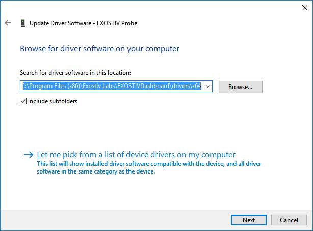
50 Select Browse my computer for driver software and specify the right location of the driver. - For 32 bits windows, the default directory is C:\Program Files\Exostiv Labs\EXOSTIVDashboard\drivers\x86 - For 64 bits windows, the default directory is C:\Program Files (x86)\exostiv Labs\EXOSTIVDashboard\drivers\x64 Installing the EXOSTIV Dashboard button in Vivado (Applies to EXOSTIV for Xilinx only) EXOSTIV for Xilinx provides a netlist flow, that enables EXOSTIV IP insertion after synthesis. This flow requires linking EXOSTIV Dashboard to Vivado using a shortcut to a script in Vivado s toolbar. This shortcut is automatically added at the end of the EXOSTIV Dashboard software installation. In cases where the installation program fails to locate the Vivado installation properly, it is possible that no button gets inserted in the Vivado toolbar. Please check your Vivado toolbar. If the EXOSTIV icon is NOT visible, then you have to install it manually: To install the EXOSTIV Dashboard shortcut into Vivado, please use one of the following procedures: Procedure #1 Through EXOSTIV Dashboard menu (semi-automatic). 1. Close Vivado. 2. Start EXOSTIV Dashboard 3. Click on the following menu item: Tools > Install Dashboard Shortcut Rev February 26,


51 4. You should receive the message: Integration with Vivado succeeded. Procedure #2 Setting it up from Vivado 1. Start Vivado 2. Click on the following meny item: Tools > Customize Commands > Customize commands 3. Hit on the green + button on the upper left corner: 4. Type EXOSTIV Dashboard in the dialog that opens. Press ENTER. Rev February 26,
52 5. Enter the following lines in the main dialog window: - Run command: source "C:/Program Files (x86)/exostiv Labs/EXOSTIVDashboard/vivado_server.tcl" -notrace - Select Add to the toolbar - Optionally add the following tooltip: Start EXOSTIV Dashboard - Icon file path: C:/Program Files (x86)/exostiv Labs/EXOSTIVDashboard/Exostiv-icon_32x32.png Please replace C:/Program Files (x86)/exostiv Labs/EXOSTIVDashboard with the alternate path that you used for installing the EXOSTIV Dashboard software. Rev February 26,


53 Installing EXOSTIV Dashboard Linux 1. Please refer to: - EXOSTIV Dashboard for Xilinx Technical specifications - EXOSTIV Dashboard for Intel Technical specifications to check the supported Linux distributions and versions. 2. Download the latest version of EXOSTIV Dashboard: go to: Pick the desired version and register to request the download. 3. Make the installer executable In the window manager, right-click on the installer. Select the Permissions tab and enable the Allow executing file as program checkbox. 4. Run the installer Double click on the installer to start the software installation. Click three times on Forward, then on Finish. Rev February 26,


54 At the end of the installation, two new icons appear on the desktop to start and uninstall the application. Rev February 26,


55 Before running the application EXOSTIV Dashboard requires libusb to access the probe. Type following command to install libusb: - sudo apt-get install libusb Enter the administrator password to complete the installation. Libusb requires administrator privilege to use the USB bus. To remove this limitation, proceed as follows: - Open file /lib/udev/rules.d/50-udev-default.rules in a test editor like gedit with administrator rights. - Search for the following line in the file: SUBSYSTEM=="usb", ENV{DEVTYPE}=="usb_device", MODE="0664" - Replace with this line: SUBSYSTEM=="usb", ENV{DEVTYPE}=="usb_device", MODE="0666" - Save the file. Integration with Vivado Linking EXOSTIV Dashboard to Vivado for Core Insertion requires using a shortcut to a script in Vivado s toolbar. In Vivado, open the Customize Commands dialog with Tools > Customize Commands > Customize Commands Click on the sign and enter EXOSTIV Dashboard as menu name and press Enter. Complete the fields on the right side as follows: Rev February 26,

56 Run command : source "/home/<user>/<exostiv installation directory>/vivado_server.tcl" -notrace Icon file path : /home/<user>/<exostiv installation directory>/exostiv-icon.png Replace <user> with the user name. Or adapt the path according to the installation folder. Click on OK to validate the changes and close the dialog box. The newly created custom command should now appear in the menu. A new button will appear in the toolbar. The new menu entry and the new button can now be used to start EXOSTIV Dashboard. Using the application from a command prompt The EXOSTIV Dashboard can be started from a command prompt. First go the install folder, typically cd./exostiv and execute command./exostivdashboard.sh. 6. Enter the following lines in the main dialog window: - Run command: source "C:/Program Files (x86)/exostiv Labs/EXOSTIVDashboard/vivado_server.tcl" -notrace - Select Add to the toolbar - Optionally add the following tooltip: Start EXOSTIV Dashboard - Icon file path: C:/Program Files (x86)/exostiv Labs/EXOSTIVDashboard/Exostiv-icon_32x32.png Please replace C:/Program Files (x86)/exostiv Labs/EXOSTIVDashboard with the alternate path that you used for installing the EXOSTIV Dashboard software. Rev February 26,
57 Appendix B Using Design Checkpoints (DCP) flow type (This section applies to EXOSTIV for Xilinx) Using Vivado with and without project files (.xpr) Xilinx Vivado provides several ways to define and implement FPGAs. The default usage of EXOSTIV implies defining projects files in Vivado (.xpr). However, in some cases, project files are not used especially when the target FPGA design is not synthesized with Vivado, but with a third-party EDA synthesis tool. A very common way of using Vivado is to proceed by successively saving Design Checkpoints (.DCP). Such checkpoints allow saving the state of the implemented design at any point of the flow. By using checkpoints, it is not mandatory to use project files (.xpr). The set of commands that can be used in Vivado differ on whether a project file is used or not. In this section, we present an alternate flow for using Vivado and EXOSTIV Dashboard without Vivado.xpr project file. Flow - We suppose that Vivado is used with the target FPGA design after synthesis. The synthesized design is loaded into Vivado as a netlist. Hence, the starting point is a design checkpoint (.DCP) saved with Vivado after loading the target FPGA design. We suppose that no Vivado project is defined. - In the EXOSTIV Dashboard, calling the implementation run is based on the preexistence of a Vivado project file. For this reason, the implementation of the FPGA design instrumented with the EXOSTIV IP cannot be started from EXOSTIV Dashboard. Hence, the option of starting the implementation from the EXOSTIV Dashboard must be de-selected. Rev February 26,
58 - After loading the synthesized design into Vivado (possibly recalling the corresponding design checkpoint), the EXOSTIV Dashboard can be linked to Vivado with the usual flow (please refer to section starting from Core Inserter - Overview ). Rev February 26,

59 - Pressing the Insert EXOSTIV IP button from the Insert EXOSTIV IP window of the Core Inserter will start and run the flow up the the Design Rules Check. Thereafter, the result is an instrumented synthesized design, that is, the same original design netlist, where a synthesized EXOSTIV IP is inserted and connected to the nodes chosen with the EXOSTIV Core Inserter. - Save your EXOSTIV Dashboard project file. - From there, the implementation of this instrumented design must be manually started. Here is how: 1. Switch to the Vivado session where the synthesized design had been loaded originally. The unit exi_top (EXOSTIV IP top) should be present in the design. Rev February 26,

60 2. Successively use the following commands from the Vivado command line interface: - Opt_design - (optionally: power_opt_design) - Place_design - (optionally: phys_opt_design) - Route_design - Write_bitstream <file name> Please refer to Vivado command line / batch mode user s guide for additional details and options. 3. You can then load the FPGA configuration and use EXOSTIV Analyzer. Rev February 26,
EXOSTIV Dashboard Hands-on - MICA board
 EXOSTIV Dashboard Hands-on - MICA board Rev. 1.0.5 - October 18, 2017 http://www.exostivlabs.com 1 Table of Contents EXOSTIV Dashboard Hands-on...3 Introduction...3 EXOSTIV for Xilinx FPGA Overview...3
EXOSTIV Dashboard. Tcl User's Reference Guide. Rev March 30,
 EXOSTIV Dashboard Tcl User's Reference Guide Rev. 1.0.0 - March 30, 2018 http://www.exostivlabs.com 1 Table of Contents Introduction...3 Short Help text...4 Long help text...10 Revision History Revision
Contents. Appendix B HDL Entry Tutorial 2 Page 1 of 14
 Appendix B HDL Entry Tutorial 2 Page 1 of 14 Contents Appendix B HDL Entry Tutorial 2...2 B.1 Getting Started...2 B.1.1 Preparing a Folder for the Project...2 B.1.2 Starting Quartus II...2 B.1.3 Creating
Tutorial for Altera DE1 and Quartus II
 Tutorial for Altera DE1 and Quartus II Qin-Zhong Ye December, 2013 This tutorial teaches you the basic steps to use Quartus II version 13.0 to program Altera s FPGA, Cyclone II EP2C20 on the Development
Vivado Design Suite User Guide
 Vivado Design Suite User Guide Design Flows Overview Notice of Disclaimer The information disclosed to you hereunder (the Materials ) is provided solely for the selection and use of Xilinx products. To
Employing Multi-FPGA Debug Techniques
 Employing Multi-FPGA Debug Techniques White Paper Traditional FPGA Debugging Methods Debugging in FPGAs has been difficult since day one. Unlike simulation where designers can see any signal at any time,
Vivado Design Suite User Guide
 Vivado Design Suite User Guide System-Level Design Entry Notice of Disclaimer The information disclosed to you hereunder (the Materials ) is provided solely for the selection and use of Xilinx products.
Chapter 2 Getting Hands on Altera Quartus II Software
 Chapter 2 Getting Hands on Altera Quartus II Software Contents 2.1 Installation of Software... 20 2.2 Setting Up of License... 21 2.3 Creation of First Embedded System Project... 22 2.4 Project Building
University of Massachusetts Amherst Computer Systems Lab 2 (ECE 354) Spring Lab 1: Using Nios 2 processor for code execution on FPGA
 Spring Lab 1: Using Nios 2 processor for code execution on FPGA") University of Massachusetts Amherst Computer Systems Lab 2 (ECE 354) Spring 2007 Lab 1: Using Nios 2 processor for code execution on FPGA Objectives: After the completion of this lab: 1. You will understand
University of Massachusetts Amherst Computer Systems Lab 2 (ECE 354) Spring 2007 Lab 1: Using Nios 2 processor for code execution on FPGA Objectives: After the completion of this lab: 1. You will understand
PlanAhead Release Notes
 PlanAhead Release Notes What s New in the 11.1 Release UG656(v 11.1.0) April 27, 2009 PlanAhead 11.1 Release Notes Page 1 Table of Contents What s New in the PlanAhead 11.1 Release... 4 Device Support...
Design Flow Tutorial
 Digital Design LU Design Flow Tutorial Jakob Lechner, Thomas Polzer {lechner, tpolzer}@ecs.tuwien.ac.at Department of Computer Engineering University of Technology Vienna Vienna, October 8, 2010 Contents
Vivado Design Suite User Guide
 Vivado Design Suite User Guide Design Flows Overview Notice of Disclaimer The information disclosed to you hereunder (the Materials ) is provided solely for the selection and use of Xilinx products. To
University of Massachusetts Amherst Computer Systems Lab 1 (ECE 354) LAB 1 Reference Manual
 LAB 1 Reference Manual") University of Massachusetts Amherst Computer Systems Lab 1 (ECE 354) LAB 1 Reference Manual Lab 1: Using NIOS II processor for code execution on FPGA Objectives: 1. Understand the typical design flow in
University of Massachusetts Amherst Computer Systems Lab 1 (ECE 354) LAB 1 Reference Manual Lab 1: Using NIOS II processor for code execution on FPGA Objectives: 1. Understand the typical design flow in
Quick Front-to-Back Overview Tutorial
 Quick Front-to-Back Overview Tutorial PlanAhead Design Tool This tutorial document was last validated using the following software version: ISE Design Suite 14.5 If using a later software version, there
Vivado Design Suite Tutorial. I/O and Clock Planning
 Vivado Design Suite Tutorial I/O and Clock Planning Notice of Disclaimer The information disclosed to you hereunder (the "Materials") is provided solely for the selection and use of Xilinx products. To
Building an Embedded Processor System on a Xilinx Zync FPGA (Profiling): A Tutorial
: A Tutorial") Building an Embedded Processor System on a Xilinx Zync FPGA (Profiling): A Tutorial Embedded Processor Hardware Design October 6 t h 2017. VIVADO TUTORIAL 1 Table of Contents Requirements... 3 Part 1:
Building an Embedded Processor System on a Xilinx Zync FPGA (Profiling): A Tutorial Embedded Processor Hardware Design October 6 t h 2017. VIVADO TUTORIAL 1 Table of Contents Requirements... 3 Part 1:
Adding the ILA Core to an Existing Design Lab
 Adding the ILA Core to an Existing Introduction This lab consists of adding a ChipScope Pro software ILA core with the Core Inserter tool and debugging a nonfunctioning design. The files for this lab are
Actel Libero TM Integrated Design Environment v2.3 Structural Schematic Flow Design Tutorial
 Actel Libero TM Integrated Design Environment v2.3 Structural Schematic Flow Design Tutorial 1 Table of Contents Design Flow in Libero TM IDE v2.3 Step 1 - Design Creation 3 Step 2 - Design Verification
Using Synplify Pro, ISE and ModelSim
 Using Synplify Pro, ISE and ModelSim VLSI Systems on Chip ET4 351 Rene van Leuken Huib Lincklaen Arriëns Rev. 1.2 The EDA programs that will be used are: For RTL synthesis: Synplicity Synplify Pro For
AN 839: Design Block Reuse Tutorial
 AN 839: Design Block Reuse Tutorial for Intel Arria 10 FPGA Development Board Updated for Intel Quartus Prime Design Suite: 17.1 Subscribe Send Feedback Latest document on the web: PDF HTML Contents Contents
I/O Planning Tutorial. PlanAhead Design Tool
 I/O Planning Tutorial PlanAhead Design Tool This tutorial document was last validated using the following software version: ISE Design Suite 15 If using a later software version, there may be minor differences
Vivado Design Suite Tutorial. I/O and Clock Planning
 Vivado Design Suite Tutorial I/O and Clock Planning Notice of Disclaimer The information disclosed to you hereunder (the "Materials") is provided solely for the selection and use of Xilinx products. To
Compiler User Guide. Intel Quartus Prime Pro Edition. Updated for Intel Quartus Prime Design Suite: Subscribe Send Feedback
 Compiler User Guide Intel Quartus Prime Pro Edition Updated for Intel Quartus Prime Design Suite: 18.0 Subscribe Send Feedback Latest document on the web: PDF HTML Contents Contents 1. Design Compilation...
ELEC 4200 Lab#0 Tutorial
 1 ELEC 4200 Lab#0 Tutorial Objectives(1) In this Lab exercise, we will design and implement a 2-to-1 multiplexer (MUX), using Xilinx Vivado tools to create a VHDL model of the design, verify the model,
Introduction. In this exercise you will:
 Introduction In a lot of digital designs (DAQ, Trigger,..) the FPGAs are used. The aim of this exercise is to show you a way to logic design in a FPGA. You will learn all the steps from the idea to the
PlanAhead Software Tutorial
 PlanAhead Software Tutorial I/O Pin Planning The information disclosed to you hereunder (the Information ) is provided AS-IS with no warranty of any kind, express or implied. Xilinx does not assume any
ISE Tutorial: Using Xilinx ChipScope Pro ILA Core with Project Navigator to Debug FPGA Applications
 ISE Tutorial: Using Xilinx ChipScope Pro ILA Core with Project Navigator to Debug FPGA Applications This tutorial document was last validated using the following software version: ISE Design Suite 14.5
Adding Custom IP to the System
 Lab Workbook Introduction This lab guides you through the process of creating and adding a custom peripheral to a processor system by using the Vivado IP Packager. You will create an AXI4Lite interface
Vivado Design Suite User Guide
 Vivado Design Suite User Guide Using the Vivado IDE Notice of Disclaimer The information disclosed to you hereunder (the Materials ) is provided solely for the selection and use of Xilinx products. To
16. Design Debugging Using In-System Sources and Probes
 June 2012 QII53021-12.0.0 16. Design Debugging Using In-System Sources and Probes QII53021-12.0.0 This chapter provides detailed instructions about how to use the In-System Sources and Probes Editor and
RTL Design and IP Generation Tutorial. PlanAhead Design Tool
 RTL Design and IP Generation Tutorial PlanAhead Design Tool Notice of Disclaimer The information disclosed to you hereunder (the "Materials") is provided solely for the selection and use of Xilinx products.
UNIVERSITY OF CALIFORNIA, DAVIS Department of Electrical and Computer Engineering. EEC180A DIGITAL SYSTEMS I Winter 2015
 UNIVERSITY OF CALIFORNIA, DAVIS Department of Electrical and Computer Engineering EEC180A DIGITAL SYSTEMS I Winter 2015 LAB 1: Introduction to Quartus II Schematic Capture and ModelSim Simulation This
University of Florida EEL 3701 Dr. Eric M. Schwartz Madison Emas, TA Department of Electrical & Computer Engineering Revision 1 5-Jun-17
 Page 1/14 Example Problem Given the logic equation Y = A*/B + /C, implement this equation using a two input AND gate, a two input OR gate and two inverters under the Quartus environment. Upon completion
LOG Storm Studio. User's Guide. Revision Jan Byte Paradigm
 1/24 Table of Contents 1Introduction... 4 2Starting up a... 4 2.1What do you need to get started?...4 2.2Connecting and configuring your LOG Storm device...4 3Using LOG Storm for the first time...6 3.1LOG
ISE Tutorial. Using Xilinx ChipScope Pro ILA Core with Project Navigator to Debug FPGA Applications. UG750 (v14.4) December 18, 2012
 December 18, 2012") ISE Tutorial Using Xilinx ChipScope Pro ILA Core with Project Navigator to Debug FPGA Applications UG750 (v14.4) December 18, 2012 Xilinx is disclosing this user guide, manual, release note, and/or specification
ISE Tutorial Using Xilinx ChipScope Pro ILA Core with Project Navigator to Debug FPGA Applications UG750 (v14.4) December 18, 2012 Xilinx is disclosing this user guide, manual, release note, and/or specification
Vivado Design Suite Tutorial. Design Flows Overview
 Vivado Design Suite Tutorial Design Flows Overview Notice of Disclaimer The information disclosed to you hereunder (the "Materials") is provided solely for the selection and use of Xilinx products. To
Using Xilinx ChipScope Pro ILA Core with Project Navigator to Debug FPGA Applications. UG750 (v12.3) November 5, 2010
 November 5, 2010") Using Xilinx ChipScope Pro ILA Core with Project Navigator to Debug FPGA Applications UG750 (v12.3) November 5, 2010 Xilinx is disclosing this user guide, manual, release note, and/or specification (the
Using Xilinx ChipScope Pro ILA Core with Project Navigator to Debug FPGA Applications UG750 (v12.3) November 5, 2010 Xilinx is disclosing this user guide, manual, release note, and/or specification (the
Cover TBD. intel Quartus prime Design software
 Cover TBD intel Quartus prime Design software Fastest Path to Your Design The Intel Quartus Prime software is revolutionary in performance and productivity for FPGA, CPLD, and SoC designs, providing a
Lab 3: Xilinx PicoBlaze Flow Lab Targeting Spartan-3E Starter Kit
 Lab 3: Xilinx PicoBlaze Flow Lab Targeting Spartan-3E Starter Kit Xilinx PicoBlaze Flow Demo Lab www.xilinx.com 1-1 Create a New Project Step 1 Create a new project targeting the Spartan-3E device that
Cover TBD. intel Quartus prime Design software
 Cover TBD intel Quartus prime Design software Fastest Path to Your Design The Intel Quartus Prime software is revolutionary in performance and productivity for FPGA, CPLD, and SoC designs, providing a
I/O Pin Planning Tutorial. PlanAhead Design Tool
 I/O Pin Planning Tutorial PlanAhead Design Tool Notice of Disclaimer The information disclosed to you hereunder (the "Materials") is provided solely for the selection and use of Xilinx products. To the
I/O Pin Planning Tutorial. PlanAhead Design Tool
 I/O Pin Planning Tutorial PlanAhead Design Tool Xilinx is disclosing this user guide, manual, release note, and/or specification (the Documentation ) to you solely for use in the development of designs
8PI Control Panel. User's Guide
 Revision.7 3 February 25 FCC Compliance This device complies with Part 5 of the FCC Rules. Operation is subject to the following conditions: () This device may not cause harmful interference, and (2) This
PlanAhead Software Tutorial
 PlanAhead Software Tutorial Team Design NOTICE OF DISCLAIMER: The information disclosed to you hereunder (the Information ) is provided AS-IS with no warranty of any kind, express or implied. Xilinx does
ISim In-Depth Tutorial. UG682 (v13.4) January 18, 2012
 January 18, 2012") ISim In-Depth Tutorial Xilinx is disclosing this user guide, manual, release note, and/or specification (the "Documentation") to you solely for use in the development of designs to operate with Xilinx
ISim In-Depth Tutorial Xilinx is disclosing this user guide, manual, release note, and/or specification (the "Documentation") to you solely for use in the development of designs to operate with Xilinx
PlanAhead Software Tutorial
 PlanAhead Software Tutorial RTL Design and IP Generation The information disclosed to you hereunder (the Information ) is provided AS-IS with no warranty of any kind, express or implied. Xilinx does not
TLL5000 Electronic System Design Base Module. Getting Started Guide, Ver 3.4
 TLL5000 Electronic System Design Base Module Getting Started Guide, Ver 3.4 COPYRIGHT NOTICE The Learning Labs, Inc. ( TLL ) All rights reserved, 2008 Reproduction in any form without permission is prohibited.
Best Practices for Incremental Compilation Partitions and Floorplan Assignments
 Best Practices for Incremental Compilation Partitions and Floorplan Assignments December 2007, ver. 1.0 Application Note 470 Introduction The Quartus II incremental compilation feature allows you to partition
Vivado Design Suite User Guide
 Vivado Design Suite User Guide Designing with IP UG896 (v2017.4) December 20, 2017 UG896 (v2017.3) October 04, 2017 Revision History The 12/20/2017: following Released table shows with Vivado the revision
ISE Simulator (ISim) In-Depth Tutorial. UG682 (v 13.1) March 1, 2011
 In-Depth Tutorial. UG682 (v 13.1) March 1, 2011") ISE Simulator (ISim) In-Depth Tutorial Xilinx is disclosing this user guide, manual, release note, and/or specification (the "Documentation") to you solely for use in the development of designs to operate
ISE Simulator (ISim) In-Depth Tutorial Xilinx is disclosing this user guide, manual, release note, and/or specification (the "Documentation") to you solely for use in the development of designs to operate
8. Best Practices for Incremental Compilation Partitions and Floorplan Assignments
 8. Best Practices for Incremental Compilation Partitions and Floorplan Assignments QII51017-9.0.0 Introduction The Quartus II incremental compilation feature allows you to partition a design, compile partitions
NIOS CPU Based Embedded Computer System on Programmable Chip
 1 Objectives NIOS CPU Based Embedded Computer System on Programmable Chip EE8205: Embedded Computer Systems This lab has been constructed to introduce the development of dedicated embedded system based
Tutorial StellarIP Interface To AXI Interface
 Tutorial StellarIP Interface To AXI Interface 4DSP LLC Email: support@4dsp.com This document is the property of 4DSP LLC and may not be copied nor communicated to a third party without the written permission
Using the ZC706 Zynq evaluation kit
 EXOSTIV Using the ZC706 Zynq evaluation kit Rev. 1.0.2 - November 6, 2017 http://www.exostivlabs.com 1 Table of Contents EXOSTIV using the ZC706 kit...3 Introduction...3 Using EXOSTIV with ZC706 evaluation
System Debugging Tools Overview
 9 QII53027 Subscribe About Altera System Debugging Tools The Altera system debugging tools help you verify your FPGA designs. As your product requirements continue to increase in complexity, the time you
Verilog Design Entry, Synthesis, and Behavioral Simulation
 ------------------------------------------------------------- PURPOSE - This lab will present a brief overview of a typical design flow and then will start to walk you through some typical tasks and familiarize
Vivado Design Suite Tutorial. Designing IP Subsystems Using IP Integrator
 Vivado Design Suite Tutorial Designing IP Subsystems Using IP Integrator Notice of Disclaimer The information disclosed to you hereunder (the "Materials") is provided solely for the selection and use of
AN 825: Partially Reconfiguring a Design on Intel Stratix 10 GX FPGA Development Board
 AN 825: Partially Reconfiguring a Design on Intel Stratix 10 GX FPGA Development Board Updated for Intel Quartus Prime Design Suite: 17.1 Subscribe Send Feedback Latest document on the web: PDF HTML Contents
Xilinx ChipScope ICON/VIO/ILA Tutorial
 Xilinx ChipScope ICON/VIO/ILA Tutorial The Xilinx ChipScope tools package has several modules that you can add to your Verilog design to capture input and output directly from the FPGA hardware. These
The Zynq Book Tutorials
 The Zynq Book Tutorials Louise H. Crockett Ross A. Elliot Martin A. Enderwitz Robert W. Stewart Department of Electronic and Electrical Engineering University of Strathclyde Glasgow, Scotland, UK v1.2
ADQ14 Development Kit
 ADQ14 Development Kit Documentation : P Devices PD : ecurity Class: : Release : P Devices Page 2(of 21) ecurity class Table of Contents 1 Tools...3 2 Overview...4 2.1 High-level block overview...4 3 How
TLL5000 Electronic System Design Base Module
 TLL5000 Electronic System Design Base Module The Learning Labs, Inc. Copyright 2007 Manual Revision 2007.12.28 1 Copyright 2007 The Learning Labs, Inc. Copyright Notice The Learning Labs, Inc. ( TLL )
ECE 3610 Microprocessing Systems Lab #1 Verilog Design of the TOC Using Quartus II
 ECE 3610 Microprocessing Systems Lab #1 Verilog Design of the TOC Using Quartus II This lab manual presents an introduction to the Quartus II Computer Aided Design (CAD) system. This manual gives step-by-step
Quick Tutorial for Quartus II & ModelSim Altera
 Quick Tutorial for Quartus II & ModelSim Altera By Ziqiang Patrick Huang Hudson 213c Ziqiang.huang@duke.edu Download & Installation For Windows or Linux users : Download Quartus II Web Edition v13.0 (ModelSim
Vivado Tutorial. Introduction. Objectives. Procedure
 Lab Workbook Introduction This tutorial guides you through the design flow using Xilinx Vivado software to create a simple digital circuit using VHDL. A typical design flow consists of creating model(s),
AN 825: Partially Reconfiguring a Design on Intel Stratix 10 GX FPGA Development Board
 AN 825: Partially Reconfiguring a Design on Intel Stratix 10 GX FPGA Updated for Intel Quartus Prime Design Suite: 18.1 Subscribe Latest document on the web: PDF HTML Contents Contents Partially Reconfiguring
ChipScope Inserter flow. To see the Chipscope added from XPS flow, please skip to page 21. For ChipScope within Planahead, please skip to page 23.
 In this demo, we will be using the Chipscope using three different flows to debug the programmable logic on Zynq. The Chipscope inserter will be set up to trigger on a bus transaction. This bus transaction
TP : System on Chip (SoC) 1
 1") TP : System on Chip (SoC) 1 Goals : -Discover the VIVADO environment and SDK tool from Xilinx -Programming of the Software part of a SoC -Control of hardware peripheral using software running on the ARM
TP : System on Chip (SoC) 1 Goals : -Discover the VIVADO environment and SDK tool from Xilinx -Programming of the Software part of a SoC -Control of hardware peripheral using software running on the ARM
EMT1250 LABORATORY EXPERIMENT. EXPERIMENT # 6: Quartus II Tutorial and Practice. Name: Date:
 EXPERIMENT # 6: Quartus II Tutorial and Practice Name: Date: Equipment/Parts Needed: Quartus II R Web Edition V9.1 SP2 software by Altera Corporation USB drive to save your files Objective: Learn how to
University of Florida EEL 3701 Dr. Eric M. Schwartz Department of Electrical & Computer Engineering Revision 0 12-Jun-16
 Page 1/14 Quartus Tutorial with Basic Graphical Gate Entry and Simulation Example Problem Given the logic equation Y = A*/B + /C, implement this equation using a two input AND gate, a two input OR gate
Vivado Tutorial. Introduction. Objectives. Procedure. Lab Workbook. Vivado Tutorial
 Lab Workbook Introduction This tutorial guides you through the design flow using Xilinx Vivado software to create a simple digital circuit using Verilog HDL. A typical design flow consists of creating
ISE Design Suite Software Manuals and Help
 ISE Design Suite Software Manuals and Help These documents support the Xilinx ISE Design Suite. Click a document title on the left to view a document, or click a design step in the following figure to
HyperBus Memory Controller (HBMC) Tutorial
 Tutorial") Synaptic Labs' HyperBus Memory Controller (HBMC) Tutorial T001: A Qsys based Nios II Reference design with HelloWorld test running in HyperRAM device using S/Labs' HBMC IP This tutorial describes a simple
Synaptic Labs' HyperBus Memory Controller (HBMC) Tutorial T001: A Qsys based Nios II Reference design with HelloWorld test running in HyperRAM device using S/Labs' HBMC IP This tutorial describes a simple
CPLD Experiment 4. XOR and XNOR Gates with Applications
 CPLD Experiment 4 XOR and XNOR Gates with Applications Based on Xilinx ISE Design Suit 10.1 Department of Electrical & Computer Engineering Florida International University Objectives Materials Examining
and 32 bit for 32 bit. If you don t pay attention to this, there will be unexpected behavior in the ISE software and thing may not work properly!
 This tutorial will show you how to: Part I: Set up a new project in ISE 14.7 Part II: Implement a function using Schematics Part III: Simulate the schematic circuit using ISim Part IV: Constraint, Synthesize,
ISim Hardware Co-Simulation Tutorial: Accelerating Floating Point FFT Simulation
 ISim Hardware Co-Simulation Tutorial: Accelerating Floating Point FFT Simulation UG817 (v 14.3) October 16, 2012 This tutorial document was last validated using the following software version: ISE Design
E85: Digital Design and Computer Engineering Lab 2: FPGA Tools and Combinatorial Logic Design
 E85: Digital Design and Computer Engineering Lab 2: FPGA Tools and Combinatorial Logic Design Objective The purpose of this lab is to learn to use Field Programmable Gate Array (FPGA) tools to simulate
Intel Quartus Prime Pro Edition User Guide
 Intel Quartus Prime Pro Edition User Guide Design Compilation Updated for Intel Quartus Prime Design Suite: 18.1 Subscribe Latest document on the web: PDF HTML Contents Contents 1. Design Compilation...
ChipScope Demo Instructions
 UNIVERSITY OF CALIFORNIA AT BERKELEY COLLEGE OF ENGINEERING DEPARTMENT OF ELECTRICAL ENGINEERING AND COMPUTER SCIENCE Overview ChipScope is an embedded, software based logic analyzer. By inserting an intergrated
Advanced module: Video en/decoder on Virtex 5
 Advanced module: Video en/decoder on Virtex 5 Content 1. Advanced module: Video en/decoder on Virtex 5... 2 1.1. Introduction to the lab environment... 3 1.1.1. Remote control... 4 1.2. Getting started
Vivado Walkthrough ECGR Fall 2015
 ECGR 2181 - Vivado Walkthrough 1 Vivado Walkthrough ECGR 2181 - Fall 2015 Intro In this walkthrough we re going to go through the process of creating a project, adding sources, writing vhdl, simulating
Introduction to Xilinx Vivado tools
 Introduction to Xilinx Vivado tools This document is meant to be a starting point for users who are new to using the Xilinx Vivado tools. The document will describe the basic steps to start, create, simulate,
VIVADO TUTORIAL- TIMING AND POWER ANALYSIS
 VIVADO TUTORIAL- TIMING AND POWER ANALYSIS IMPORTING THE PROJECT FROM ISE TO VIVADO Initially for migrating the same project which we did in ISE 14.7 to Vivado 2016.1 you will need to follow the steps
Xilinx Vivado/SDK Tutorial
 Xilinx Vivado/SDK Tutorial (Laboratory Session 1, EDAN15) Flavius.Gruian@cs.lth.se March 21, 2017 This tutorial shows you how to create and run a simple MicroBlaze-based system on a Digilent Nexys-4 prototyping
Vivado Design Suite Tutorial. Designing IP Subsystems Using IP Integrator
 Vivado Design Suite Tutorial Designing IP Subsystems Using IP Integrator Notice of Disclaimer The information disclosed to you hereunder (the "Materials") is provided solely for the selection and use of
Virtual Input/Output v3.0
 Virtual Input/Output v3.0 LogiCORE IP Product Guide Vivado Design Suite Table of Contents IP Facts Chapter 1: Overview Feature Summary..................................................................
AccelDSP tutorial 2 (Matlab.m to HDL for Xilinx) Ronak Gandhi Syracuse University Fall
 Ronak Gandhi Syracuse University Fall") AccelDSP tutorial 2 (Matlab.m to HDL for Xilinx) Ronak Gandhi Syracuse University Fall 2009-10 AccelDSP Getting Started Tutorial Introduction This tutorial exercise will guide you through the process of
AccelDSP tutorial 2 (Matlab.m to HDL for Xilinx) Ronak Gandhi Syracuse University Fall 2009-10 AccelDSP Getting Started Tutorial Introduction This tutorial exercise will guide you through the process of
Quartus II Version 14.0 Tutorial Created September 10, 2014; Last Updated January 9, 2017
 Quartus II Version 14.0 Tutorial Created September 10, 2014; Last Updated January 9, 2017 This tutorial will walk you through the process of developing circuit designs within Quartus II, simulating with
Quartus II Prime Foundation
 Quartus II Prime Foundation Course Description This course provides all theoretical and practical know-how to design programmable devices of ALTERA with Quartus Prime design software. The course combines
Design Verification Using the SignalTap II Embedded
 Design Verification Using the SignalTap II Embedded Logic Analyzer January 2003, ver. 1.0 Application Note 280 Introduction The SignalTap II embedded logic analyzer, available exclusively in the Altera
Name EGR 2131 Lab #6 Number Representation and Arithmetic Circuits
 Name EGR 2131 Lab #6 Number Representation and Arithmetic Circuits Equipment and Components Quartus software and Altera DE2-115 board PART 1: Number Representation in Microsoft Calculator. First, let s
User Guide. Introduction. Requirements. Installing and Configuring. C Interface for NI myrio
 User Guide C Interface for NI myrio Introduction The C interface for NI myrio is designed for users who want to program the NI myrio using the C programming language or a programming language other than
AN 797: Partially Reconfiguring a Design on Intel Arria 10 GX FPGA Development Board
 AN 797: Partially Reconfiguring a Design on Intel Arria 10 GX FPGA Updated for Intel Quartus Prime Design Suite: 18.1 Subscribe Latest document on the web: PDF HTML Contents Contents Partially Reconfiguring
Vivado Design Suite Tutorial. Using Constraints
 Vivado Design Suite Tutorial Using Constraints Notice of Disclaimer The information disclosed to you hereunder (the "Materials") is provided solely for the selection and use of Xilinx products. To the
Vivado Design Suite Tutorial: Programming and Debugging
 Vivado Design Suite Tutorial: Programming and Debugging Notice of Disclaimer The information disclosed to you hereunder (the "Materials") is provided solely for the selection and use of Xilinx products.
Altera Technical Training Quartus II Software Design
 Altera Technical Training Quartus II Software Design Exercises Quartus II Software Design Series: Foundation 2 Quartus II Software Design Series: Foundation Exercises Exercise 1 3 Exercises Quartus II
Vivado Design Suite Tutorial:
 Vivado Design Suite Tutorial: Programming and Debugging Notice of Disclaimer The information disclosed to you hereunder (the Materials ) is provided solely for the selection and use of Xilinx products.
Vivado Design Suite Tutorial. Designing with IP
 Vivado Design Suite Tutorial Designing with IP Notice of Disclaimer The information disclosed to you hereunder (the Materials ) is provided solely for the selection and use of Xilinx products. To the maximum
ISim Hardware Co-Simulation Tutorial: Accelerating Floating Point Fast Fourier Transform Simulation
 ISim Hardware Co-Simulation Tutorial: Accelerating Floating Point Fast Fourier Transform Simulation UG817 (v 13.2) July 28, 2011 Xilinx is disclosing this user guide, manual, release note, and/or specification
Creating a Processor System Lab
 Lab Workbook Introduction This lab introduces a design flow to generate a IP-XACT adapter from a design using Vivado HLS and using the generated IP-XACT adapter in a processor system using IP Integrator